Note: Descriptions are shown in the official language in which they were submitted.
CA 02681264 2009-09-18
WO 2008/116310
PCT/CA2008/000572
Method of Forming Waveguides Via Controlled Delamination and
Waveguides Formed Using the Method
TECHNICAL FIELD
[00011 This application relates to channel assemblies, including
waveguides, as well as
methods of forming waveguides and microchannel assemblies.
BACKGROUND
100021 Low-loss hollow waveguides with periodic claddings, in both fiber
and integrated
form, are emerging as an important class of optical devices. Potential
applications include
temperature-insensitive and tunable telecommunication devices, optical
analysis of small
volumes of gases or liquids, nonlinear optics in gases, novel slow light and
opto-mechanical
structures, and chip-scale optical interconnects. Integrated hollow waveguides
have
traditionally been fabricated by wafer bonding or by selective etching of a
sacrificial material.
SUMMARY
100031 A method of forming a waveguide is disclosed. A multilayer stack of
light guiding
layers is formed, and the multilayer stack is delaminated between at least two
of the light
guiding layers to form a waveguide between the light guiding layers.
[0004] A waveguide is also disclosed, comprising a multilayer stack of
light guiding
layers. The multilayer stack is delaminated in a patterned region between
light guiding layers.
100051 A waveguide is further disclosed, comprising a multilayer stack of
light guiding
layers. The multilayer stack has a patterned separation between at least a
first waveguiding
layer and a second waveguiding layer. The waveguide also comprises a
reflective overlayer
on the multilayer stack, and a reflective underlayer beneath the multilayer
stack.
[00061 A tapered waveguide is also disclosed, comprising a multilayer stack of
light
guiding layers. The multilayer stack has a patterned separation between at
least a first
waveguiding layer and a second waveguiding layer. The patterned separation has
converging
1
CA 02681264 2009-09-18
WO 2008/116310
PCT/CA2008/000572
sides in at least a first direction, and diminishing height in the first
direction.
[0007] A method of forming a channel is also disclosed. A metal layer is
deposited on a
substrate. An overlayer is deposited onto the substrate over the metal layer.
The metal layer is
induced to diffuse into the overlayer to form a region of reduced adhesion
between the
substrate and the overlayer. The overlayer is delaminated from the substrate
in the region of
reduced adhesion to form the channel between the overlayer and the substrate.
[0008] Another method of forming a channel is disclosed. A multilayer stack of
layers is
formed with at least two adjacent layers having a patterned region between
them.. The
adhesion between these adjacent layers is lower in the patterned region,
compared to the
adhesion between these same adjacent layers outside the patterned region. The
multilayer
stack is delaminated between these adjacent layers at the locations defined by
the patterned
region to form the channel embedded within the layers.
[0009] Here a new approach is described, wherein hollow microcharmels forming
a Bragg
waveguide assembly are fabricated by controlled formation of thin film
delamination buckles
within a multilayer stack. A hollow waveguide is formed by alternating layers
of the
multilayer stack forming light guiding surfaces. The hollow waveguide is
formed between
layers that delaminate from each other, as for example under applied stress to
one or more of
the layers. The multi-layer stack may be formed of alternating layers of low
and high index
of refraction materials, as for example forming omni-directional dielectric
reflectors. Metal
cladding of the waveguiding layers is also provided in one embodiment, as for
example by
providing a metal base layer and a cap layer. Methods of assembly are
disclosed, as well as
the assemblies themselves.
[0010] In any of the methods and apparatus' disclosed herein the waveguide may
be, for
example, a Bragg waveguide, or an anti-resonant reflection waveguide, and
furthermore may
be tapered along the direction of the waveguide axis.
2
CA 02681264 2009-09-18
WO 2008/116310
PCT/CA2008/000572
[0011] These and other aspects of the device and method are set out in the
claims, which
are incorporated here by reference.
BRIEF DESCRIPTION OF THE FIGURES
100121 Embodiments will now be described with reference to the figures, in
which like
reference characters denote like elements, by way of example, and in which:
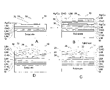
[0013] Figs. 1A-1D. The sequence of steps is shown for producing a buckled
hollow
waveguide with metal layers terminating the upper and lower cladding mirrors.
The end view
of a waveguide facet is shown in these illustrations. CHG is any chalcogenide
glass that
exhibits the Ag or Cu photodoping effect, LIM is a compatible low-index
material such as an
organic polymer, an Si02-based glass, or a hybrid of those, and M is a
reflective metal (or
combination of metals).
[0014] Figs 2A-2D. Schematic of a process used to form hollow waveguides by
buckling
delamination of a thin film mirror stack. The multilayer mirrors comprise high
and low index
silicon-based materials. LIM is the low index material, HIM is the high index
material, LAL
is a low adhesion layer, and M is a reflective metal or metals (optional). AP
is a change in
ambient pressure (such as occurs when removing a sample from the deposition
chamber) and
AT is a change in temperature (either incidental or applied). In some cases,
LIM and HIM
layers can be interchanged.
[00151 Figs. 3A-3D. Schematic of a process used to form hollow waveguides by
buckling
delamination of a single layer, followed by deposition of a multilayer. The
multilayer mirrors
are comprised of high and low index, silicon-based materials. LIM is the low
index material,
HIM is the high index material, LAL is a low adhesion layer, and M is a
reflective metal or
metals (optional). AP is a change in ambient pressure (such as occurs when
removing a
sample from the deposition chamber) and AT is a change in temperature (either
incidental or
applied).
[0016] Figs. 4A-4D. Schematic of a process used to form hollow waveguides by
buckling
delamination of a thin film mirror stack. The multilayer mirrors are comprised
of high and
3
CA 02681264 2009-09-18
WO 2008/116310
PCT/CA2008/000572
low index, silicon-based materials. LIM is the low index material, HIM is the
high index
material, LAL is a low adhesion layer, and M is a reflective metal or metals
(optional). SOL
is a compressively stressed overlayer, consisting of, for example, one or more
carbon or metal
sub-layers designed for high compressive stress and high reflectivity at the
wavelength of
interest.
[0017] Figs. 5A-5D. Schematic of an embodiment of a process used to form
hollow
waveguides. PAI is polyamide-imide and IG2 is Ge33As12Se55 glass. Fig. 5D:
evolution of the
compressive stress in a single IG2 layer on a silicon substrate versus the
number of Ag layers
(-25 rim thick) sequentially photodoped into the glass. The origin of the
horizontal axis
corresponds to the as-deposited film.
[0018] Figs. 6A-6E. Illustrations of images taken of a chip after the
buckling process. The
features illustrated are representative examples of the types of structures
that can be formed in
a single parallel process. (A) Illustration of a low magnification photograph
showing straight-
sided buckles. Although not visible in the illustration, the microchannels 22
may have
nominal widths from 10 to 80 gm (shown in groups of 5), and 80 to 20 pm and 80
to 10 gm
tapers. Sinusoidal s-bends 38, and rings 26 with diameters of 500 and 1000 gm
are illustrated.
In Fig. 6A, the distance between sets of 5 is roughly 1 cm. (B)-(E)
Illustration of optical
microscope photographs of various features: (B) 500 p.m diameter rings 26, (C)
20 and 40 pm
straight-sided guides, with buckled alignment mark features (crosses and
squares) in between,
(D) s-bends in 40 tun wide guides, and (E) sections of two adjacent tapers
(centre-to-centre
spacing 250 mm).
[0019] Figs. 7A and 7B. Illustrations of buckling delamination of a single
IG2 film. (a)
Buckling atop a 1 mm diameter Ag circle. Real-time evolution of the buckling
pattern occurs
as light induces photodoping of the underlying Ag into the IG2 film (and thus
loss of adhesion
of the IG2 film). Outside the Ag circle, the IG2 film remains well adhered to
the polymer
underlayer. (b) Buckling in a region where the Ag underlayer is continuous.
[0020] Figs. 8A and 8B. Analysis of the buckling process for the 4.5 period
upper mirror.
(a) Peak buckle height versus half-width (both in units of Am) according to
elastic buckling
4
CA 02681264 2014-09-08
theory (solid line). After photodoping and at ¨160 C, the bottom and
remaining IG2 layers
of the upper mirror were assumed to possess 200 and 100 MPa compressive
stress,
respectively (see Figs. 5D). Stress in the PAI layers was assumed negligible.
The markers
show some experimentally measured buckle heights for each of the nominal half-
widths
studied. (b) Illustration of a SEM image of a nominally 10 um wide buckle,
showing sharp
bending and some cracking near the buckle peripheries.
[00211 Figs. 9A and 9B. Illustrations of microscope photographs of straight-
sided buckles:
(a) 60 and (b) 80 p.m base width. The 60 um features show some localized,
small-scale
wrinkling along the axis of the channels. The wrinkling is more extensive and
significant for
the 80 gm features.
[00221 Figs. 10A-10D. Simulated reflectivity for various incidence angles
(from normal)
for (a) and (b) the bottom ODR (with IG2 and PAI layer thickness 145 nm and
290 nm,
respectively) and (c) and (d) the Ag-doped top ODR (with Ag:IG2 and PAI layer
thickness
150 and 290 nm, respectively, except for a 260 nm thick Ag:IG2 first layer).
The mirrors
were designed to provide overlapping omnidirectional stop bands near 1600 nm.
[00231 Figs. 11A-11F. Results from a commercial finite difference mode
solver. (a)-(e)
The intcnsity distributions for the 3 lowest order TE modal solutions at 1600
nm, respectively.
(d)-(e) The predicted radiation loss versus wavelength for the modes in parts
(a)-(c),
respectively. Results from a commercial finite difference mode solver, for a
waveguide with
40 gm base width and 2.5 um peak height
[00241 Fig. 12. Results for guidance of TE polarized light in buckled
waveguides with 40
um base width. Near field mode profiles: fundamental mode at 1610 nm, first
order mode at
1610 nm, and second order mode at 1586 nm were obtained. Fig. 12 shows a loss
estimate
from plot of scattered light versus distance along a straight, 40 um wide
waveguide. To
ensure a conservative estimate, data points associated with a scattering
defect near 2.4 mm
were removed. Scattered light (1595 nm wavelength) from a nominally 40 lIM
wide hollow
waveguide (¨ 5 mm in length) captured by an infrared camera were also
obtained. The
CA 02681264 2014-09-08
sinusoidal s-bend was 500 gm long with a 250 gm offset. Light was coupled at
left and the
output facet was visible at right.
[0025] Figs. 13A-13C. Wavelength dependence of TE polarized light guidance.
(a)
Simulated reflectivity of the lower ODR cladding, for TE polarized light at
normal (green)
and near-glancing (blue) incidence. (b) Simulated reflectivity of the upper
ODR cladding, for
normal incidence (green), and near-glancing incidence for TE (red) and TM
(blue) light. (c)
Measured transmission versus wavelength through a typical 40 gm wide hollow
waveguide,
mm in length.
[0026] Fig. 14. Reflectivity versus wavelength predicted for 4 period
IG2/PA1 mirrors,
without (dotted line) and with (solid line) a terminating Au layer. The first
(incident) IG2
layer was assumed to be 260 nm thick, while the remaining 3 IG2 layers were
assumed to be
145 nm thick. All 4 PAI layers (including the one adjacent to the Au in the
metal-terminated
case) were assumed to be 290 nm thick. The Au layer was assumed 50 nm thick,
and both
mirrors were assumed to lie atop a semi-infinite substrate with refractive
index 1.5.
[0027] Figs. 15A-15B. Plots of 1-R for the mirrors from Fig. 14, without
(dotted line) and
with (solid line) terminating Au layer. (a) TM polarized light at 88 degrees
from normal
incidence, (b) TE polarized light at 72 degrees from normal incidence.
[0028] Figs. 16A-16D. The sequence of steps is shown for producing a
buckled hollow
waveguide with metal layers terminating the upper and lower cladding mirrors.
[0029] Figs. 17A-17B. Fundamental air-guided TE mode profiles for a
waveguide with 20
gm base width and 1.8 gm peak height, as simulated using finite difference
software, at a
wavelength of: (a) 1620 nm, showing some penetration of the mode into the
lower mirror. (b)
1770 nm.
[0030] Fig. 18. Propagation loss versus wavelength (predicted by a finite
difference
numerical solver) is plotted for the fundamental air-guided TE mode of a
hollow waveguide
with 20 gm base width and 1.8 gm peak height. Au-terminated mirrors with
lossless Ag:1G2
and PA1 layers were assumed.
6
CA 02681264 2009-09-18
WO 2008/116310
PCT/CA2008/000572
100311 Fig. 19. Propagation loss versus wavelength (predicted by a finite
difference
numerical solver) is plotted for the fundamental air-guided TE mode of a
hollow waveguide
with 40 gm base width and 2.5 gm peak height. A fixed extinction coefficient
of 10-5 was
assumed for all Ag:IG2 and PAI layers.
DETAILED DESCRIPTION
100321 Listing of Reference Signs
CHG ¨ chalcogenide glass
LIM ¨ relatively low refractive index material
HIM ¨ relatively high refractive index material
M ¨ metal
Ag/Cu ¨ Silver or Copper
LAL ¨ low adhesion layer
SOL ¨ stressed overlayer
Ag ¨ Silver
PAI ¨ polyamide-imide
IG2 ¨ Ge33As12Se55 chalcogenide glass
Si ¨ Silicon
Ag:IG2 ¨ Silver-doped IG2
Au ¨ Gold
¨ waveguide
12 ¨ waveguide axis
¨ waveguide gap
Substrate ¨ any suitable substrate, for example Si.
22 ¨ microchannels
24 ¨ cross
26 ¨ circle
28 ¨ multilayer stack
¨ light guiding layers
32 ¨ patterned region
7
CA 02681264 2009-09-18
WO 2008/116310
PCT/CA2008/000572
34 ¨ converging sides
36 ¨ region of reduced adhesion
37 ¨ first direction
38 ¨ sinusoidal s-bends
40 ¨ square
42 ¨ overlayer film
44 ¨ first ODR
46 ¨ second ODR
48 ¨ patterned Ag layer in Figs. 7A and 7B
50 ¨ edges of the buckle in Fig. 8B
52 ¨ flat bottomed mirror
54 ¨ upper mirror
56 ¨ sidewalls
58 ¨ low loss band
[0033] Immaterial modifications may be made to the embodiments described here
without
departing from what is covered by the claims.
[00341 Buckling delamination of thin films is a fairly well understood
phenomenon in
itself. Within the regime of elastic deformation, the buckled areas are
characterized by an
increase in bending strain energy but a decrease in compressive strain energy.
Buckling of a
film can occur spontaneously, provided: (i) the compressive energy exceeds the
bending
energy for a given buckled width, and (ii) the energy release rate (per unit
area under the
buckle) is higher than the adhesion energy per unit area between the film (or
stack of films)
and its substrate. Various patterns may be constructed. Since film
delamination causes
catastrophic failure of microelectronic circuits or of protective barrier
coatings, buckling has
traditionally been studied as a problem to be avoided.
[0035] Referring to Figs. 1A-1D, desired buckle morphology for microfluidic
channels
and hollow waveguides is a straight-sided blister, commonly known as the Euler
column.
8
CA 02681264 2009-09-18
WO 2008/116310
PCT/CA2008/000572
Within elastic limits, and for a given equi-biaxial, pre-buckle stress level,
the Euler column
arises for only a restricted range of buckle width. However, if compressive,
bending, or shear
stresses exceed the yield stresses of the films undergoing delamination,
plastic deformation
also plays a role in determining the buckle shape.
[00361 To control the location and shape of delamination buckles, two distinct
properties
may be engineered. First, a technique for creating regions of low and high
adhesion is
required. Second, some means is required for accurately controlling the stress
within the
layers to be buckled. One embodiment of the process is guided self-assembly of
straight-
sided, Euler-like buckles by delamination of a multilayer stack 28, as
illustrated in Figs. 1-5.
100371 A method of forming a waveguide 10, and waveguide 10 itself is
disclosed.
Referring to Fig. 6E, the waveguide 10 may be tapered along the axis 12 of the
waveguide.
Referring to Figs. 1A-1D, a multilayer stack 28 of light guiding layers 30 is
formed, and the
multilayer stack 28 is delaminated between at least two adjacent light guiding
layers 30 to
form a waveguide 10 between the light guiding layer 30. The waveguide formed
may be a
waveguide core embedded within the light guiding layers 30. Referring to Fig.
1D, the
waveguide 10 is represented by a gap 20. In some embodiments, gap 20 may be a
hollow
microchannel or waveguide core. In other embodiments, gap 20 may be filled
with various
types of material. In some embodiments, the multilayer stack 28 is delaminated
in a patterned
region or separation 32 between light guiding layer 30. Referring to Fig. 1C,
delamination of
the multilayer stack 28 may occur along patterned region 32 between light
guiding layer 30.
Referring to Fig. 6E, the patterned region 32 may have converging sides 34,
and thus in some
embodiments, the waveguide 10 is tapered in both width and height along the
waveguide axis.
Referring to Fig. 2B, in some embodiments, the patterned region 32 is defined
by a region of
reduced adhesion 36 between light guiding layer 30. The region of reduced
adhesion 36 may
be characterized by a low-adhesion layer (LAL).
100381 Referring to Fig. 1C, in other embodiments, the multilayer stack 28 may
have a
patterned separation or delamination between at least a first waveguiding
layer and a second
waveguiding layer. In the embodiment illustrated in Fig. 1C, the first and
second waveguiding
9
CA 02681264 2009-09-18
WO 2008/116310
PCT/CA2008/000572
layers include the LIM and CHG layers that define gap 20. Each or both of the
first and
second waveguiding layers may consist of multiple individual layers. The
multilayer stack 28
may be delaminated at the patterned separation. Referring to Fig. 6E, the
patterned separation
may have converging sides 34 in at least a first direction 37, and diminishing
height in the
first direction.
[0039] Referring to Fig. 5B, the patterned region 32 may correspond to a
region of metal
to be subsequently doped into one or more of the light guiding layer 30s. In
the embodiment
of Fig. 5B, the metal to be subsequently doped into the light guiding layer 30
is illustrated as
Ag. Referring to Fig. 4B, the patterned region 32 may also correspond to a
region of surface
coating on one or more of the light guiding layer 30. The surface coating may
comprise, for
example, one or more of the materials listed in Table 3. In the embodiment of
Fig. 4B, the
surface coating is illustrated by the LAL layer.
[0040] The assembly technique is generally applicable to any material system,
and may
involve:
100411 Referring to Fig. 1A, a thermodynamically compatible pair of materials,
one with
relatively low refractive index (LIM) and the other with relatively high
refractive index
(HIM). Ideally, the refractive index contrast between the materials should be
sufficiently high
as to enable an omnidirectional dielectric reflector (ODR).
10042] An ability to tailor the compressive stress of either one or both of
the materials
above, and/or to augment their stress through the addition of a compressively
stressed
overlayer. By varying the deposition parameters, the magnitude of compressive
stress for
many standard thin film dielectrics can be controlled with high accuracy.
Referring to Fig.
4C, many metal and carbon-based films exhibit extremely high compressive
stress using
standard deposition techniques, and can be used as stressed overlayers (SOL).
[0043] Some means to create localized (patterned) regions 32 of reduced
adhesion at one
interface within the multilayer. Various techniques may be used for modifying
the adhesion
CA 02681264 2009-09-18
WO 2008/116310
PCT/CA2008/000572
energy of various materials, especially those used in silicon-based micro-
electromechanical
(MEMs) systems.
[0044] Self-assembled hollow Bragg waveguides may be made using standard
silicon
materials (Si, Si02, SiN,,, and/or amorphous metal-oxides), which find uses in
electronics and
MEMs industries. In the embodiments illustrated in Figs. 1-4, the reference
sign "substrate" is
used to illustrate the substrate used. It should be understood that the
substrate may be, for
example, any of the above-listed silicon materials, or any other suitable
substrate. The
materials are suited for controlling the stress of thin films, such as by
varying deposition
parameters, and for modifying the adhesion of such materials. Therefore, all
of the
requirements listed above can be met.
[0045] Referring to Figs. 3A-3D, a waveguide 10 is illustrated, comprising
light guiding
layer 30. In some embodiments, the light guiding layer 30 may comprise
alternating layers of
different index of refraction. The alternating layers may comprise a first
material having a
relatively low index of refraction and a second material having a relatively
high index of
refraction. The first material may comprise, for example, silicon dioxide or
an organic
polymer. Referring to Figs. 5A-5C, an example of the first material is
illustrated as
polyamide-imide (PAI). In addition, the second material may comprise, for
example, one or
more of chalcogenide glass CHG, amorphous silicon, polycrystalline silicon,
silicon nitride
and an amorphous metal oxide. Referring to Figs. 1A-1D, chalcogenide glass
(CHG) is
illustrated. In some embodiments, light guiding layer 30 may form omni-
directional dielectric
reflectors. Referring to Fig. 3D, in other embodiments, the multilayer stack
28 further
comprises at least one of a reflective overlayer and a reflective underlayer.
Referring to Fig.
3D, in some embodiments a reflective metal layer (illustrated in Fig. 3D by
the reference
numeral M)is applied to at least one of below and above multilayer stack 28,
or to both below
and above multilayer stack 28. In further embodiments, the multilayer stack 28
comprises
both a reflective overlayer and a reflective underlayer. The reflective
overlayer may be on the
multilayer stack 28, while the reflective underlayer may be beneath the
multilayer stack 28, as
illustrated in Fig. 3D by the reference numeral M. The overlayer and/or the
underlayer may
each comprise, for example, one or more metal films, such as, for further
example, nickel,
11
CA 02681264 2009-09-18
WO 2008/116310
1'CT/CA2008/000572
stainless steel or tungsten. The films may be reflective metal films. In some
embodiments, gap
20 may be formed by inserting a shaped sacrificial layer in the patterned
separation 32 during
formation of the multilayer stack 28. Subsequent removal of the sacrificial
material may then
complete the formation of gap 20. Embodiments such as these may be carried
out, for
example, in cases where a metal overlayer and a metal underlayer are present.
[0046] Si02 (with for example n-1.45-1.5) may, for example, be used, as the
LIM layer,
particularly in applications using air incidence due to a near optimal
refractive index in such
applications. For the high index layers, amorphous silicon, polycrystalline
silicon, silicon
nitride, or one of various amorphous metal-oxides, including Ta205, Ti02,
Hf02, Nb205,
Y203, and Zr02 may be used. Thus, numerous silicon-based material combinations
are
available for fabrication of Bragg filters and ODRs, satisfying the first
requirement.
[00471 The stress of a thin film material used in one of the layers can be
tuned over a wide
range (from compressive to tensile) by varying one or more deposition
parameters, or in some
cases by appropriate post-deposition annealing. This knowledge enables Bragg
mirrors and
ODRs to be deposited with accurately controlled stress distribution,
satisfying the second
requirement for the guided self-assembly of hollow waveguides 10 by buckling
delamination.
[00481 Referring to Fig. 4B, waveguide 10 may have, for example, a thin film
between the
multilayer stack 28 and the reflective overlayer. In the embodiment
illustrated in Fig. 4B, the
thin film is represented by the LAL layer. Referring to Fig. 3D, the overlayer
and/or the
underlayer may comprise a noble metal layer, illustrated for example as M.
[0049 Table 1 below shows representative stress tunability for various Si,
nitride, and
oxide-based films reported in the literature. As is standard, compressive
stress is assigned a
negative value and tensile stress a positive value.
Variables use
Thin film Deposition Stress range
to control
material technique [MPa]
stress
12
CA 02681264 2009-09-18
WO 2008/116310
PCT/CA2008/000572
PECVD (150 Film -370 to ¨
a-Si:H
C) thickness 130
Temp., gas -600 to
SiNõ PECVD
flow +500
-600 to
SiNõ PECVD Temp. =
+300
-270 to ¨
Si02 sputtering pressure
150
Substrate
TiO2 Ion beam -242 to ¨37
temp.
-900 to ¨
TiO2 sputtering pressure
250
-1000 to +
Nb205 sputtering Bias voltage
100
-470 to ¨
Nb205 Ion beam Bias voltage
370
-560 to ¨
Ta205 Ion beam Bias voltage
380
-150 to
Zr02 e-beam evap. Temp./ rate
+200
[0050] The intrinsic
stress of Si02 films (deposited by sputtering or physical vapor
deposition, etc.) is almost invariably compressive, and many high index
materials such as
those described above tend also to exhibit compressive stress. Furthermore,
the compressive
13
CA 02681264 2009-09-18
WO 2008/116310
PCT/CA2008/000572
stress of most of these materials can be tuned by controlling one or more
deposition
parameters (substrate temperature, chamber pressure, etc.), as summarized in
Table 1. This
list is representative, but far from exhaustive. The stress of most films,
regardless of
deposition technique, can be varied through control of the deposition
parameters. Other film
properties, such as optical loss and refractive index, also tend to vary with
deposition
parameters.
[0051] Many films exhibit extremely high intrinsic compressive stress,
including diamond-
like carbon (DLC) and metals such as nickel (Ni), stainless steel (SS), and
tungsten (W).
Such films may be used as highly stressed overlayers to induce buckling
delamination of an
underlying film.
[0052] Hybrid metal-dielectric mirrors can be used to produce very low loss
hollow
integrated waveguides 10. This has created the possibility of exploiting both
the high
reflectivity (to reduce radiation loss) and the compressive stress (to assist
in buckle formation)
of a suitable metal (or metals in a bilayer structure, etc.). Some metal films
that exhibit high
compressive stress (under appropriate conditions of deposition) are listed in
Table 2.
[0053] Table 2. Some compressively stressed metal films that might be used as
stressed
overlayers (SOL) in the buckling delamination of hybrid metal-dielectric
mirrors.
Deposition Compressive
Material underlayer
technique stress [GPa]
Nickel polycarbonate sputtering 1.5
Stainless
polycarbonate sputtering 1-2
steel
tungsten Si02/Si sputtering 2-2.5
[0054] Adhesion is one of the tribological properties of a film material
(the others are
friction and wear). Various methods for reducing the adhesion of Si, Si02, and
SiN), surfaces,
14
CA 02681264 2009-09-18
WO 2008/116310
PCT/CA2008/000572
may be used as for example by addition of an ultrathin coating film
(illustrated for example in
Fig. 4B as the LAL surface) or by chemical modification of the material
surface (the
distinction is somewhat arbitrary, based mainly on the technique used to
deposit the surface
layer). In some embodiments, the region of reduced adhesion may be created by
applying a
surface coating to one or more of the light guiding layer 30. As previously
mentioned, an
example of a surface coating is illustrated by the LAL layer in Fig. 4C. The
surface coating
may comprise, for example, one or more of the materials listed in Table 3. For
example, hard
inorganic films may be used as low adhesion surfaces, including diamond-like
carbon (DLC),
titanium nitride, titanium carbide, and silicon carbide. Also, many
hydrocarbon and
fluorocarbon films (such as Teflon) exhibit low adhesion and may also be used.
Organic self-
assembled monolayers (SAMs) may also be used as a means for chemically
modifying the
adhesion of silicon-based films. Some surfaces of interest and corresponding
low adhesion
layer (LAL) surface coatings are summarized in Table 3.
100551 If these
LALs are to be used, a few practical requirements must be satisfied. First,
if the LAL is to remain on the inner surface of the hollow waveguide 10 (ie.
as a surface layer
on the upper or lower cladding mirror), it ideally should be optically
transparent in the
wavelength range of interest, have low roughness, and have thickness much less
than the
wavelength of interest. Most of the LALs listed in Table 3 should meet these
requirements.
The LAL should also survive subsequent deposition of the upper Bragg
mirror/ODR. Many
of the LAL fihns/SAMs in Table 3 can survive to high temperature. This enables
the
processing temperature to be varied in accordance with optimizing the stress,
mechanical
properties, and optical properties of the upper mirror.
100561 Referring to Fig. 4B, in one embodiment of the method, the region of
reduced
adhesion may be created by modifying the adhesion energy of one or more of the
light
guiding layers 30, as illustrated by the LAL layer. Referring to Figs. 5B-5C,
in addition, the
region of reduced adhesion may be created by induced diffusion of an embedded
metal layer
(illustrated as Ag) into one or more of the light guiding layer 30.
CA 02681264 2009-09-18
WO 2008/116310
PCT/CA2008/000572
[0057] Table 3. Some low adhesion layers (LALs) for standard silicon-based
materials.
Layer thicknesses are typical, but are not necessarily limited to the value
shown.
LAL LAL
Material Low adhesion layer
deposition thickness
(surface) (LAL)
technique [nil)]
Dip-
silicon Perfluoropolyether < 10
coating
polysilicon fluoroalkysilane CVD ¨ 1
Various organic Vapor
Silicon ¨ 2
SAMs phase
Dip-
Si02 Dodecyltrichlorosilane 1.5
coating
Vapor
silicon Organosilane (SAMs) ¨ 1
phase
Pulsed < 100
silicon TiC
laser dep. nm
Plasma
silicon DLC > 25 nm
CVD
silicon SiC LPCVD ¨ 1000
[0058] Referring to Figs. 1B-1C, delaminating the multilayer stack 28 may
comprise
applying a stress to one or more of the light guiding layer 30. The stress may
be be applied by,
for example, a spontaneous release of pre-stressed light guiding layers. The
pre-stressed light
guiding layers may be intrinsically pre-stressed light guiding layers. In some
embodiments,
this stress may be intrinsic to the film deposition process, for example, and
may lead to
16
CA 02681264 2009-09-18
WO 2008/116310
PCT/CA2008/000572
spontaneous release of pre-stressed light guiding layer 30. In addition, the
stress to drive
delamination may be applied by heating of the multilayer stack 28, cooling of
the multilayer
stack 28, or changing pressure (illustrated in Figs. 2B-2C) applied to the
multilayer stack 28.
The stress may be compressive, for example. The stress may be applied by one
or more of the
above mentioned techniques.
[0059] Given the ability to control the stress and adhesion, various
process flows can be
used to fabricate hollow Bragg waveguides by buckling delamination of standard
silicon
electronics materials. Three alternative exemplary process flows (methods) are
described in
the following sub-sections.
[0060] Method 1 ¨ multilayer buckling driven by intrinsic stress of dielectric
layers
[0061] In the first method, the intrinsic compressive stress (arising from
film deposition) is
the main driver used to induce buckling delamination of a Bragg mirror or ODR.
Referring to
Fig. 2A, a low adhesion layer (LAL) is patterned using standard lithographic
techniques
(etching or liftoff) at a selected interface within the overall multilayer.
The process is
illustrated schematically in Figs. 2A-2D.
[0062] A detailed description of the process steps for method 1 is as
follows:
[0063] Referring to Fig. 2A, deposit a Bragg mirror or ODR onto a substrate
(illustrated as
substrate in Fig. 2A) of choice, to act as the lower cladding of the hollow
waveguides 10. The
stress of the layers in this lower mirror is relatively arbitrary (provided it
is not so high as to
cause mirror failure), so that the layer depositions should be optimized to
ensure maximum
reflectivity of the Bragg stack at the wavelength of interest. A highly
reflective metal layer
(or layers of metal, optimized for adhesion and reflectivity) may be deposited
prior to the
dielectric mirror, to reduce the radiation loss of waveguide modes. The metal
layer is
illustrated in Figs. 2A-2D as the layer M. The final (upper) dielectric layer
in this mirror can
be either the LIM or the HIM, depending on the layers chosen in the subsequent
steps.
[0064] Referring to Fig. 2A, deposit and pattern a low adhesion layer (LALs),
selected to
ensure preferential delamination between the upper and lower mirrors at the
locations of the
17
CA 02681264 2009-09-18
WO 2008/116310
PCT/CA2008/000572
LAL. While Fig. 2D shows the LAL remaining adhered to the bottom mirror after
buckling,
it might also be designed to adhere to the upper mirror.
[0065] Referring to Fig. 2B, deposit a Bragg mirror or ODR to act as the
upper cladding of
the hollow waveguides 10. The first (lowest) layer in this mirror can be
either the LIM or the
HIM, depending on the layers (LAL, etc.) chosen in the other steps. Within
this mirror, the
intrinsic stress is determined by the choice of deposition parameters. The
stress resultant for
the upper mirror is tuned to a suitable compressive value, such that straight-
sided
delamination buckles can form spontaneously (or after subsequent thermal
treatment or other
processing, as illustrated in Fig. 2C) over the patterned LAL strips from the
previous steps.
[0066] If buckles do not form spontaneously after the step in [0065], the
driving force for
delamination can be temporarily increased. For example, depending on the
thermal expansion
coefficients of the mirror materials relative to that of the substrate, either
cooling or heating
the sample will increase the compressive stress resultant in the upper mirror.
[0067] Referring to Fig. 2D, after buckling, a reflective metal overlayer
(illustrated as
layer M) can be deposited to reduce the radiation loss of modes guided in the
hollow core.
[0068] Method 2 ¨ buckling of a single layer followed by deposition of low-
stress layers
[0069] Referring to Figs. 3A-3C, another approach for fabricating a hollow
Bragg
waveguide 10 is to buckle a single, compressively stressed film lying atop a
patterned LAL.
Referring to Fig. 3D, this can be followed by the deposition of low-stress
HIM, LIM, and
metal layers to reduce the radiation loss of guided modes to the value
desired. An advantage
of this approach is that it can produce hollow cores of smaller dimensions,
since the
dimensions of straight-sided buckles scale with the thickness of the film (or
stack of films)
undergoing the buckling delamination. The process steps for Method 2 are shown
schematically in Figs. 3A-3D.
[0070] A detailed description of the processing steps for Method 2 is as
follows:
[0071] According to a method similar to that used in Method 1 as described
in paragraphs
[0063'40064].
18
CA 02681264 2009-09-18
WO 2008/116310
PCT/CA2008/000572
[0072] According to a method similar to that used in Method 1 beginning in
paragraph
[0060].
[0073] Referring to Fig. 3B, deposit a compressively stressed thin film,
either HIM or
LIM. This film acts as the first (lowest) layer in the upper cladding mirror
of the hollow
waveguides 10. Stress of this film is determined by the choice of deposition
parameters. It is
tuned to a suitable compressive value, such that straight-sided delatnination
buckles form
spontaneously (or after subsequent thermal treatment or other processing as
illustrated in Fig.
3C) over the patterned LAL strips from the previous steps.
[0074] If buckles do not form spontaneously after the step in [0073], the
driving force for
delamination can be temporarily increased. For example, depending on the
thermal expansion
coefficient of the compressively stressed layer described in [0073] relative
to that of the
substrate, either cooling or heating the sample will increase the compressive
stress of the layer
from the step in [0073].
[0075] Referring to Fig. 3D, after buckling, alternating LIM/HIM layers and
a reflective
metal overlayer M can be deposited to reduce the radiation loss of modes
guided in the hollow
core. The stress of these layers is tuned to a sufficiently low value that the
buckles formed in
previous steps remain stable.
[0076] Method 3 - multilayer buckling driven in part by a compressively
stressed
overlayer.
100771 Referring to Figs. 4C-4D, in this embodiment, delaminating the
multilayer stack 28
may comprise applying a compressively stressed overlayer (SOL) to the
multilayer stack 28.
The compressively stressed overlayer SOL may be, for example, a carbon-based
or metallic
layer. In addition, the compressively stressed overlayer SOL may comprise one
or more
carbon or metal films, such as, for example, nickel, stainless steel or
tungsten.
19
CA 02681264 2009-09-18
WO 2008/116310
PCT/CA2008/000572
[0078] Highly stressed overlayers can be used to drive the buckling
delamination of
underlying thin films. Thus, a third method for fabricating integrated hollow
Bragg
waveguides 10 is as shown in Figs. 4A-4D.
[0079] A detailed description of the processing steps for Method 3 is as
follows:
[0080] According to a method similar to that used in Method 1 as described in
paragraphs
[0063140064].
[0081] According to a method similar to that used in Method 1 beginning in
paragraph
[0060].
[0082] According to a method similar to that used in Method 2 beginning in
paragraph
[0070].
[0083] Referring to Fig. 4B, deposit a metallic overlayer film 42, to
increase the
compressive stress of the upper mirror and drive buckling delamination over
the LAL strips.
The metallic overlayer can consist of one or more metal sub-layers. Referring
to Fig. 4C, in
addition, adhering the compressively stressed overlayer SOL to the multilayer
stack 28 may
be accomplished with a thin film, for example, a thin layer such as Ti or Cr
(not shown) might
be used to ensure strong adhesion of the metallic overlayer to the upper
dielectric
mirror.Furthermore, this might be followed by a noble metal (not shown) with
high
reflectivity at the wavelength of interest (typically in the visible to near
infrared). Finally, as
illustrated in Figs. 4C-4D, a highly stressed metallic layer (illustrated as
the SOL layer) may
be added to cause the spontaneous formation of buckles over the LAL strips. In
some
embodiments, the compressively stressed overlayer is not metallic. After
delaminating the
multilayer stack 28 between light guiding layer 30, additional light guiding
layer 30 may be
deposited on the multilayer stack 28.
[0084] To illustrate the feasibility of our proposed methods, we consider a
specific
example based on the buckling of a 3 period Si/SiO2 multilayer with or without
a stressed
tungsten (referred to in this description as W) overlayer. If terminated by a
reflective metal
and designed for use in the 1550 nm wavelength region (where both Si and Si02
have good
CA 02681264 2009-09-18
WO 2008/116310
PCT/CA2008/000572
transparency), such a mirror has potential for reflectivity R>0.999. For the
analysis of
buckling, the mechanical properties of the thin film materials were assumed as
listed in Table
4.
[0085] Table 4. Mechanical properties used in the elastic buckling analysis
of a
multilayer.
layer Young's intrinsic
Poisson's stress
material thickness modulus
ratio
[nm] [GPa] [MPa]
polysilicon 110 150 0.22 -300
Si02 260 70 0.17 -200
varied 410 0.28 -2000
100861 Buckling of a multilayer stack 28 with or without a stressed overlayer
(as per the
schemes shown in Figs. 2A-2D and 4A-4D, respectively) may be analyzed using a
mathematical treatment that assumes a purely elastic buckling response. A plot
may be
derived of the energy release late (for propagation of a straight-sided Euler
buckle) and the
peak buckle height, both versus the buckle half-width (ie. the half-width of
the LAL strip
defined in Figs. 2A-2D and 4A-4D). For a straight-sided buckle formed by
spontaneous
delamination of a 3 period Si/Si02 multilayer, with a 200 nm thick W
overlayer, and for a
given set of intrinsic stresses, buckling is found to be only energetically
favorable above some
critical half width. Furthermore, for buckling to occur spontaneously the
energy release rate
must exceed the effective adhesion energy of the LAL interface. The addition
of the W
overlayer does not significantly affect the critical buckling half-width (it
is actually slightly
lower without the W layer), because the W layer adds both compressive stress
and significant
stiffness to the multilayer (W has a high elastic modulus). Rather, the main
role of the W
overlayer is to increase the driving force for delamination (ie. the energy
release rate), so that
buckling can occur spontaneously. This driving force increases with the W
layer thickness,
which can be adjusted once the effective adhesion energy of the LAL is known.
21
CA 02681264 2009-09-18
WO 2008/116310
PCT/CA2008/000572
[0087] Straight-
sided Euler buckles are predicted for delamination half-widths in the 20 to
50 tm range (approximately). Therefore, hollow waveguides 10 may be realized
based on the
buckling of a Si/Si02 multilayer. Due to the similar intrinsic stresses and
elastic moduli of all the
materials in Table 1, this conclusion can be extended to multilayers combining
any one of the
other high index materials with Si02.
[0088] Referring to Figs. 5A-5D and Figs. 6A-6F, in another embodiment,
microchannels
22 may be made within omnidirectional dielectric reflector (ODR) claddings
comprising thin
films of chalcogenide glass and polymer. Straight, curved, tapered and
crossing channels
22may be realized on a single wafer. The microchannels 22 may be formed by,
for example,
using the processes illustrated in Figs. 1-5, and Fig. 16. Referring to Fig.
6A, sinusoidal s-
bends 38 are illustrated, along with circles 26. As illustrated in Fig. 6C,
the patterned region
32 may be, for example, in the shape of cross 24, such that intersecting
waveguide
microchannels 22 are formed. Referring to Fig. 6C, the patterned region 32 may
also be in the
shape of a rectangle or square 40. Referring to Fig. 6B, the patterned region
32 may be, for
example, a circle 26, such that a dome or ring shaped waveguide microcharmel
22 is formed.
[0089] The region of reduced adhesion may be created by modifying the adhesion
energy
of one or more of the light guiding layer 30. Referring to Figs. 5B-5C, the
region of reduced
adhesion may also be created by induced diffusion of an embedded metal layer
(illustrated as
the Ag layer) into one or more of the light guiding layer 30. Control over
both adhesion
energy and compressive stress may for example be achieved through silver
photodoping of
chalcogenide glass layers. Photodoping is a well-known phenomenon, where
illumination of
a silver film in contact with a chalcogenide glass causes the silver to be
dissolved into the
glass. We can tune the compressive stress in a chalcogenide glass film by
photodoping
varying amounts of silver, as shown in the inset of Figs. 5A-5C. Under the
right conditions
(as described below), dissolution of an embedded Ag layer results in loss of
adhesion between
the adjacent chalcogenide film and an underlying polymer layer.
[0090] A
representative process flow (Figs. 5A-5C) is described briefly in the
following,
although various techniques of film deposition may be used. Referring to Fig.
5A, in one
22
CA 02681264 2009-09-18
WO 2008/116310
PCT/CA2008/000572
example, a series of alternating Ge33Asi2Se55 chalcogenide glass (illustrated
as IG2) (Vitron
AG) and polyamide-imide (PAI) polymer (Torlon AI-10, Solvay Advanced Polymers)
layers
(-150 nm and 290 nm thick, respectively) were deposited, starting and ending
with a polymer
layer, to form an 8.5 period first ODR 44. Referring to Fig. 5A, a thin silver
layer (-50 nm
thick) illustrated as Ag was patterned by liftoff on the top surface of this
mirror. Referring to
Fig. 5B, a second (4.5 period) ODR 46 was then deposited, starting with a
thicker (-260 nm)
IG2 glass layer (first layer only). In this ODR 46, a thin (-20 nm) silver
layer (Ag) was
deposited following each IG2 glass layer. Referring to Fig. 5C, aside from
tuning the stress,
dissolved Ag increases the thickness and refractive index of the IG2 layers,
thereby increasing
the peak reflectivity and omnidirectional bandwidth of the upper ODR, and
forming Ag:IG2
layers. Referring to Figs. 5B-5C, the PAI layers in the upper mirror were soft-
baked only (5
min at 90 C). As is typical for spun cast and cured polymer films, the PAI
layers are under
tensile stress at room temperature (in the 10-20 MPa range, as determined by
studying single
PAI layers). The tensile stress of these layers offsets the compressive stress
in the IG2 layers,
and inhibits the buckling of the stack 28 during its deposition.
100911 Following
deposition of the entire structure, the sample appeared essentially flat
and featureless. A two-step process may be used to initiate post-deposition
buckling as
described in the example following. Referring to Figs. 5B-5C, first, the
sample was exposed
to a high intensity (-0.1 W/cm2) white light source for approximately 1 day,
to drive
dissolution of Ag into the IG2 glass films to form the Ag:IG2 layers
illustrated in Fig. 5C.
Second, the sample was heated on a hot plate in a flowing nitrogen atmosphere.
Any
previously undissolved Ag diffuses into adjacent IG2 films during this baking
process,
increasing the stress of the IG2 layers in the upper mirror. In a typical
baking process,
empirically optimized by testing numerous samples, the temperature was ramped
at ¨5 C/min
up to 120 C, and then at ¨ 1 C/min until nearly all of the intended features
had buckled.
While we often observed some localized buckling after the white light
exposure, most of the
buckling features arise above some critical temperature (-160 C) during the
baking process.
As the temperature rises, the compressive stress of all layers increases (in
addition to the
stress increase caused by Ag dissolution) due to the higher thermal expansion
coefficients of
IG2 (-12x10-6K-1) and PAI (-30x10-6K-1) relative to the Si substrate (-3x10⁻⁶
K-1).
23
CA 02681264 2009-09-18
WO 2008/116310
PCT/CA2008/000572
Furthermore, the layers are more prone to deform plastically at elevated
temperature, as
discussed below. Referring to Fig. 5C, the end result is that the upper ODR 46
buckles in
locations defined by the patterned Ag layer, producing hollow channels
(similar to Euler
columns) surrounded by ODR mirrors (see Figs. 5 and 6). After buckling, the
sample was
slowly cooled to room temperature, and spun-cast with an overlayer of epoxy
(Norland
Optical Adhesive, NOA-73). Samples were cleaved after a brief immersion in
liquid
nitrogen, which improves the tendency of the PAI layers to fracture in a
brittle manner on
cleaving.
[0092] Dissolution of the Ag strips into the bottom IG2 layer of the upper
mirror is
believed to be akin to a 'disappearance' of the interfacial bonds in these
regions. Within the
upper mirror, delamination between the PAI and Ag-doped IG2 (Ag:IG2) layers is
avoided by
restricting the Ag thickness. Because of the order of deposition, sufficiently
thin Ag layers
are nearly completely dissolved into the IG2 layers during sputtering
deposition (due to the
kinetic energy of arriving Ag ions) or shortly afterward (due to routine light
exposure), and
subsequent PAI layers are found to adhere very well.
[0093] Some embodiments of this process enable the fabrication of a variety
of structures
on a single sample, as shown in Figs. 6A-6E. Referring to Fig. 6A, straight-
sided channels 22
of width 10 to 80 gm were realized in parallel, although the wider channels
(60 and 80 gm)
may exhibit some localized wrinkling along the channel (see Figs. 9A-9B),
likely due to the
onset of a secondary buckling mode. The ring structures 26 shown in Figs. 6
(a) and (b) are
somewhat unique, as they derive from embedded circles of Ag. These regions
delaminate
entirely during the baking step, forming a dome shape at high temperature. On
cooling to
room temperature, the centers of the domes collapse resulting in the self-
assembled, ring-
shaped channels shown. We have verified that these channels are hollow by
cleaving through
rings and inspecting their cross-section using an illustration of a SEM image.
The tapered
channels (Fig. 6 (e)) are tapered in both width and height, as per the
discussion below,
Referring to Fig. 6E, the tapered channels 22 have converging sides 34 in at
least the first
direction 37, and diminishing height in the first direction 34. Such
waveguides have been
studied theoretically in the context of slow light effects and out-of-plane
coupling.
24
CA 02681264 2009-09-18
WO 2008/116310
PCT/CA2008/000572
[0094] To theoretically analyze the buckling of the multilayers, we used
bulk material
properties for Ge33As12Se55 (IG2) glass and Torlon polyarnide-imide (PAI)
polymer. It should
be noted that the elastic modulus and other mechanical properties of a thin
film might be
different than the bulk counterparts. Furthermore, Ag doping of the IG2 glass
likely modifies
its mechanical properties.
[0095] The elastic modulus, Poisson's ratio, and coefficient of thermal
expansion (CTE)
of IO2 glass are approximately 21.9 GPa, 0.27, and 12x10-6 ICI, respectively.
The tensile and
flexural yield strengths of IG2 glass are on the order of 20-100 MPa. The
elastic modulus,
Poisson's ratio, and CTE of Torlon AI-10 (an unfilled grade of Torlon) are
approximately 3
GPa, 0.4, and 30x10.6 KA, respectively. Its tensile and flexural strengths are
on the order of
¨150 MPa at room temperature and ¨100 MPa at 150 C. Torlon PAI is amongst the
toughest
and strongest of all polymers, and exhibits exceptional retention of
mechanical properties over
a wide range of temperature (from cryogenic temperatures up to ¨250 C). This
poses a
challenge with respect to facet preparation, as mentioned above. When
extensively cured, the
PAI layers (such as in the lower mirror of the devices described) have a
tendency to stretch
and deform on cleaving (even after a bath in liquid nitrogen). Soft-baked
layers are less tough
and cleave more readily.
[0096] In early phases of the work, we studied the buckling delamination of
single layer
chalcogenide films. Figs. 7(a) and (b) show the delamination and buckling of a
single IG2
layer (-500 nm thick). The layer was deposited on top of a patterned Ag layer,
the position of
the Ag layer being indicated by reference sign 48 (-40 nm thick), which in
turn lies atop a
500 nm PAI layer on a silicon wafer. The Ge33Asi2Se55 layer was subsequently
deposited
with a second (non-patterned) Ag layer (also ¨40 nm thick) and then stored in
a refrigerator
for several months. The sample was removed from the refrigerator, allowed to
return to room
temperature, and then placed under the microscope. The microscope light-source
immediately induced photodoping of the Ag layers into the glass, causing loss
of adhesion at
the locations of the underlying Ag features. Fig. 7(a) shows a circular Ag
feature, over which
the IG2 film is partially delaminated. When the intensity of the microscope
light is increased,
Ag photodoping drives further delamination of the IG2 film and changes in the
buckle
CA 02681264 2009-09-18
WO 2008/116310
PCT/CA2008/000572
patterns. Note that the delamination does not extend outside the perimeter of
the underlying
Ag circle. We have observed (although did not record) straight-sided Euler
buckles forming
overtop straight-sided Ag strips on similar samples. Fig. 7(b) shows buckling
in a region
where the Ag underlayer 48 is continuous. Silver photodoping might be a
powerful technique
for studying the dynamic properties of thin film buckle formation.
[0097] The critical (minimum) compressive stress required to elastically
buckle a thin
isotropic plate or film (assuming sufficiently low adhesion in the latter
case) is given by the
well known expression:
2 E 111)2
12 1¨ v 2 (1)
[0098] where b is the half-width of the buckle, and h, E, and u are the
thickness, elastic
modulus, and Poisson's ratio of the plate or film, respectively. The Euler
column arises for
bo<b<2.5*bo (approximately), where bo is the minimum half-width for buckle
formation
given a pre-buckle stress level ao. Furthermore, the Euler buckle has a raised
cosine shape
with peak amplitude (ie. the height of the buckle at its centre) given by
(5õ,õõh 11-4(-2--cr ¨1) (2)
3 crc
[0099] Our buckling experiments on single IG2 films over pre-patterned Ag
strips
verified these relationships. For multilayers, buckling can be analyzed using
either an
effective medium approach or by considering each sub-layer individually. Based
on the latter
approach, and using the material parameters described above and layer
thicknesses described
below, predictions of the elastic buckling theory (for representative stress
levels, see Fig. 5D)
are plotted in Fig. 8(a) along with experimentally measured buckle heights.
[00100] The disagreement between the elastic theory and the experimental data
is larger
than can be explained by uncertainties in the moduli or compressive stresses
of the films.
Rather, it is likely due to the neglect of plastic deformation in the purely
elastic theory, as
follows. First, the stress levels employed are comparable to the yield
stresses of both the PAI
26
CA 02681264 2009-09-18
WO 2008/116310
PCT/CA2008/000572
polymer and the IG2 glass (see above), particularly at elevated temperature.
Second, the
aspect ratio (h/b, with h the total thickness of the upper ODR) for our
buckled structures is
outside the 'thin plate' limits specified for application of the elastic
theory. It is known that
buckling of 'thick' plates is accompanied by plastic deformation, and that the
corresponding
critical buckling stress is well below that predicted by the purely elastic
theory. The shape of
the smallest buckled features (see Fig. 8 (b)) supports this conclusion. The
profile is not well
described by a raised cosine function, and there is sharp bending (and even
evidence of
cracking in some cases) near the edges 50 of the buckle. Plastic deformation
is somewhat
beneficial in the present context, as it enables straight-sided buckles with
aspect ratios that
could not be produced by elastic deformation alone.
[001011 As
mentioned above, for elastic budding of a thin film (or stack of films), there
is
a restricted range of delamination widths that produce a straight-sided Euler
buckle. This is
because the initial buckling releases compressive strain in the direction
normal to the buckle
axis only. For sufficiently wide Euler columns, residual compressive strain
along the axis
causes secondary wrinkling in that direction. Even though the buckling
deviates from a
purely elastic process in the present case, we observed evidence for a
similarly restricted
range of straight-sided buckle widths. Figs. 6B-6e show 10, 20, and 40 gm wide
buckles,
which were consistently straight-sided for the process described. Figs. 9A-9B
shows typical
sets of 60 pm and 80 pm wide buckles (illustrated as microchannels 22) from
the same
process. These may exhibit regions of secondary wrinkling, and the wrinkling
is most
significant for the widest channels. This is likely the reason that the 40 pm
wide waveguides
exhibited the lowest loss (see below), in spite of the fact that the wider
waveguides have
larger (especially taller) hollow cores. For a given material system and layer
design, there
may be a restricted range of straight-sided buckle widths. Furthermore, this
range can be
controlled through appropriate design of the layers and their compressive
stress.
[001021 Waveguides 10 with Bragg reflector claddings (Bragg waveguides) were
originally proposed 30 years ago, and have received renewed interest due to
the recent
discovery of ODRs. Cladding a Bragg waveguide with an omnidirectional
dielectric reflector
27
CA 02681264 2009-09-18
WO 2008/116310
PCT/CA2008/000572
enables higher confinement of light to a hollow core, improved robustness
against defect
induced scattering, better fabrication tolerance, and potential for low-loss
waveguide bends
[00103] For Bragg waveguides with small (wavelength scale) core dimensions,
low
propagation loss is dependent on highly reflective cladding mirrors. Guidance
of linearly
polarized light is particularly challenging, due to the lower reflectivity of
a Bragg mirror for
TM polarized light (especially at high angles of incidence). A reduction in
the polarization
dependence of mirror reflectivity can be achieved by tuning the thickness of
the layer nearest
the air core. Referring to Figs. 11A-11C, for in-plane polarized light
guidance in the buckle
waveguides, the flat bottom mirror (illustrated generally as reference sign
52) effectively sees
TE polarized light. The upper (buckled) mirror (illustrated generally as
reference sign 54)is
curved, making it necessary to consider both polarization states. To reduce
radiation loss at
the `sidewalls' 56, the first layer of the upper mirror 54 was designed to be
approximately a
half wavelength thick.
[00104] Given the self-assembled shape of the hollow waveguides, an
accurate theoretical
analysis requires a numerical solution (see below). However, because the
waveguides of
interest have a low height to width ratio, a simplified slab model can be
expected to provide
some insight. Figs. 10A-B and 10C-D show the predicted reflectivity for the
upper and lower
cladding mirrors 54 and 52, respectively (in a planar model for the mirrors)
at various angles
of incidence and for both TE and TM polarization. The layer thicknesses were
estimated
from SEM images, and Ag photodoping was assumed to increase the refractive
index of the
IG2 layers in the upper mirror by 0.35.
[00105] Using a ray-optics model for a slab Bragg waveguide, the loss due
to sub-unity
mirror reflectivity is
a =10log10(Rm), (3)
[00106] where a is the loss in dB/cm, R is the mirror reflectivity (assumed
equal for both
mirrors) at the ray's angle of incidence, and M is the number of reflections
per centimeter of
waveguide length. For the fundamental mode and a core size considerably larger
than the
28
CA 02681264 2009-09-18
WO 2008/116310
PCT/CA2008/000572
wavelength of light, and neglecting penetration of light into the cladding
mirrors (which is
reasonable for high index contrast mirrors), it follows that
a ^--= ¨5A,logic, (R) (4)
D2
1001071 where X is the free-space wavelength in cm, and D is the thickness of
the hollow
core (ie. the mirror separation) in cm.
[00108I For the waveguides described here, the upper and lower cladding
mirrors are not
identical. Using the same approximations as above, the loss due to sub-unity
mirror
reflectivity is then
2.5A,
a ==-% __________________ D2 log10 (RR) (5)
[00109] where Rî and RB are the reflectivities of the top and bottom mirrors,
respectively.
[00110] The 40 gm wide waveguides described below have a peak core height of
¨2.5 gm.
Using this as the core thickness in the slab model, the incident angle for the
fundamental
mode ray is ¨72 degrees from normal at a wavelength of 1600 nm. From the data
in Figs.
10A-D, the relevant reflectivities for TE polarized light are RB-0.999 and Ri-
0.996. Using
these numbers in (5) produces a-14 dB/cm. Note that this estimate is
approximately valid for
all of the low-loss TE modes discussed below, since they are single-moded in
the vertical
direction.
1001111 Referring to Fig. 5C, the buckled waveguides 10 have a laterally
tapered shape
along the direction perpendicular to the waveguide axis 12 (shown in Fig. 6E),
which results
in an index guiding mechanism in that direction, that is, perpendicular to the
direction 37
(shown in Fig. 6E),. Furthermore, the effective width of the waveguides in the
lateral
direction (while difficult to define exactly) is relatively large and the use
of a Ä/2 first layer in
the upper mirror results in a reasonably high reflectivity (-0.98) for TM
light at near-glancing
incidence. The net result is that the radiation of TM polarized light through
`sidewalls' of the
waveguide is of secondary importance. This is evinced by assuming a lateral
effective core
29
CA 02681264 2009-09-18
WO 2008/116310
PCT/CA2008/000572
width of ¨10 gm (a somewhat arbitrary but conservative value) and an effective
mirror
reflectivity of 0.98 in the expressions above.
[001121 Since the slab model is only a rough approximation of the actual
structures (with
curved upper mirrors), a more accurate numerical solution was obtained using
commercial
finite difference software (Mode Solutions 2.0, Lumerical Solutions Inc.).
Referring to Figs.
11A-11C, for modeling purposes, we assumed the buckles to have a raised cosine
shape.
From profilometer measurements, this was verified to be a good assumption for
the wider (>
20 gm wide) buckles. Perfectly matched layer boundary conditions were used,
and the
simulation grid size was varied until further reduction produced no
significant changes in the
modal solutions. We used the same refractive index dispersion expressions and
layer
thicknesses as above, and neglected material absorption. Figs. 11A-F shows the
3 lowest-
order TE mode solutions at 1600 nm wavelength for a waveguide 10 with base
width 40 gm
and peak height 2.5 gm, along with their predicted loss (due to radiation
through the mirrors)
versus wavelength. Referring to Figs. 11A-11C, the three lowest order modes
are illustrated
as TEO, TE1, and TE2, respectively.
1001131 The low-loss bands in Figs. 11D-F correlate well with the
overlapping
omnidirectional stop bands shown in Figs. 10(a)-(d). From the ray optics
viewpoint, it is
expected that the low loss propagation band should be determined mainly by the
overlap of
the TE stop bands (of the lower and upper mirror) at ¨72 degrees incidence.
The low-loss
propagation band is also expected to correspond approximately to the
omnidirectional stop
band of the upper mirror, since guided light is effectively incident on the
upper mirror with a
range of angles and for both polarization states. Both interpretations are
consistent with the
numerical and experimental results. The numerical solution predicted ¨ 7 air-
guided TE
modes; the lowest order (lowest loss) modes are summarized in Table 5. Note
that the losses
of the TE modes are in reasonable agreement with the predictions of the ray
optics model as
expected. However, the low-loss bandwidth reduces slightly with increasing
mode order.
Predicted losses for TM polarized modes are much higher, consistent with our
experimental
observations.
CA 02681264 2014-09-08
[00114] Table 5. Low-order air-guided modes for a 40 um wide buckled
waveguide 10
with raised cosine profile and peak height 2.5 um, as predicted by a finite
difference inode
solver at 1600 nm wavelength.
mode effective index loss [dB/cm]
TE0 (100 % TE) 0.965 8.7
TEI (100 % TE) 0.958 11.7
TE2 (100 % TE) 0.950 15.1
TE1 (100 % TE) 0.942 18.7
IMO (100 % TM) 0.917 440
1001151 Light propagation was studied experimentally using both a tunable
laser and a
broadband light source. Source light was passed through fiber-based
polarization control
optics and then coupled into the hollow waveguides 10 using an objective lens.
A second
objective lens was used to collect light at the output facet. Output light was
delivered to one
of a photodetector, an infrared camera, or an optical spectrum analyzer, in
the latter case via
an iris, a fiber collimating optic, and a short length of standard single mode
fiber. To obtain
experimental mode field profiles, the magnified near-field images were focused
onto an
InGaAs CCD camera. The system was calibrated by imaging light from optical
fibers with
known mode-field diameters. For loss measurements, a multimode fiber (attached
to a
micropositioner) was used to scan the surface of a chip under test.
[00116] Guiding was verified for buckle base widths in the 20 to 80 pm
range. For the
reasons discussed above, we focus on results for waveguides 10 with 40 um base
width and
for in-plane (TE) polarized light. Experimental near field mode profiles at
the output facet of
an approximately 5 mm long waveguide 10 were produced for the first three
modes TEO,
TE I , and TE2. Consistent with the prediction of several low-loss TE modes,
we observed
multimode interference effects. By adjusting the input coupling position and
laser
wavelength, it was possible to excite different mode patterns at the output.
The 3 lowest-
31
CA 02681264 2014-09-08
order mode patterns (TEO, TE I, and TE2) are in good qualitative agreement
with the results
from the finite difference mode solver, and evidence of higher order modes was
also
observed. An exact quantitative comparison between experiment and theory was
limited by
the resolving power of the optics and by nonlinearities in the infrared
camera.
[001171 Propagation loss estimated from scattered light was as low as ¨1.5
dB/mm (see
Fig. 12). This is in reasonable agreement with the theoretical predictions
above, suggesting
that the loss is mainly determined by the reflectivity of the cladding
mirrors. Light guiding
through s-bends 38 was also observed.
[001181 In Figs. I 3(a) and (b), selected theoretical reflectivity curves
for the lower and
upper cladding mirrors 52 and 54, respectively, are repeated from Figs. 10A-B
and 10C-D.
Experimental verification (not shown) was obtained for thc bottom mirror,
revealing near-
perfect agreement above the electronic band edge of the materials. Fig. 13(c)
shows the
typical transmission versus wavelength through a hollow waveguide I 0, with
the wavelength
response of the test setup removed. A low-loss band 58 in the 1550 to 1700 nm
wavelength
range was found, with out of band rejection on the order of 40 dB. The
position and
bandwidth of the transmission passband are well correlated with the
omnidirectional
reflection bands of the cladding mirrors, in good agreement with the
predictions of the finite
difference simulation above. Note that the Ag-doped mirrors do not exhibit
high reflectivity
in the vicinity of the theoretically predicted (neglecting material loss)
third order stop band
near 700 nm. As a result, the waveguides 10 do not efficiently transmit light
in that range.
[001191 The loss of the waveguides 10 is comparable to that for other
integrated air-core
waveguides 10 (with similar core size) reported in the literature.
Nevertheless, it is always
desirable to reduce loss. This could be achieved by employing higher index
contrast mirror
materials (implying new process development) or by increasing the number of
periods in the
mirrors (implying increased process complexity and cost). However, it is known
that
reflectivity and bandwidth of finite period Bragg mirrors can be greatly
increased by adding
an 'outer' metallic layer. Preliminary analyses using the models described
above predict that,
32
CA 02681264 2009-09-18
WO 2008/116310
PCT/CA2008/000572
for core dimensions similar to those described here, loss below 1 dB/cm can be
achieved
using 4-5 period mirrors 'capped' by a thin (-50 nm) metal film.
[00120] Compared to conventional methods for fabricating hollow waveguides 10
and
microchannels, the approach described has potential advantages. The
delamination buckles
are driven by energy minimization, form spontaneously, and are quite stable.
We have
handled some samples extensively and verified their light guiding properties
over the course
of several months. Long and complex channel layouts (curved, crossing, and
tapered
channels, etc.) can be realized in a straightforward and parallel process.
While not yet
verified, it seems likely that the inner walls of buckled channels may exhibit
roughness
characterized by the film deposition process (which can be sub-nm), highly
advantageous for
low-loss light guiding and efficient fluid flow. The specific materials used
here provide
further advantages, including toughness, flexibility, resistance to cracking,
and a processing
temperature regime that is compatible with back-end integration on
electronics. However, the
approach described should be transferable to other material combinations,
provided means to
control compressive stress and interfacial adhesion are available.
[00121] The approach represents a new option for fabrication of hollow
channels and
waveguides 10 on planar platforms. The approach described should enable new
opportunities
for gas- and liquid-phase photonic integrated circuits.
[00122] In a further embodiment, adding thin gold layers to the cladding
mirrors can
reduce the propagation loss, increase the low-loss bandwidth, and simplify the
fabrication
process by reducing the overall number of films required. Simulations predict
loss on the
order of 1 dB/cm or less over ¨300 iun bandwidth, for cladding mirrors with as
few as 4-5
periods.
[00123] In a hollow Bragg waveguide 10, propagation loss is essentially
determined by the
reflectivity of the dielectric mirrors forming the claddings. In theory
(neglecting residual
absorption and scattering), propagation loss can be reduced to an arbitrarily
low value by
increasing the number of periods or the index contrast within the cladding
mirrors. However,
given the geometrical restrictions for realizing straight-sided buckles and in
the interest of
33
CA 02681264 2009-09-18
WO 2008/116310
PCT/CA2008/000572
fabrication simplicity, it is desirable to reduce the number of required
layers. Hybrid metal-
dielectric mirrors combine the best features associated with metallic mirrors
(ie. thinness) and
dielectric mirrors (ie. ultra-high reflectivity). Specifically, if a thin
metallic film is added as a
terminating layer, the stop band reflectivity and bandwidth of a few-period
dielectric stack
can approach the values associated with an infinite stack.
[00124] Using transfer matrix and finite difference simulations, we have
assessed the
potential benefits of using hybrid mirrors in our self-assembled waveguide
process. We
considered the role of both absorption and scattering losses in reducing
reflectivity.
According to the theoretical results, loss < 1 dB/cm is feasible for channels
with height ¨2 pm
using a slightly modified fabrication process. Specifically, the addition of
two thin metal
(Au) layers is predicted to enable a very significant reduction in loss (from
¨15 to ¨0.5
dB/cm), a significant increase in low-loss bandwidth (from ¨100 to ¨300 nm),
and a reduction
in the number of required film deposition steps (from ¨32 to ¨25).
[00125] To illustrate the enhanced performance of hybrid metal-dielectric
mirrors, we first
present results from a standard transfer matrix model. The planar mirrors
considered have
high and low index layers of Ge33As12Se55 (IG2) glass (photodoped by Ag) and
polyamide-
imide (PAI) polymer, respectively. Ag doping was assumed to increase the
refractive index
of the IG2 layers by 0.35, and for simplicity we initially neglected
absorption in both the glass
and polymer layers (this is discussed further below). The complex optical
constants of Au
were modeled using a closed-form expression. The simulated reflectivity for 4
period mirrors
with and without a terminating Au layer are compared in Fig. 14. The incident
IO2 layer of
the mirrors was set to be approximately twice as thick as the other IG2
layers, to improve the
stop band characteristics for TM light at incidence angles higher than the
Brewster angle of
the air-1G2 interface (-71 degrees). As discussed below, this comes at the
expense of
degraded stop band characteristics for TE polarized light, as well as for TM
polarized light
with incidence angles less than the Brewster angle.
[00126] As shown in Fig. 14, the non-metallized mirror exhibits far-from-
optimal stop
band characteristics. Especially for TM polarized light, the peak reflectivity
is much less than
1 for most incidence angles. In addition, the use of a double thickness first
IO2 layer
34
CA 02681264 2009-09-18
WO 2008/116310
PCT/CA2008/000572
produces a dip in reflectivity located near 1650 nm for normal incidence
light. For TE
polarized light, this reflectivity dip becomes narrower but deeper with
increasing incidence
angle (while shifting to shorter wavelength), and the effective bandwidth of
the stop band is
reduced relative to the case of a perfectly periodic mirror. The addition of
the terminating
metal layer dramatically improves the stop band features; the peak
reflectivity approaches 1
for both states of polarization, the intraband dip in reflectivity is nearly
eliminated, and the
stop band exhibits the square shape associated with a dielectric mirror of
large period count.
Selected data from Fig. 14 is re-plotted as (1-R) versus wavelength in Figs.
15A-B, so that
reflectivities approaching 1 can be compared on a log scale.
[00127] While metallic loss was taken into account, the preceding results were
obtained
under the assumption of ideal (transparent and flat) dielectric layers. For
the metal-capped
mirror, peak reflectivity >0.9999 is predicted. In practice, residual losses
within the dielectric
layers will reduce the peak reflectivity relative to the ideal value. These
residual losses arise
from absorption in the dielectric layers, scattering by rough interfaces, and
scattering due to
volume inhomogenieties. It should be stressed that fabrication of mirrors with
reflectivity on
the order of 0.9999 is not trivial. Following are analytical approximations
for the absorption
and scattering losses in a high reflectivity Bragg mirror:
KH + KL
VL rze 2,n0 2 2
nH - nL
(6)
SSL 87r2 T (n2 ¨ n2 ¨12
HL H L
[00128] where VL is the reflectivity reduction due to absorption and volume
scattering
within the dielectric layers and SSL is the reflectivity reduction due to
scattering induced by
surface roughness between layers. nH and riL are the refractive indices of the
high and low
index layers (-2.9 and ¨1.65 here), and no is the index of the incident
medium. ICH and KL are
the effective extinction coefficients of the high and low index layers, taking
into account both
volume absorption and scattering effects. THL is the Fresnel transmittance for
a single
interface between a high and low index layer, a is the RMS surface roughness
(assumed equal
for each interface), and is the free-space wavelength. For a mirror to have
R>0.9999, the
CA 02681264 2009-09-18
WO 2008/116310
PCT/CA2008/000572
sum of VL and SSL must be less than 1O'. Given the indices for the present
mirrors, and
assuming operation near 1550 nm wavelength, this means that the materials must
have low
effective extinction coefficients, (KH+KL)<104, and that the interfaces must
have low
roughness, cs<1 nm.
[00129] IG2 glass has very low intrinsic absorption (K102-1(ï7) in the 1500
mn wavelength
region. Ag photodoping of a chalcogenide glass shifts its band edge to longer
wavelengths,
but typically causes only a slight increase in absorption in the infrared
region. From
waveguide studies, it is possible to place an upper bound on the extinction
coefficient of PAI
in the 1550 nm wavelength range (Kpm<10-5). This is in agreement with loss
reported for
similar polymers in the 1-1.6 p.m wavelength range; a vibrational overtone of
the C-H bond
results in higher loss in the 1.6-1.8 gm range. We have previously reported
that the RMS
roughness of 1G2/PAI multilayers is as low as ¨0.2 nm. Based on these numbers,
it should be
feasible to achieve R>0.9999 for IG2/PAI mirrors operating at k< 1.6 gm.
[00130] Referring to Figs. 16A-16D, the hybrid metal-dielectric structures
proposed here
may be fabricated with only slight modifications to our established process as
described in
methods 1, 2, and 3 beginning on paragraphs [0060], [0070], and [0076],
respectively.
Referring to Fig. 16A, first, a metallized Si substrate is used as a base. The
only technological
issues for this layer are that the metal chosen must adhere well to the Si
substrate and that the
subsequent polymer layer must adhere well to the metal. The first issue is
easily addressed by
using standard metal bi-layers such as Ti-Au or Cr-Au. In the embodiment
illustrated in Figs.
16A-16D, Au is used. With respect to the second issue, one of the attributes
of the PAI
polymer used is its good adherence to many metals (including Au). Referring to
Fig. 16D, the
second modification to the process is that a thin Au layer is deposited as the
final step, thus
having no direct impact on the buckle formation. Since this layer can be very
thin, it is not
expected to modify the properties of the pre-existing buckles. The wafers can
then be coated
with a polymer over-layer to provide long-term protection against mechanical
or
environmental damage (not shown).
[00131] Consider hollow waveguides 10 of the type illustrated in Fig. 16D,
with a 4 period
upper mirror 54 and a 5.5 period lower mirror 52. The higher period count in
the bottom
36
CA 02681264 2009-09-18
WO 2008/116310
PCT/CA2008/000572
mirror compensates for the slightly reduced reflectivity associated with an
incident polymer
(ie. lower refractive index) layer, and results in nearly equivalent peak
reflectivity for the two
mirrors. As above, the PAI layers were assumed 290 nm thick, and the Ag:IG2
layers were
assumed 145 nm thick. An exception is the first Ag:IG2 layer (nearest the
hollow core) in the
upper ODR, which was set to a thickness of 260 nm to reduce polarization
dependent loss in
the waveguides 10. Ag doping was assumed to increase the refractive index of
each IG2 layer
(in both the upper and lower cladding mirrors) by 0.35. We consider two buckle
sizes, with
base widths of 20 and 40 gn. The low height to width aspect ratio of the
buckled hollow
channels enables reasonably accurate loss predictions using a ray-optics slab
model:
5A,
a log 0 (R)
(7)
[00132] where a is loss (due to leakage through the mirrors) in dB/cm, X.
is free-space
wavelength in cm, D is the core thickness in cm, and R is the effective
reflectivity of the
cladding mirrors at the ray's angle of incidence. We used transfer matrix
simulations to
estimate the appropriate mirror reflectivities; the losses predicted by
equation (7) are
summarized in Table 6.
[00133] Table 6. Estimated propagation loss at X=1600 nm, for self-
assembled hollow
waveguides with two different core sizes and metal-capped mirrors as described
in the main
text.
Approximate
Peak Estimated
Waveguide Ray Mirror
core propagation
base width incidence reflectivity,
height, loss
angle
D [pm] [dB/cm]
[degrees]
20 1.8 64 0.99991 -0.96
40 2.5 72 0.99993 - 0.39
37
CA 02681264 2009-09-18
WO 2008/116310
PCT/CA2008/000572
[00134] We reiterate that mirror reflectivity >0.9999 is feasible (at least
for )<1.6 gm) for
the PAI/IG2 material system, but would require a very tightly controlled
fabrication process
to ensure layer thickness uniformity and to minimize contaminants and
roughness.
[00135] Referring to Figs. 17A-17B, a more accurate analysis of the waveguides
10 was
conducted using a commercial finite difference mode solver (Mode Solutions
2.0, Lumerical
Solutions, Inc.). Waveguides 10 with both 20 and 40 gm base width were
simulated, using
the same layer thicknesses, number of mirror periods, and material parameters
described
above. Typical fundamental TE mode solutions are shown in Figs. 17A-B. The
mode is well
confined to the air core, except for some penetration into the first PAI layer
of the bottom
mirror (especially nearer the short wavelength side of the guiding pass band).
1001361 In initial simulations, the Ag:IG2 and PAI layers were assumed
lossless. A typical
plot of loss versus wavelength for a 20 gm waveguide 10 (peak channel height
1.8 m) is
shown in Fig. 18. The propagation loss in this case is due to absorption in
the outer metallic
layers (mostly) and radiation through the mirrors. The predicted propagation
loss is on the
order of 1 dB/cm (as low as ¨0.6 dB/cm) over a wavelength range spanning 300
nm. This
level of loss is in good agreement with the predictions of the ray optics
model.
[00137] Next, we considered the impact of lossy IG2 and PAI layers. For
simplicity, a
fixed extinction coefficient (kpAi=k1G2) was assumed across the entire
wavelength range
simulated. The loss of PAI (and other similar polymers) in the near to mid
infrared is mainly
attributable to molecular vibrational overtones, and is therefore very
wavelength dependent.
However, the extinction coefficient of PAI does not exceed ¨10-5 in the main
wavelength
range of interest here, and that of Ag:IG2 is expected to be even lower. Thus,
we use a fixed
extinction coefficient on this order as a worst case limiting value.
1001381 Fig. 19 shows a typical plot of loss versus wavelength for a waveguide
10 with 40
gm base width and 2.5 p.m peak channel height. In this case, a nominal Ag:IG2
layer
thickness of 130 mn was assumed and the first Ag:IG2 layer in the top cladding
was set to
240 nm thick. A fixed extinction coefficient (kpm=k1G2=1(T5) was assumed for
all of the
dielectric layers. For this level of material loss, the propagation loss of
the air-guided mode is
38
CA 02681264 2009-09-18
WO 2008/116310
PCT/CA2008/000572
predicted to be < 1 dB/cm over a 300 tun bandwidth. The minimum loss (-0.4
dB/cm) is
again in good agreement with the ray optics based prediction above. Note that
the
propagation loss increases slightly for shorter wavelengths within the pass
band, due to the
increased penetration of the mode into the bottom mirror discussed above.
1001391 Referring to Figs. 5A-5C, a method of forming a channel 22 is also
disclosed.
Referring to Fig. 5A, a metal layer is first deposited on a substrate. In the
embodiment
illustrated in Fig. 5A, the metal layer is illustrated as, for example an Ag
layer, and the
substrate is illustrated as, for example a PAI layer. The metal layer may
comprise a metal
film, and may be patterned on the substrate. In addition, as illustrated in
Fig. 5A, the substrate
may comprise at least one underlayer. Referring to Fig. 5B, an overlayer is
deposited onto the
substrate over the metal layer. In the embodiment of Fig. 58, the overlayer is
illustrated as,
for example, 1G2. The overlayer may be, for example, chalcogenide glass.
Referring to Fig.
SC, the metal layer is induced to diffuse into the overlayer to form a region
of reduced
adhesion 36 between the substrate and the overlayer. The overlayer is
delarninated from the
substrate in the region of reduced adhesion 36 to form the channel 22 between
the overlayer
and the substrate. The induced diffusion may be caused by the addition of at
least one of heat,
light, or a change in pressure. In some embodiments, the induced diffusion is
caused by the
addition of heat and light. Inducing the metal layer to diffuse increases the
compressive stress
of the overlayer, and causes the overlayer to delaminate from the subtstrate
in the region of
reduced adhesion. The channel 22 may comprises a waveguide channel as
illustrated.
1001401 Another method of forming a channel is disclosed. A multilayer stack
of layers is
formed with at least two adjacent layers having a patterned region between
them. The
adhesion of these adjacent layers is lower in the patterned region, compared
to the adhesion
between these same adjacent layers outside the patterned region. The
multilayer stack is
delaminated between these adjacent layers in the locations defined by the
patterned region to
form the channel embedded within the layers.
39
CA 02681264 2009-09-18
WO 2008/116310
PCT/CA2008/000572
[00141] Patterned region in this document may refer to, for example, a
patterned region,
patterned separation, or patterned delamination.
[001421 In the claims, the word "comprising" is used in its inclusive sense
and does not
exclude other elements being present. The indefinite article "a" before a
claim feature does
not exclude more than one of the feature being present. Each one of the
individual features
described here may be used in one or more embodiments and is not, by virtue
only of being
described here, to be construed as essential to all embodiments as defined by
the claims.