Note: Descriptions are shown in the official language in which they were submitted.
CA 02681958 2009-09-25
WO 2008/118440 PCT/US2008/003916
MEASURING AIR QUALITY USING A
MICRO-OPTICAL MECHANICAL GAS SENSOR
BACKGROUND OF THE INVENTION
1. Field of the Invention
[00011 The present invention generally relates to measuring air quality
using a sensor, and, more particularly, to a system and method for measuring
air
quality using a micro-optical mechanical gas sensor.
2. Description of the Related Art
[0002] There is growing public awareness and concem about the adverse
effects of indoor air quality on human health and productivity in public
buildings, work places and personal dwellings. Media attention concerning
toxic mold and related health effects as well as the outbreak of infectious
diseases such as SARS has led to renewed attention to indoor air quality in
homes, commercial buildings, schools and hospitals. See Instrument Society of
America (ISA), "Air-Pollution Sensors Forecast 25% Growth by 2003",
InTech, September, 1999.
[0003] Current commercial air quality monitoring devices are large
expensive analytical instruments, such as mass spectrometers and
spectroscopes, that are often restricted to monitoring a small number of
atmospheric pollutants. Each type of device has its advantage and
disadvantages. For example, optical absorption spectroscopy devices are
sensitive and selective, but are expensive and non-robust. Electrochemical /
electroadsorptive devices, although inexpensive and portable, typically are
CA 02681958 2009-09-25
WO 2008/118440 PCT/US2008/003916
limited to sensing only one gas. Mass spectroscopy devices are sensitive, but
are expensive and requires vacuum technology. Finally, chromatography
devices are sensitive, but expensive, non-portable, and non-robust.
[0004] A variety of methods are available for simultaneously detecting a
number of components in a gas mixture. For example, Raman spectroscopy,
Fourier Transform Infrared ("FTIR") spectroscopy, and mass spectroscopy may
be used. While these methods have their merits, they also have their
drawbacks. Cumbersome vacuum technology, an essential part of mass
spectroscopy, limits its portability. FTIR spectroscopy typically employs
absorption spectroscopy, which, in order to achieve high sensitivity, requires
the use of some form of White cell, see White, J. U., J. Opt. Soc. Am. 32,285
(1942), where pathlengths of up to kilometers may be attained. See Hanst, P.
L., "Pollution: Trace Gas Analysis" in "Fourier Transform Infrared
Spectroscopy", etd. J. R. Ferraro & L. J. Basile, vol.2,79-110, Academic
Press,
Inc. (1979). The use of some form of White cell restricts ruggedness since
careful alignment of the infrared beam entering and leaving the cell is
required.
SUMMARY OF THE INVENTION
[0005] A system and method for measuring air quality using a micro-
optical mechanical gas sensor is disclosed. According to one embodiment of
the present invention, the system includes an emission source that includes a
conduit gap for receiving a gas; a plurality of electrodes for applying an
electric
field to at least a portion of the conduit gap, the application of the
electric field
creating a plasma in the conduit gap; and a detector that detects an emission
2
CA 02681958 2009-09-25
WO 2008/118440 PCT/US2008/003916
from the plasma. The emission source and the detector may be micro-optical
mechanical devices.
[0006] According to one embodiment, the width of the conduit gap is less
than 100 microns. In another embodiment, the width of the conduit gap is less
than 10 microns.
[0007] The detector may be an optical detector, a charge coupled device, a
photodiode, or a spectrometer. The emission source and the detector may be
located on the same chip.
[0008] In one embodiment, the emission source may also include partially
transmitting mirrors in the conduit gap. In another embodiment, the emission
source may include a spacer having a passage within the conduit gap.
[0009] The system may include a controller that controls the emission
source and the detector. The controller may receive and process signals from
the detector.
[0010] A method for measuring air quality is discloses. According to one
embodiment, the method includes the steps of (1) placing a chip containing an
emission source and a detector in a gas flow; (2) applying an electric field
to at
least a portion of a conduit gap within the emission source, the electric
field
creating a plasma; (3) detecting an emission from the plasma; and (4)
processing data related to the detected emission to determine at least one
constituent of the gas flow.
3
CA 02681958 2009-09-25
WO 2008/118440 PCT/US2008/003916
[0011] According to one embodiment, the width of the conduit gap is less
than 100 microns. In another embodiment, the width of the conduit gap is less
than 10 microns.
[0012] The emission source and the detector may be micro-optical
mechanical devices.
[0013] The step of detecting an emission from the plasma may include the
step of detecting the emission with at least one of an optical detector, a
charge
coupled device, a photodiode, and a spectrometer.
[0014) The method may also include the step of altering a strength of the
electric field based on the detected emission.
[0015] The method may further include the step of displaying an identity
of the at least one constituent.
[00161 According to another embodiment, a system for measuring air
quality is disclosed. The system includes a controller and a plurality of
micro-
optical mechanical sensor in communication with the controller. Each micro-
optical mechanical sensor may include an emission source having a conduit gap
for receiving a gas, a plurality of electrodes for applying an electric field
to at
least a portion of the conduit gap, the application of the electric field
creating a
plasma in the conduit gap, and a detector that detects an emission from the
plasma.
[00171 According to one embodiment, the width of the conduit gap is less
than 100 microns. In another embodiment, the width of the conduit gap is less
than 10 microns.
4
CA 02681958 2009-09-25
WO 2008/118440 PCT/US2008/003916
[0018] The detector may be an optical detector, a charge coupled device, a
photodiode, or a spectrometer. The emission source and the detector may be
located on the same chip.
[0019] It is a technical advantage that a system and method for measuring
air quality using micro-optical mechanical gas sensor are disclosed. It is
another technical advantage that the system may include an emission source and
a detector that may be micro-optical mechanical devices. It is another
technical
advantage that the emission source may include a conduit gap, and the width of
the conduit gap is less than 100 microns.
BRIEF DESCRIPTION OF THE DRAWINGS
[0020] For a more complete understanding of the present invention, the
objects and advantages thereof, reference is now made to the following
descriptions taken in connection with the accompanying drawings in which:
[0021] Fig. 1 is a block diagram of the system for measuring air quality
using micro-optical mechanical gas sensor according to one embodiment of the
present invention;
[0022] Fig. 2 is schematic of a microplasma conduit according to one
embodiment of the present invention;
[0023] Fig. 3 is a flowchart depicting a method for measuring air quality
using micro-optical mechanical gas sensor according to one embodiment of the
present invention;
CA 02681958 2009-09-25
WO 2008/118440 PCT/US2008/003916
[0024] Figs. 4a to 4e are schematics of a method for creating a micro-
optical mechanical gas sensor according to one embodiment of the present
invention;
[0025] Fig. 5 is a schematic of a microplasma conduit according to one
embodiment of the present invention;
[0026] Fig. 6 is a schematic of a spacer according to one embodiment of
the present invention.
DETAILED DESCRIPTION OF PREFERRED EMBODIMENTS
[0027] Preferred embodiments of the present invention and their
advantages may be understood by referring to Figs. 1-6, wherein like reference
numerals refer to like elements.
[0028] In order to employ the attractive features of compactness,
portability, sensitivity and robustness in a single, integrated platform, the
present invention includes a micro-optical mechanical ("MOMS")-based device
for real-time monitoring of a variety of chemical species in the atmosphere.
According to one embodiment of the present invention, the core of the device
is
a gas sensor that employs emission spectroscopy integrated with a direct
current
glow discharge as the emission source.
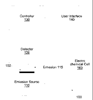
[0029] Referring to Fig. 1, a block diagram of a system for measuring air
quality using micro-optical mechanical gas sensor is provided. According to
one embodiment of the present invention, the system includes four general
components: emission source 110, detector 120, controller 130, and user
interface 140. In general, emission source 110 produces light emission 115
that
6
CA 02681958 2009-09-25
WO 2008/118440 PCT/US2008/003916
is detected by detector 120. Controller 130 controls both emission source 110
and detector 120, and communicates with user interface 140. Each element will
be described in greater detail below.
[0030] One or more of emission source 110, detector 120, controller 130,
and user interface 140 may be cofabricated or colocated. In another
embodiment, these elements may be fabricated and/or located separately.
[0031] Referring to Fig. 2, a simplified schematic of emission source 110
according to one embodiment of the present invention is provided. Emission
source 110 includes microplasma conduit, or conduit gap, 210 in which plasma
220 is developed. In one embodiment, microplasma conduit, 210 ranges in
width from sub-microns to tens of tens of microns In a preferred embodiment,
the width of microplasma conduit 210 is less than tens of microns.
[0032] Two ends of microplasma conduit 210 are open to allow a sample
of gas or entrained gaseous mixture to enter at one end and exit at the other.
An
example gas flow is indicated by arrows 230.
[0033] Emission source 110 further includes conducting electrodes 240
that are disposed on opposite sides of conduit gap 210. In one embodiment,
conducting electrodes 240 may be covered with a thin barrier layer (not
shown).
An example of a thin barrier layer would is barium titanate. Voltage source
250
applies to conducting electrodes 240 a voltage sufficient to produce an
electric
field. Examples of suitable voltage sources include Ultravolt model 1 AA24,
available from Ultravolt, Inc. Ronkonkoma, NY 11779. An example suitable
voltage range is between 0 and 1000 Volts. In one embodiment, a voltage
source with a variable output voltage, such as the Ultravolt 1 AA24, is useful
7
CA 02681958 2009-09-25
WO 2008/118440 PCT/US2008/003916
because the breakdown voltage required to create plasma depends on a number
of factors including sample gas composition, electrode material, electrode
configuration, etc. The electromagnetic field creates glow discharge 220.
[00341 In one embodiment, the electric field may be direct. In another
embodiment, the electric field may be alternating. In one embodiment, an
alternating electric field may be modulated. This may be performed in order to
reduce signal noise to detector 120.
[0035] The use of micro-systems technology to manufacture emission
source 110 of the present invention provides several advantages over
conventional devices. In one embodiment, emission source 110 and detector
120 may be delivered on a single, integrated platform. Due to this size,
system
100 may be provided in a handheld device.
[0036] In addition, because the emission source of the present invention
may be created using a process that is similar to integrated circuit
processing,
multiple sophisticated devices with demanding tolerances, and three
dimensional forms, may be made simultaneously. In one embodiment, this may
range to manufacturing thousands to millions of devices simultaneously. This
allow for efficient manufacture of the emission source. Moreover, mixed
functionality (electronics, sensing, optics, etc) may be realized on one
common
base, offering tiny systems with automatic self-referenced alignment, and
robustness.
[0037] In one embodiment, emission source 110 may be manufactured as
a replaceable cartridge.
8
CA 02681958 2009-09-25
WO 2008/118440 PCT/US2008/003916
[0038] On-chip optical detection permits a wide variety of gaseous species
to be measured quickly, accurately and cheaply because optical alignment
issues do not have as great of an impact as they would in a macrosystem. With
on-chip optical detection, the pathlength the emitted light has to travel from
the
emission source to the detector is small. For example, the pathlength may be
about 1 mm or less. This short pathlength permits all of the emitted light to
reach the detector, thereby providing a strong signal. In a macrosystem
counterpart, the pathlength may be from tens to hundreds of centimeters. Due
to this length, mirrors are typically used to reduce the footprint of the
pathlength. The inclusion of mirrors requires careful alignment to ensure that
all the light is directed to the detector. Such alignment is very susceptible
to
vibrations and mechanical shock, typically requiring a work surface that is
relatively immune from such interferences. Even so, regular checking of the
alignment is required for optimal operation.
[0039] According to one embodiment of the present invention, emission
source 110 may be operated as a series of optical resonant cavities, tuned for
a
particular constituent of the sample by a plurality of partially transmitting
mirrors 260, 265 disposed oppositely on opposing sides of conduit 210 and
perpendicular to the plane of conducting electrodes 240 and perpendicular to
the plane of gas flow 230. The optical resonant cavity causes light of a
particular wavelength, for example ki, to be reflected a large number of
times,
leading to an increase in the signal-to-noise ratio. This leads to an increase
in
sensitivity in the detection of the species of interest. The two partially
transmitting mirrors are separated by a distance 1, which defines the length
of
the optical cavity. The partially transmitting mirrors have a reflectivity
close to
9
CA 02681958 2009-09-25
WO 2008/118440 PCT/US2008/003916
one. In one embodiment, the reflectivity may be 0.995, meaning that 99.5% of
incident light striking the mirror is reflected. The number of modes of the
cavity is given by the relationship 1z n=ki/2.
[0040] In another embodiment, an additional sensor, such as
electrochemical cell 160, may be provided for calibration of detected light
emission. An output signal from the electrochemical cell 160 may serve as
secondary input to controller 130 to provide a reference signal for output
from
detector 120 for calibration.
[0041] In one embodiment, emission source 110 may act as a waveguide
for the light from the conduit. Referring to Fig. 6, in one embodiment,
emission source 110 may include spacer 610 that separates electrodes 240 from
at a fixed distance from each other. In one embodiment, spacer 610 may
include passage 620. In one embodiment, passage 630 may be in a center
portion of spacer 610. Passage 630 permits gas to flow in a direction that is
perpendicular to spacer 620 and parallel to electrodes 240.
[0042] In order for light to be transmitted from conduit 210 to detector
120, spacer 610 may be made of a material that is suitable for the
transmission
of electromagnetic energy in the wavelength range of interest. In one
embodiment, spacer 610 may be made of polymethyl methacrylate (PMMA).
In another embodiment, spacer 610 may be made of fused silica. Spacer 610
may not only function to separate electrodes 240, but to guide light from
conduit 210 to detector 120. Spacer 610 may render unnecessary additional
auxiliary items, such as an optical fiber, fiber bundle, etc.
CA 02681958 2009-09-25
WO 2008/118440 PCT/US2008/003916
[0043] Referring again to Fig. 1, in one embodiment, detector 120 is
placed directly above emission source 110 to collect the spectrum of light
emitted by plasma 220. In another embodiment, detector 120 may be located
remotely from emission source 110, and may use a fiber optic (not shown) or
fiber optic bundle (not shown) to deliver the emitted light from emission
source
110 to detector 120.
[0044] In one embodiment, optical window 150 may be provided and
located directly above the microplasma conduit. One suitable material for the
window is magnesium fluoride. In one embodiment, window 150 may have a
limited spectral range, for example, of 200 nm to 6 gm, with 80% or greater
transmission. Other window materials and properties thereof may be used as
necessary and/or desired.
[0045] Detector 120 is preferably an optical detector that is capable of
responding to a portion of the wavelength range of the emitted light. Detector
120 may be a single unit, or it may include multiple units operating in series
or
in parallel. Peaks and bands in the measured spectrum characteristic of the
emission spectra of a constituent, or more than one constituent, of the sample
are identified with the detector's associated electronics.
[0046] In one embodiment, detector 120 may include a charge coupled
device (CCD) and a monochromator. An example of a suitable CCD device is a
liquid nitrogen-cooled, silicon-array detector, such as the Spectrum One-F24
detector, available from Horiba Ltd. This CCD device has a 512 x 512 pixel
array and a spectral range of 300 nm to 1100 nm. An example of a suitable
monochromator is the TRIAX 320, also available from Horiba Ltd. This
11
CA 02681958 2009-09-25
WO 2008/118440 PCT/US2008/003916
monochromator has three different diffraction gratings: 1800 g/mm, 1200
g/mm and 300 g/mm. The resolution for the 1200 g/mm grating is 0.06 nm.
[0047] In another embodiment, detector 120 includes a photodiode or
photodiode array that may be provided with a filter. Example filters include a
narrow bandpass filter and a narrow bandpass filter wheel. A dispersion
element, such as a Rowand circle or diffraction grating, may also be provided.
[0048] In still another embodiment, detector 120 may be a spectrometer.
[0049] Controller 130 may be provided to control emission source 110,
detector 120, and user interface 140. In one embodiment, controller 130 may
be a microprocessor-based controller. Controller 130 may perform several
functions, including regulating power provided to emission source 110, and
controlling the operation of detector 120. Controller 130 may control multiple
emission sources 110, detectors 120, and/or user interfaces 140.
[0050] In one embodiment, controller 130 may process signals received
from detector 120 and provide output for user interface 140. In one
embodiment, the signal processing involves determining the relative
intensities
and wavelengths of the measured signals and, through comparison against a
library database or pre-set, known reference points, identification of
components in the gas sample. In an embodiment where a plurality of detectors
120 are networked, controller 130 may process signals for multiple detectors
120.
[0051] In another embodiment, controller 130 may store signals for later
retrieval by a separate device.
12
CA 02681958 2009-09-25
WO 2008/118440 PCT/US2008/003916
[0052] In one embodiment, controller 130 may provide feedback to
detector 120. Specifically, the light intensity of a characteristic peak or
peaks
of a particular constituent in the sample may be provided as feedback to the
applied electric field in order to increase the signal-to-noise ratio for said
particular constituent or to control the electron temperature of the plasma or
to
control heat dissipation within the conduit. For example, the amplitude of any
prominent peak is a measure of the intensity of light emitted for that
particular
electronic transition, and is an indication of the rate of that particular
electronic
transition. The rate of that electronic transition is directly dependent on
the
concentration of the species involved for that transition, the concentration
of
electrons in the plasma and the mean electron energy (or temperature).
Changing the mean electron temperature or changing the applied electric field
to the plasma conduit will change the relative rates of the numerous
electronic
transitions occurring, causing transitions that were previously not favored to
become favorable transitions, and vice-versa.
[0053] The use of feedback moves from an operating regime where
detection of a species of interest is hampered by low signal-to-noise ratio to
one
where the characteristic electronic transitions for the species of interest is
well
defined.
[0054] The energetic processes occurring within the plasma and their
evolution of heat may lead to thermal issues such as partial expansion of the
emission source or localized micro-melting of the electrodes, controlling the
mean electron temperature of the discharge. Thus, feedback may be used to
control the generation of heat within conduit 120.
13
CA 02681958 2009-09-25
WO 2008/118440 PCT/US2008/003916
[0055] User interface 140 may be provided to provide the user with
information concerning the operation of the sensor. In one embodiment, user
interface 140 may include a display that displays the type of compound
detected
by detector 120. In another embodiment, user interface may provide an amount
of the compound detected.
[0056] User interface 140 may also include an alarm, such as an audible
or visual alarm, that may be activated when a certain compound or threshold of
a compound is detected. User interface 140 may include an input device, such
as a keypad, that allows a user to set the compound or threshold required to
be
detected before activating the alarm.
[0057] In one embodiment, user interface 140 may include a
communications port (not shown) that allows for programming or downloading
of data from user interface 140. User interface 140 may also be provided with
a
port that allows for wired or wireless RF, microwave, etc.)
communication over a network, such as the Internet.
[0058] Similarly, controller 130 may include a communications port that
allows multiple sensors to function as a sensor array. This array of sensors
may
be capable of measuring and monitoring indoor air quality in a number of
rooms, or an entire building. In such an embodiment, user interface 140 may
monitor multiple controllers 130/detectors 120/emission sources 110.
[0059] Referring to Fig. 3, a method for measuring air quality using
micro-optical mechanical gas sensor is disclosed. In step 310, a micro-optical
mechanical gas sensor is placed in a gas flow. In step 315, an electric field
is
14
CA 02681958 2009-09-25
WO 2008/118440 PCT/US2008/003916
applied across the electrodes and acts on the gas sample in the conduit,
creating
a plasma..
[0060] In step 320, the plasma discharge emits light. In step 325, the
detector then detects the emitted light, and then in step 330, the detected
spectrum is analyzed to determine the constituents of the gas. In one
embodiment, a single constituent is identified by the detector. In another
embodiment, more than one constituent is identified by the detector.
[0061] In step 335, output is provided by, for example, a user interface.
[0062] Emission source 110 may be manufactured by microfabrication
techniques involving etched patterning of multi-layered materials. Referring
now to Figs. 4a to 4e, in Fig. 4a, silicon wafer 400 with a thin layer of
silicon
dioxide 420 is used as the substrate upon which the emission source is built.
Silicon dioxide layer 420 improves the electrical insulation of substrate 410.
Such wafers are readily available commercially. A layer of photoresist 430 is
deposited, by spinning, on to the substrate, followed by baking, to drive off
the
solvent in the photoresist.
[0063] In Fig. 4b, masked etching is used to mark out the desired
electrode pattern. A mask (not shown), custom-made commercially, consisting
of chromium deposited on a glass substrate with the desired pattern etched by
electron-beam technique is placed on top of photoresist layer 430 prior to
etching. Etching, by photolithography, removes exposed photoresist 430. The
mask is removed and, in Fig. 4c, a thin layer (approximately 20 nanometers
thickness) of chromium 440 is deposited, to improve conduction.
CA 02681958 2009-09-25
WO 2008/118440 PCT/US2008/003916
[0064] In Fig. 4d, the unit is dipped in developer which removes the resist
("lift-off '), leaving the intended electrode pattern. In Fig. 4e,
electroplating
allows building electrodes 450 to the desired height. In one embodiment, the
height electrodes 450 may be up to approximately 20 microns.
[0065] Referring to Fig. 5, a plan view of a microplasma conduit in
emission source 500 according to one embodiment of the present invention is
illustrated. Electrode 510 is the positive electrode, electrode 520 is the
negative
electrode. Electrodes 510 and 520 are formed on substrate 530.
[0066] Other embodiments, uses, and advantages of the present invention
will be apparent to those skilled in the art from consideration of the
specification and practice of the invention disclosed herein. The
specification
and examples should be considered exemplary only.
16