Language selection

Search

Patent 2682355 Summary

Third-party information liability

Some of the information on this Web page has been provided by external sources. The Government of Canada is not responsible for the accuracy, reliability or currency of the information supplied by external sources. Users wishing to rely upon this information should consult directly with the source of the information. Content provided by external sources is not subject to official languages, privacy and accessibility requirements.

Claims and Abstract availability

Any discrepancies in the text and image of the Claims and Abstract are due to differing posting times. Text of the Claims and Abstract are posted:

  • At the time the application is open to public inspection;
  • At the time of issue of the patent (grant).
(12) Patent Application: (11) CA 2682355
(54) English Title: A PHOTOVOLTAIC MODULE OR PANEL WITH A CERAMIC SUPPORT SLAB
(54) French Title: MODULE PHOTOVOLTAIQUE OU PANNEAU A DALLE SUPPORT EN CERAMIQUE
Status: Deemed Abandoned and Beyond the Period of Reinstatement - Pending Response to Notice of Disregarded Communication
Bibliographic Data
Abstracts

English Abstract

A photovoltaic module (1) comprises a plurality of photovoltaic cells (100), electrically interconnected to define a photo-active surface (2). The photovoltaic cells (100) being closed between a front covering layer (3a) and a back covering layer (3b) which are electrically insulating, the front covering layer (3 a) being frontally covered by a frontal covering element (4) having a mechanical protection function for the photovoltaic cells (100). The back covering layer (3b) being posteriorly supported by a support element, the support element being a ceramic slab of a limited thickness.


French Abstract

La présente invention concerne un module photovoltaïque (1) qui se compose d'une pluralité de cellules photovoltaïques (100) électriquement interconnectées pour définir une surface photo-active (2). Ces cellules photovoltaïques (100) sont fermées entre une couche de couverture frontale (3a) et une couche de couverture arrière (3b) qui sont électriquement isolantes ; la couche de couverture frontale (3a) est couverte à l'avant par un élément de couverture frontal (4) qui comporte une fonction de protection mécanique pour les cellules photovoltaïques (100). La couche de couverture arrière (3b) est supportée à l'arrière par un élément de support, cet élément étant une dalle en céramique d'épaisseur limitée.

Claims

Note: Claims are shown in the official language in which they were submitted.

-7-
Claims.
1). A photovoltaic module (1) comprising a plurality of photovoltaic cells
(100), electrically interconnected to define a photo-active surface (2), the
photovoltaic cells (100) being closed between a front covering layer (3 a) and
a back covering layer (3b) which are electrically insulating, the front
covering
layer (3a) being frontally covered by a frontal covering element (4) having a
mechanical protection function for the photovoltaic cells (100), the back
covering layer (3b) being posteriorly supported by a support element, the
support element being a ceramic slab (5) of a limited thickness.
2). The photovoltaic module (1) of claim 1, wherein the ceramic slab (5) has a
thickness of 3 millimetres or less.
3). The photovoltaic module (1) of claim 2, wherein the ceramic slab (5) is of
a thickness of 1.5 millimetres or more.
4). A photovoltaic module (1) of any one of the preceding claims, wherein the
ceramic slab (5) is made of vitrified ceramic material made by firing a slab-
form product obtained by pressing ceramic powders.
5). The photovoltaic module of claim 4, wherein the ceramic slab (5) is
obtained by pressing ceramic powders in a continuous production line.
6). The photovoltaic module (1) of claim 5, wherein the ceramic slab (5) has,
main dimensions which result in a large surface area thereof.
7). photovoltaic module (1) of claim 6, wherein the main dimensions of the
ceramic slab (5) are of one metre and three metres.
8). The photovoltaic module (1) of any one of the preceding claims, wherein
the front covering layer (3a) and the back covering layer (3b) comprise an
inert resin glue.

-8-
9). The photovoltaic module (1) of claim 7, wherein the front covering layer
(3a) and the back covering layer (3b) comprise vinyl-ethylic acetate.

Description

Note: Descriptions are shown in the official language in which they were submitted.


CA 02682355 2009-09-29
WO 2008/132764 PCT/IT2007/000306
Description
A Photovoltaic Module or Panel with a Ceramic Support Slab.
Technical Field
The invention relates to a photovoltaic module or panel.
In response to the need to diversify sources of energy production, dictated by
concerns related to exhaustion of present sources as well as the proven
climate-altering properties of fossil fuels, in recent decades there has been
a
progressive development of photovoltaic technology.
Background Art
Various technologies are known for photovoltaic modules: the most
frequently present on the market, thanks to their cheapness and relative
reliability, are modules constituted by cells made of mono- or poly-
crystalline
io materials.
These cells are constituted by sheets made of a semiconductor material,
almost always silicon, specially doped with atoms belonging to the III or the
V group in the periodic table of elements, making a p-n junction. The sheets
are treated with an anti-reflection coating on the surface exposed to the
solar
light (the n layer) in order to reduce loss of performance due to solar energy
reflection on the part of the silicon.
The cells are generally used in combination; in these cases an electrically
interconnected lattice of cells is realised, defining the photo-active surface
of
the module.
2o The module comprises various superposed layers, the cell lattice being only
one of these.

CA 02682355 2009-09-29
WO 2008/132764 PCT/IT2007/000306
-2-
Primarily the cells must be insulated between two layers of a dielectric
material in order to ensure correct functioning. Generally sheets of sealing
resin are used, in most cases EVA (ethyl-vinyl acetate).
In general there is a frontal glass protection for the sealed cell lattice.
The
front side of the module, here as in the rest of this document, is considered
to
be the side which is predisposed to be exposed to solar light. The front part
of
the module is consequently the side corresponding to the layer of n-type
doped silicon, while the back part corresponds to the p-type layer of doped
silicon. The protective glass guarantees a good transmission of the light, as
lo well as ensuring mechanical protection of the device cells.
Finally, posteriorly with respect to the sealed lattice, there is a posterior
closure having mainly device supporting functions. The material used in
making the posterior closure must satisfy the obvious need for economy,
mechanical resistance and low coefficient of thermal dilation, and possibly
is should also be an electrical insulator. Further, the material must be
easily
available in large-size slabs. Materials commonly used in the prior art for
the
production of the posterior closure are tempered glass, coloured or not, and
polyvinylfluoride (PVF, commercially known as Tedlar ).
However, considering the transparency of EVA resins and the possible
20 presence of non-covered spaces among the cells making up the lattice- or
beyond the perimeter thereof, the posterior closure can be seen in the
mounted module.
In the case of glass or PVF panels, the mounted panel can be unattractive,
especially given the lack of overall aesthetic uniformity with respect to the
25 materials normally used for the construction of buildings.
Brief Summary of the Invention.

CA 02682355 2009-09-29
WO 2008/132764 PCT/IT2007/000306
-3-
The main aim of the present invention is to obviate the drawbacks in the prior
art by providing a photovoltaic module which has a posterior closure that is
homogeneous when placed in a context of other materials normally used in
building design.
A further aim of the present invention is to give rise to a photovoltaic
module
which, by conformation and configuration, is particularly suitable for use as
a
structural and bearing module in cladding large surfaces.
An advantage of the present invention relates to the ease and cheapness of
production of the photovoltaic modules of the invention, which exhibit large
io exposure surfaces.
A further advantage of the present invention concerns its cheapness, its
mechanical and electrical resistance and the low coefficient of thermal
dilation of the posterior closure of the photovoltaic panel of the invention.
Brief Description of the Drawings.
Other characteristics and advantages of the invention will better emerge from
the detailed description : that follows of a preferred embodiment of the
irivention illustrated purely by way of non-limiting example in the
accompanying figures of the drawings, in which:
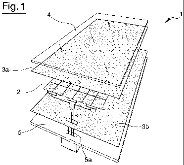
Figure 1 is a perspective exploded view of the photovoltaic module of the
present invention;
Figure 2 is a schematic view of a section of a photovoltaic module according
to the present invention.
Disclosure of Invention
With reference to the figures of the drawings, 1 denotes in its entirety a
photovoltaic module according to the present invention.
The photovoltaic panel 1 comprises a plurality of photovoltaic cells 100
which are electrically interconnected to define a photo-active surface 2. The

CA 02682355 2009-09-29
WO 2008/132764 PCT/IT2007/000306
-4-
electrical interconnection of the photovoltaic cells 100, interconnected in a
lattice, is preferably realised using a grid made of a conductor material,
each
cell being connected to the adjacent cells by metallic connectors commonly
known as ribbons.
The totality of cells and ribbons is closed between a front covering layer 3a
and a back covering layer 3b. Further, the front covering layer 3a is
frontally
covered by a frontal covering element 4, while the back covering layer 3b is
supported posteriorly by a support element.
The covering layers 3a, 3b are made of an insulating material, a.s their main
1o function is to electrically isolate the lattice of photovoltaic cells 100.
It is,
however, also important for the covering layers 3a, 3b to seal the
photovoltaic
cells in order to eliminate risks of corrosion. The layers 3a, 3b
advantageously also function as bonds with respect to the frontal covering
element 4 and the support element.
Finally, and importantly, at least the front covering layer 3a should be
transparent in order to be penneable to the, photons, which when frontally
striking the device must encounter no obstacles- to reaching the photoactive
surface 2.
To satisfy the above requirements, covering layers 3a, 3b made of inert resin
glue are advantageously used, preferably made of EVA (vinyl-ethyl acetate).
EVA is a monomer which when brought to a temperature of 150/160 C
polymerises, sealing the cell lattice internally and performing the above-
cited
bonding action between the elements making up the module. EVA is
transparent after polymerisation. Polymerisation is preferably done in a
2 5 hermetic environment in order to prevent formation of air bubbles
internally
of the covering layers 3a, 3b. The thickness of the covering layers 3a, 3b is
in
the preferred embodiment of about half a millimetre.

CA 02682355 2009-09-29
WO 2008/132764 PCT/IT2007/000306
-5-
The front covering layer 3a is frontally covered by the frontal covering
element 4, which has the function of mechanically protecting the photovoltaic
cells 100 behind it. Generally the frontal covering element 4 is made of
tempered glass which must be able to ensure good mechanical resistance and
excellent light transmission. The thickness of the frontal covering element 4
is preferably comprised between 3.2 and 8 millimetres.
The support element is advantageously constituted by a ceramic slab 5 of
limited thickness. The fact that the slab is made of a ceramic material gives
it
an appearance which achieves a homogeneous effect when the slab is used in
1o context with other commonly-used materials in the field -of construction.
Further, the limited thickness of the slab means that overall the device is
not
unwieldy and facilitates transport and installation. The ~ ceramic slab 5
preferably has a thickness not greater than 3 millimetres and not less than a
millimetre and a half. .The ceramic slab 5 is preferably made of vitrified
ceramic powders, realised by firing a slab-shaped body obtained by ceramic
powder pressing. At least two holes '5a can be_~.nade in the .ceramic slab 5
in
order to pass -the electrical connect'ions for- the panel through. - Vitrified
ceramic is an excellent material for the purpose, as it fully satisfies the
requisites of cheapness, electrical resistance to environmental conditions, as
well as having the required low coefficient of thermal dilation.
The main 'dimensions of the ceramic slab 5 and consequently those of the
whole photovoltaic module 1 can be even very large, resulting in an extensive
surface area of the slab. Preferably the main dimensions of the ceramic slab 5
are 3 metres in length by one metre in width.
The considerable surface obtained represents an advantage with respect to the
prior art, according to which it is nonnally difficult to produce panels
having

CA 02682355 2009-09-29
WO 2008/132764 PCT/IT2007/000306
-6-
large dimensions using Tedlar glass having active elements made of silicon
wafer.

Representative Drawing
A single figure which represents the drawing illustrating the invention.
Administrative Status

2024-08-01:As part of the Next Generation Patents (NGP) transition, the Canadian Patents Database (CPD) now contains a more detailed Event History, which replicates the Event Log of our new back-office solution.

Please note that "Inactive:" events refers to events no longer in use in our new back-office solution.

For a clearer understanding of the status of the application/patent presented on this page, the site Disclaimer , as well as the definitions for Patent , Event History , Maintenance Fee  and Payment History  should be consulted.

Event History

Description Date
Inactive: First IPC assigned 2015-12-18
Inactive: IPC assigned 2015-12-18
Inactive: IPC expired 2014-01-01
Inactive: IPC removed 2013-12-31
Deemed Abandoned - Failure to Respond to Maintenance Fee Notice 2013-04-26
Inactive: Dead - RFE never made 2013-04-26
Application Not Reinstated by Deadline 2013-04-26
Inactive: Abandon-RFE+Late fee unpaid-Correspondence sent 2012-04-26
Inactive: Cover page published 2009-12-08
Inactive: Notice - National entry - No RFE 2009-11-16
Inactive: First IPC assigned 2009-11-13
Application Received - PCT 2009-11-12
National Entry Requirements Determined Compliant 2009-09-29
Application Published (Open to Public Inspection) 2008-11-06

Abandonment History

Abandonment Date Reason Reinstatement Date
2013-04-26

Maintenance Fee

The last payment was received on 2012-04-03

Note : If the full payment has not been received on or before the date indicated, a further fee may be required which may be one of the following

  • the reinstatement fee;
  • the late payment fee; or
  • additional fee to reverse deemed expiry.

Please refer to the CIPO Patent Fees web page to see all current fee amounts.

Fee History

Fee Type Anniversary Year Due Date Paid Date
MF (application, 2nd anniv.) - standard 02 2009-04-27 2009-09-29
Basic national fee - standard 2009-09-29
MF (application, 3rd anniv.) - standard 03 2010-04-26 2010-03-24
MF (application, 4th anniv.) - standard 04 2011-04-26 2011-03-23
MF (application, 5th anniv.) - standard 05 2012-04-26 2012-04-03
Owners on Record

Note: Records showing the ownership history in alphabetical order.

Current Owners on Record
SYSTEM S.P.A.
Past Owners on Record
FRANCO STEFANI
Past Owners that do not appear in the "Owners on Record" listing will appear in other documentation within the application.
Documents

To view selected files, please enter reCAPTCHA code :


To view images, click a link in the Document Description column. To download the documents, select one or more checkboxes in the first column and then click the "Download Selected in PDF format (Zip Archive)" or the "Download Selected as Single PDF" button.

List of published and non-published patent-specific documents on the CPD .

If you have any difficulty accessing content, you can call the Client Service Centre at 1-866-997-1936 or send them an e-mail at CIPO Client Service Centre.


Document
Description 
Date
(yyyy-mm-dd) 
Number of pages   Size of Image (KB) 
Abstract 2009-09-29 1 73
Description 2009-09-29 6 259
Drawings 2009-09-29 1 49
Claims 2009-09-29 2 54
Representative drawing 2009-12-08 1 35
Cover Page 2009-12-08 2 68
Notice of National Entry 2009-11-16 1 194
Reminder - Request for Examination 2011-12-29 1 118
Courtesy - Abandonment Letter (Request for Examination) 2012-08-02 1 164
Courtesy - Abandonment Letter (Maintenance Fee) 2013-06-21 1 173
PCT 2009-09-29 2 74
Fees 2010-03-24 1 36
Fees 2011-03-23 1 36