Note: Descriptions are shown in the official language in which they were submitted.
CA 02682986 2009-10-05
WO 2008/124438 PCT/US2008/059138
ACOUSTO-OPTIC DEVICES HAVING EXTENDED TEMPERATURE
RELIABILITY
The present invention relates generally to optical modulation systems
and related components, and more particularly, to acousto-optical modulators
and
similar devices that modulate light beams using the acousto-optic effect.
Acousto-optic modulators, sometimes referred to as Bragg cells,
diffract and shift light using sound waves at radio frequency. These devices
are often
used for Q-switching, signal modulation in telecommunications systems, laser
scanning and beam intensity control, frequency shifting, and wavelength
filtering in
spectroscopy systems. Many other applications lend themselves to using acousto-
optic devices.
In such acousto-optic devices, a piezoelectric transducer, sometimes
also referred to as an RF transducer, is secured to an acousto-optic bulk
medium as a
transparent optical material, for example, fused silica, quartz or similar
glass material.
An electric RF signal oscillates and drives the transducer to vibrate and
create sound
waves within the transparent medium which effect the properties of an optical
field in
the medium via the photo elastic effect, in which a modulating strain field of
an
ultrasonic wave is coupled to an index of refraction for the acousto-optic
bulk
medium. As a result, the refractive index change in amplitude is proportional
to that
of sound.
The index of refraction is changed by moving periodic planes of
expansion and compression in the acousto-optic bulk material. Incoming light
scatters because of the resulting periodic index modulation and interference,
similar to
Bragg diffraction.
A piezoelectric transducer can create the sound waves and the light
beam is diffracted into several orders. It is possible to vibrate a bulk
medium with a
sinusoid signal and tilt the acousto-optic modulator such that light is
reflected from
flat sound waves into a first diffraction order to result in a high deflection
efficiency.
In acousto-optic devices, light can usually be controlled by: 1)
deflection, 2) intensity, 3) frequency, 4) phase, and 5) polarization.
-1-
CA 02682986 2009-10-05
WO 2008/124438 PCT/US2008/059138
In acousto-optic systems using deflection, a diffracted beam emerges at
an angle depending on the wavelength of the light relative to the wavelength
from the
sound. When controlling light by intensity, however, the amount of light
diffracted
by sound depends on the intensity of the sound to modulate the intensity of
the light in
the diffracted beam. With frequency control over the light, the frequency of
the
diffracted beam is Doppler-shifted by an amount equal to the frequency of the
sound
wave, as compared to Bragg diffraction, in which light is scattered from
moving
planes. The frequency shift can also occur because the energy and momentum of
photons and phonons is conserved. Frequency shifts can vary from as little as
20
MHz to as much as 400 MHz or with even greater ranges in some cases. Two
acoustic waves can travel in opposite directions in the material and create a
standing
wave, which does not shift the frequency. In systems controlling light using
phase,
the diffracted beam can be shifted by the phase of the sound wave. In systems
controlling light by polarization, collinear transversal acoustic waves are
perpendicular along longitudinal waves to change polarization. Thus, there
could
occur a birefringent phase-shift.
Acousto-optic modulators are preferred in many applications because
they are faster than tiltable mirrors and other mechanical devices. The time
it takes
for the acousto-optic modulator to shift an exiting optical beam is limited to
the transit
time of the sound wave. The acousto-optic modulators are often used in Q-
switches
where a laser produces a pulsed output beam at high peak power, typically in
the
Gigawatt range. This output could be higher than lasers operating a continuous
wave
(CW) or constant output mode.
Examples of acousto-optic modulator devices and similar acousto-
optic systems are disclosed in commonly assigned U.S. Patent Nos. 4,256,362;
5,923,460; 6,320,989; 6,487,324; 6,538,690; 6,765,709; and 6,870,658, the
disclosures which are hereby incorporated by reference in their entirety.
Conventional acousto-optic devices typically rely on the use of large
and costly hybrid output radio frequency (RF) amplifiers to provide the
requisite drive
power necessary for use in operation of the device. Usually a higher supply
voltage is
-2-
CA 02682986 2009-10-05
WO 2008/124438 PCT/US2008/059138
applied in order to accommodate the requisite output intercept point of the
hybrid
output radio frequency amplifiers. This results in the use of additional
and/or more
costly power supplies to meet both the integrated circuit (IC) and radio
frequency
amplifier requirements.
In other applications of conventional acousto-optic devices, the designs
typically incorporate one or more monolithic piezoelectric platelets, which
are bonded
to the bulk medium for launching an ultrasonic strain field into the bulk
medium. In
some examples, a low compliance alloy bond fuses the two components together
providing an interface, which results in lower acoustic losses, while
accommodating
broadband impedance matching between the platelet and the optical, bulk
medium.
The combination of different coefficient-of-thermal expansion (CTE) for the
platelet
and optical medium, coupled by the low compliance interface, may lead to
stress
causing localized shear CTE expansion mismatch induced fracture and failure of
large
platelet acousto-optic devices subjected to extended temperature conditions.
These
extended temperature conditions may occur both in a non-operable state, i.e.,
at a
survivability storage temperature, or in some cases as a result of high-level
signal
conditions.
Some critical applications using acousto-optic devices modulate the
intensity of an optical beam. This modulation can create small deviations in
the
output angle of the diffracted beam because of the local thermal transients
introduced
when the RF modulation waveform to the device is turned ON and OFF. These
thermal transients can negatively impact the resolution of the focused spot,
which can
be produced.
An acousto-optic modulator includes an acouto-optic bulk medium and
transducer attached to the acousto-optic bulk medium. The transducer includes
an
electrode circuit and plurality of piezoelectric platelet segments attached to
the bulk
medium and supporting the electrode circuit. A ground plane is positioned
between
the piezoelectric platelet segments and the acousto-optic bulk medium. The
platelet
segments are generated without separating or otherwise affecting the common
ground
metal between the individual platelet segments and the acousto-optic bulk
medium.
-3-
CA 02682986 2009-10-05
WO 2008/124438 PCT/US2008/059138
The piezoelectric platelet segments are configured for reducing shear stress
and
susceptibility to fracture due to temperature extremes.
The electrode circuit can be formed as a linear array electrode such that
each piezoelectric platelet segment supports a respective electrode. The
transducer
driver can be formed by a plurality of amplifiers connected to the electrodes
such that
each electrode is driven by a respective single amplifier to impart beam
steering.
Each amplifier is preferably formed in one aspect of the present invention as
a
monolithic microwave integrated circuit (MMIC). The transducer driver can
establish
the amplitude and phase of each waveform imparted by an electrode.
In yet another aspect, a direct digital synthesizer (DDS) circuit can
output arbitrary waveforms to each platelet segment, to provide individual
phase and
amplitude control can be performed. The DDS circuit can be formed as a phase
accumulator and one or more discrete memory devices and digital-to-analog
converters. The phase accumulator could be formed as a complex programmable
logic device to provide address generation for the various memory devices.
Each
digital-to-analog converter (DAC) is connected to up to 10 bits of a given
memory
device output prior to filtering and input to each amplifier. As a result, one
128-bit
Dynamic Random Access (DRAM) Memory Bank can provide 12 discrete output
channels, which support individual phase and amplitude offsets to each
respective
transducer platelet segment.
Other objects, features and advantages of the present invention will
become apparent from the detailed description of the invention which follows,
when
considered in light of the accompanying drawings in which:
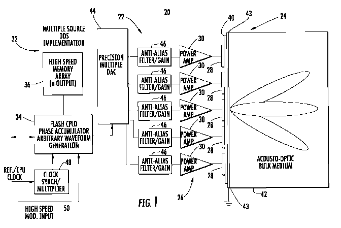
FIG. 1 is a high-level block diagram of an acousto-optic modulator
using a linear electrode array for a transducer in accordance with a non-
limiting
example of the present invention.
FIG. 2 is a graph showing the acoustic spectrum performance, which
results for the transducer and linear electrode array in accordance with the
non-
limiting example shown in FIG. 1.
-4-
CA 02682986 2009-10-05
WO 2008/124438 PCT/US2008/059138
FIG. 3 is a graph showing phase in degrees relative to an emitter phase
step and frequency for the acousto-optic modulator using the linear electrode
array
shown in FIG. 1, in accordance with a non-limiting example of the present
invention.
FIG. 4 is a high-level block diagram of another embodiment of an
acousto-optic modulator similar to FIG. 1 and showing a segmented
piezoelectric
platelet array attached to the ground plane and acousto-optic bulk medium in
accordance with a non-limiting example of the present invention.
FIGS. 5 and 6 are fragmentary views showing the piezoelectric platelet
before reduction and after reduction to form the segmented piezoelectric
platelet in
accordance with a non-limiting example of the present invention.
FIGS. 7 and 8 are fragmentary diagrams showing respective non-
interdigitated and interdigitated drive connections for RF modulation and
pulse
optical intensity modulation allowing bi-phase RF modulation of an acousto-
optic
modulator in accordance with a non-limiting example of the present invention.
FIG. 9 is a graph showing results of the bi-phase RF modulation on the
acousto-optic modulator and showing the acoustic axis and optical axis in
accordance
with a non-limiting example of the present invention.
FIG. 10 is a graph showing the results of phase modulation on the
acousto-optic modulator in accordance with a non-limiting example of the
present
invention.
Different embodiments will now be described more fully hereinafter
with reference to the accompanying drawings, in which preferred embodiments
are
shown. Many different forms can be set forth and described embodiments should
not
be construed as limited to the embodiments set forth herein. Rather, these
embodiments are provided so that this disclosure will be thorough and
complete, and
will fully convey the scope to those skilled in the art. Like numbers refer to
like
elements throughout.
FIG. 1 is a block diagram of an acousto-optic modulator 20 and
showing a transducer driver 22 for an acousto-optic device 24 as an acousto-
optic
modulator in accordance with a non-limiting example of the present invention.
The
-5-
CA 02682986 2009-10-05
WO 2008/124438 PCT/US2008/059138
acousto-optic modulator 20 shown in FIG. 1 overcomes the disadvantages of
conventional acousto-optic modulators that rely on large and costly hybrid
output RF
amplifiers to provide a requisite drive power necessary for useful operation
of the
device. In these prior art devices, a higher supply voltage than is typically
used for a
majority of the circuitry is normally required to accommodate the requisite
output
intercept point of hybrid output RF amplifiers. This results in one or both of
additional and more costly power supplies to meet the power requirements and
supply
voltages of the driver integrated circuits (IC's) and RF amplifier output.
Current approaches for providing the RF driving excitation for
operation of an acousto-optic modulator and/or similar device typically rely
on the use
of hybrid RF amplifiers to supply sufficient RF power to a common
piezoelectric
electrode used in a conventional acousto-optic modulator in order to operate
properly.
The total RF drive power requirement is determined by the characteristics of
the
acousto-optic interaction being sought, which in turn determines the amplitude
and
geometric extent of the strain field that must be produced in the interaction
medium.
In many acousto-optic modulators, the emitter (i.e., electrode) drive
power and operating carrier frequencies largely precluded the use of
traditional video
IC components used with pulsed, ultrasound imaging systems. Acousto-optic
devices
typically required low impedance linear sources that were capable of sourcing
significantly more current than for diagnostic ultrasound imaging array
applications.
In the embodiment of the invention described here, the use of low cost
monolithic RF
(MMIC) components in conjunction with a transducer array is required to
produce the
requisite optical phase retardation consistent with emitter power and
impedance
considerations. Other phased array approaches for acousto-optic devices have
focused on the acousto-optic interaction benefits obtained in terms of
increased
bandwidth and efficiency using a conventional RF amplifier system to drive a
transducer array.
In accordance with a non-limiting example of the present invention, a
piezoelectric oscillator, e.g., transducer, is formed as an electrode
structure 26 (FIG.
1) and is broken into a discrete linear array of individual electrodes 28,
also generally
-6-
CA 02682986 2009-10-05
WO 2008/124438 PCT/US2008/059138
termed emitters. Each individual electrode 28 is driven by a low cost,
monolithic RF
amplifier 30 as illustrated. The number of electrodes 28 is typically
determined to be
consistent with a suitable radiation resistance, so as to limit the maximum
element
drive power required to facilitate the use of a plurality of monolithic output
RF
amplifiers.
Because the interaction between the light and sound is an integrated
effect, the amplitude of the phase retardation produced in the optical field
is
equivalent to the use of a single large transducer so long as all emitters,
i.e.,
electrodes, maintain a high degree of synchronism. Because each amplifier
supplies
only a fraction of the necessary RF power, the supply voltage is also reduced
by
approximately the square root of the number of emitters, i.e., electrodes. In
addition,
the total capacitance of the conventional transducer electrode no longer
becomes a
limiting factor in the length of the interaction region that can be used,
because the
capacitance and corresponding radiation resistance of the array elements are
now
independent of the total interaction length.
An extension of this linear drive system is provided by the plurality of
monolithic amplifiers 30, when used in conjunction with a direct digital
synthesizer
(DDS) circuit as a drive controller, illustrated generally at 32, which can
set both the
amplitude and phase of each emitter drive waveform in real time. By using low
cost
DDS IC components, or a dedicated phase accumulator 34 and high speed memory
circuit 36, precise phase and amplitude adjustments may be made to each
electrode
28, allowing the majority of acoustic energy to be directed into a single,
steerable,
boresight radiation lobe. This maintains phase matching between the incident
light
and sound field and achieves significant gains in scattering efficiency,
deflection
linearity, and high resolution tunable filtering. The acousto-optic modulator
20 may
also implement phase only modulation of light intensity, as will be explained
below.
Some systems using phased array approaches for acousto-optic
devices, have addressed these benefits using conventional single drive
approaches,
resulting in partial phase matching via one of two principal radiation lobes,
or by
using bi-phase emitter excitation into one principal lobe using a difficult
blazing
-7-
CA 02682986 2009-10-05
WO 2008/124438 PCT/US2008/059138
process. Neither approach addresses the drive methodology nor impedance
limitations imposed by large arrays. These systems also do not address the
ability to
steer and provide real time correction of phase errors introduced by the drive
circuitry,
dedicated phase only modulation of light intensity, and angular compensation
for
acoustic anisotropy. They do not address non-linear scan versus frequency
artifacts
introduced by geometric imperfections in the optical system.
The system 20, in accordance with a non-limiting example of the
present invention, uses a plurality of monolithic RF amplifiers 30 in
conjunction with
a linear electrode array 26, to offer a lower cost implementation and provide
the
requisite RF drive waveform for aousto-optic applications, while also reducing
the
necessary supply voltage and increasing overall reliability.
The driver 22 adjusts the phase and amplitude of the RF drive
waveform to allow weighting and steering of a single, principal acoustic
radiation
lobe and provide enhanced bandwidth, scattering efficiency, phase-only
modulation.
It also corrects for phase errors and non-ideal scan artifacts inherent in the
system
hardware.
The driver 22 as described can be applied directly to the design of
acousto-optic modulators and related components, including those systems used
by
semiconductor mask equipment vendors, original equipment manufacturers (OEM)
for laser equipment, and different technology and government customers. It can
be
used in the development of high resolution and low power acousto-optic tunable
filters (AOTF).
Referring again to FIG. 1, more detailed components of the acousto-
optic modulator 20 are explained. The acousto-optic device 24 includes the
linear
electrode array 26 positioned on a monolithic piezoelectric platelet 40 in
this example
and acousto-optic bulk medium 42. The electrodes 20 are formed in a linear
array on
the piezoelectric platelet 40, which connects to the acousto-optic medium bulk
42 via
a ground plane 43. The phase accumulator 34 can be formed as a flash complex
programmable logic device (CPLD) and is operative as a phase accumulator and
arbitrary waveform generator. It inputs signals to the high speed memory array
36
-8-
CA 02682986 2009-10-05
WO 2008/124438 PCT/US2008/059138
having an n-output, wile also inputting signals to a precision, multiple
digital-to-
analog converter (DAC) 44 as illustrated. Typically, the flash CPLD 34 can be
formed from macro cells that contain logic for implementing disjunctive
expressions
or more specialized logic. It could be formed from programmable array logic
(PLA)
circuits and field programmable gate array (FPGA) circuits.
The DAC 44 inputs to a plurality of anti-alias filter/gain circuits 46,
each connected to a monolithic power amplifier 30 and respective electrode 28,
as
explained before. The electrodes 28 form a discrete linear array that connects
to the
piezoelectric platelet 40 and acousto-optic bulk medium 42. Thus, each
electrode is
driven by a low cost monolithic RF amplifier. A system clock may be used in
conjunction with a clock synchronizer and multiplier circuit 48 to provide the
requisite clock signal to the CPLD 34, which also receives a signal as a high-
speed
modulator input 50.
Each power amplifier 28 could be formed as a high performance
MMIC amplifier, such as a Sirenza micro device SBB-2089Z circuit. This device
is a
high performance InGaP HBT MMIC amplifier using a Darlington configuration and
active bias network to provide stable current over temperature and process
beta
variations. It can operate from a 5V supply. It does not require a dropping
resistor as
compared to typical Darlington amplifiers. It has high linearity 5V gain block
applications that require small size and minimal external components. It is
internally
matched to 50 ohms.
The circuit can operate from about 50-850 MHz and is cascadable and
active biased. It is available in lead free, RoHS compliant packaging with
IP3=42.8
dBm @ 240 MHz. Other specifications include: (a) P1dB=20.8 dBm @ 500 MHz;
(b) single fixed 5V supply; (c) robust 1000V ESD, class 1 C; (d) low thermal
resistance; and (e) MSL 1 moisture rating.
It should be understood that the direct digital synthesis (DDS) circuit
could include different components than those illustrated, but basically would
include
a clock, phase accumulator, memory and DAC. In some implementations such as
for
application to the bi-phase RF Modulation technique described below, a dual
channel
-9-
CA 02682986 2009-10-05
WO 2008/124438 PCT/US2008/059138
or two single DDS IC's may be used in conjunction with one or more clock
distribution buffer IC's, to form two separate interdigitated linear
transducer array's,
so that the phase of each array may be changed in a manner described below. In
discrete implementations of the RF driver which support the use of multiple
low cost
MMIC amplifiers feeding a transducer array as described, an electronic
controller or
other system could fill the memory with data, with each data item representing
the
amplitude of the signal as a binary word at an instant of time. A counter as a
phase
accumulator can advance by increments on each pulse from a frequency
reference,
and output as the phase, to select each item in a data table. The DAC will
convert this
sequence of data to an analog waveform.
It should also be understood that individual integrated circuits (IC's)
can be used with elements integrated into individual core chip functions and
use
multiple chips. Any synthesizers would be synchronized with respect to the
common
clock synchronizer and multiplier 48. The power amplifiers 30 could be
distributed
and used as a phased array and coherent approach to provide multiple coherent
RF
sources. It is also possible to use a plurality of direct digital synthesizers
as integrated
circuits or a combination, all deriving their common core logic from a common
clock.
FIGS. 2 and 3 are graphs showing the acoustic spectrum and adjacent
element drive phase performance of the acousto-optic modulator 20 illustrated
in FIG.
1. As noted before, the modulator 20 uses low cost monolithic amplifiers,
which are
nominally matched to a load which has a radiation impedance defined by an
electrode.
The total array size is no longer limited by the total capacitance of the
transducer, as
the radiation impedance may be tailored by choosing an appropriate element
size. As
a result, there is no requirement to section or flip the electrodes to raise
the overall
radiation resistance to improve the electrical bandwidth capability of the
device.
Beam steering can be effected to maintain phase matching between the light and
sound field with an order of magnitude increase in scattering efficiency
obtainable in
some cases. Improvements in narrow band spectral filtering are achievable and
bi-
phase RF modulation as described below for thermal control is possible. The
system
has a higher reliability and simplified design than some available designs.
-10-
CA 02682986 2009-10-05
WO 2008/124438 PCT/US2008/059138
FIG. 2 is a graph that illustrates the beam steering inside the crystal as
the acousto-optic bulk medium that occurs by changing the phase of the
individual
electrodes produced by the DDS drive circuit 22. The driver as illustrated and
described above can be used to steer the beam around the acousto-optic bulk
medium.
The dashed line to the right of the zero radiance line illustrates the
function as
described with the beam steering.
FIG. 3 is a graph that shows a typical value for the phase change
between adjacent electrodes that must be applied at a given frequency to keep
the
beam matched between the light and sound field.
FIGS. 4-6 illustrate an acousto-optic modulator that extends the
temperature reliability of such system and enhances survivability under harsh
environments using a segmented (transducer) piezoelectric platelet. Common
elements as described relative to FIG. 1 are given the same reference numeral
with
reference to FIGS. 4-6.
Conventional acousto-optic devices typically incorporate one or more
monolithic piezoelectric platelets, which are bonded to the suitable
transparent bulk
medium for launching the ultrasonic strain field into the bulk medium. These
platelets are formed using materials typically known to those skilled in the
art.
Usually, a low compliance alloy bond fuses the two components together to
provide
an interface, which results in low acoustic losses while accommodating
broadband
impedance matching between the platelet and optical bulk medium. A ground
plane
is typically included. The combination of different coefficient of thermal
expansion
(CTE) for the platelet and optical bulk medium, coupled by the low compliance
interface, may lead to stress, creating localized shear CTE mismatch, and
resulting in
fracture and failure of large platelets and acousto-optic devices when
subjected to
extended temperature conditions. These extended temperature conditions may
occur
both in a non-operable state, i.e., at a survivability storage temperature, or
as a result
of high-level signal conditions.
Some prior art approaches for extending the survivability temperature
of these acousto-optic devices during non-operating storage conditions use
active
-11-
CA 02682986 2009-10-05
WO 2008/124438 PCT/US2008/059138
thermal resistance heaters or thermoelectric peltier devices to limit the
temperature
variation seen by critical device interfaces. Similar approaches, in
conjunction with
careful passive thermal design, are also used during active operation of the
device to
minimize the temperature extreme at which the transducer is allowed to
operate.
The modulator shown in FIGS. 4-6 has the monolithic piezoelectric
transducer platelet broken into an array of segmented piezoelectric "tiles"
50. Fine
cuts 51 made in the polished piezoelectric transducer platelet prior to
bonding appear
as individually bonded "tiles" 50 after reduction of the platelet to the
proper resonant
thickness as shown in FIG. 6. It should be understood that the electrodes
could be
individually driven as an array or electrically connected together and driven
as a
single monolithic transducer.
Because the total differential elongation which would normally occur
at the free boundary between transducer platelet elements and the substrate as
the bulk
medium is smaller by virtue of a reduction in the individual lateral
dimensions of the
transducer segments, the constrained boundary produced by the vacuum alloying
of
metals, builds up a smaller amount of shear stress when compared with the
larger
conventional transducer structure. As a result, the fracture limit of these
crystalline
materials is less likely to be reached at a given temperature extreme than
that at which
the bond was formed.
This approach to extending the temperature reliability of the acousto-
optic device is passive in nature, requiring no active system during storage
to enhance
survivability over extremes in the ambient temperature, which may be
encountered.
Also, higher power applications which reduce the lifetime of the device bond
due to
thermally generated stress, related fracture, and bond delamination may also
benefit
from the reduction in the magnitude of the total stresses which are generated
at the
bond interface.
This structure can be applied to acousto-optic modulator components,
including various laser cavity devices and medium-powered, air-cooled, Q-
switch
devices. The structure can also be used in space qualification applications.
-12-
CA 02682986 2009-10-05
WO 2008/124438 PCT/US2008/059138
FIG. 4 shows the acousto-optic modulator 20 in which the acousto-
optic bulk medium 42 includes the segmented electrodes 28 and the segmented
piezoelectric "tiles" 50 produced from the transducer platelet. Each electrode
28 and
"tiled" transducer platelet 50 is connected to the respective power amplifier
30,
together with the other circuit components shown in FIG. 1 and represented
generally
by the block 22 corresponding to the power amplifier and driver.
FIG. 5 shows the transducer platelet before reduction, while FIG. 6
shows the transducer platelet after reduction.
By segmenting the transducer platelet, more room is allowed for
differential expansion. The smaller distance fitted by the "tiling" reduces
any "build-
up" of stress. FIG. 5 shows the transducer platelet before reduction such that
the
transducer platelet could be about 0.030 to about 0.040 inches thick before
cutting. It
is possible to predefine or precut the cuts at a depth of about 0.002 to about
0.003
inches thick, i.e., about 50 to about 75 microns, such that the transducer
platelet can
be reduced to a resonant thickness, which is about a half wavelength acoustic
thickness at the frequency of interest. Typically, this could be about 20 to
about 50
microns as the desired thickness. By making the cuts about 50 to about 75
microns
thick when the transducer platelet is reduced as shown in FIG. 6, the cuts
will be at
the desired spacing.
During manufacturing, a large number of potential transducer platelets
could be cut to a depth of about 200 to about 150 microns, or about 0.004
inches, to
ensure that different transducer platelets can be used and reduced to a
resonant
thickness.
It is desirable to cut the transducer platelet before adhering it to a
ground plane or bulk medium because if any cuts are made after the transducer
platelet is adhered, the ground plane could be accidentally cut. It is also
possible to
use an etch ion mill process, a mask or sputter process, and ion beam process
for
small geometries. Harmonic saws could also be used to obtain geometries that
are
about 0.003 to about 0.005 inches.
-13-
CA 02682986 2009-10-05
WO 2008/124438 PCT/US2008/059138
During manufacturing, the ground plane should be protected. It
operates similar to a capacitor in conjunction with other components and
should not
be cut. The size of the gap relative to the size of the platelet can be
important in some
applications. Because sidelobes are generated with acoustic diffraction
patterns,
energy can be removed in angles that are undesirable unless the cuts are small
relative
to the width of the electrode to counter such effects.
FIGS. 7-10 show details of an RF phase modulation technique for
performing acousto-optic intensity modulation of an optical wavefront. In
FIGS. 7
and 8, the electrodes are shown at 28. The transducer platelet 40 and ground
plane 43
are attached to the bulk medium 42 as in FIG. 1.
For some applications using acousto-optic modulation to modulate the
intensity of an optical beam, small deviations in the output angle of the
diffracted
beam are produced by local thermal transients that are introduced when the RF
modulation waveform to the device is turned ON and OFF. These thermal
transients
can negatively impact the resolution of the focused spot produced in
operation.
Current approaches for stabilizing the angular shift that occurs with
conventional RF modulation waveforms rely on localized passive thermal
approaches
to minimize the magnitude and geometric variation of the temperature effects
produced in the crystal, i.e., acousto-optic bulk medium. Active distributed
thin film
heating approaches have also been implemented, which require active monitoring
and
averaging of the input RF drive signal to provide compensatory thermal heating
and
generate a stationary thermal field at the transducer.
In accordance with a non-limiting example of the present invention, a
phase modulated RF waveform of constant RF power imparts the desired optical
modulation to the acousto-optic device, thereby eliminating or greatly
reducing the
generation of thermal transients within the bulk medium associated with
conventional
drive approaches.
The system and method, in accordance with a non-limiting example of
the present invention, uses coherent phasing of the linear electrode array to
alter the
angular momentum distribution of the acoustic field and alternately allow and
inhibit
-14-
CA 02682986 2009-10-05
WO 2008/124438 PCT/US2008/059138
phase matching between the optical and acoustic field. This imparts the
desired
intensity modulation of the optical wavefront. The modulating RF waveform will
be
of constant average envelope power so that thermal transients produced by
standard
ON/OFF keying of the modulation RF waveform can be largely eliminated. The
thermal profile within the acousto-optic bulk medium can remain essentially
stationary as thermal energy generated in the transduction process at each
transducer
electrode is not dependent on the phase of the RF waveform. The effect of heat
sources within the acousto-optic bulk medium due to acoustic attenuation of
the
radiated acoustic wavefront, will largely integrate optically as the average
near field
strain distribution remains essentially stationary.
The system and method can be applied to single and multi-channel
acousto-optic modulators and associated components used in semiconductor
manufacturing and inspection. In particular, the angular deviations have been
characterized and measured in existing 32-channel acousto-optic modulator
devices,
such as the Model H-600 series acousto-optic modulator manufactured by Harris
Corporation of Melbourne, Florida.
FIG. 9 shows a wavevector diagram for isotropic acousto-optic
interaction, where the normal phase matching condition with the transducer
boresight
wavevector is spoiled by applying a 180-degree phase shift between adjacent
transducer elements comprising an ultrasonic transducer array having the
necessary
dimensions to support efficient diffraction of the incident light wave.
FIG. 10 is a graph showing the calculated acoustic wavevector
spectrum for the transducer array when transducer elements are in phase, and
strong
diffraction of the light occurs, and when the alternate element 180 degree bi-
phase
condition is applied, minimizing the acoustic energy which is now phase
matched to
the incident light. By judicious choice of the element spacing and careful
control of
phase errors, the residual level of scattering produced during the "off' state
can be
reduced to an acceptable level, typically 30 dB below the "on" state level.
This
contrast ratio is comparable or better than the level normally produced for AO
modulation due to residual scatter of the optical wavefront by the optical
medium.
-15-
CA 02682986 2009-10-05
WO 2008/124438 PCT/US2008/059138
FIGS. 7 and 8 show a non-interdigitated system (FIG. 7) and the
interdigitated system (FIG. 8). It should be understood that the phase
modulation for
thermal control in both systems will adjust to the phase of alternate
electrodes. As an
acousto-optic transducer, two alternate sections are driven 180 degrees out-of-
phase
to create a specific radiation beam pattern in the acousto-optic bulk medium.
There
could be positive and negative connections as shown in the interdigitated
system and
a third connection as a ground plane connection.
FIG. 9 shows a graph as a K-space diagram. The K momentum
vectors show phase matching. The incident and diffractive optical wave vectors
are
illustrated as K; and Kd in the isotropic, acousto-optic bulk medium. The
isotropic
interaction allows scattering within a circle, resulting in a phase match
between the
light and sound fields.
As shown in FIG. 10, the lobes in the middle about the zero radians are
diminished when the phase of alternate elements in the electrode structure are
driven
180 degrees out of phase with their adj acent neighbors, as shown by the
dashed lines.
As shown at the central portion of the graph in FIG. 10, the energy is reduced
about
30 decibels, acting similar to an ON/OFF scattering mode. Thus, the phase of
alternate electrodes can be applied.
If the entire array were in-phase, the resultant solid lines would show
light scattering. Thus, the system modulates or "turns off' by changing the
phase of
adjacent electrodes in a phased array system as described. This modulation
scheme
directly supports the use of lower cost amplifiers as compared to hybrid
amplifier
systems in which amplifiers are not distributed and may require higher power
field
effect transistors and higher power output stages. This would generally
require
increased heat sink capability to allow heat dissipation. It would also
require higher
operating voltages because the output intercept point of the amplifier has to
be higher.
At the same time, this modulation scheme may be implemented using a set of
conventional hybrid amplifiers with each amplifier driving two interdigitated
transducers, each with independent phase control, to effect modulation of the
optical
beam in the manner described above.
-16-
CA 02682986 2009-10-05
WO 2008/124438 PCT/US2008/059138
An additional benefit of using a plurality of low cost amplifiers to
drive the transducer array involves an improvement in the ability to drive
large
transducers over larger fractional bandwidths. The radiation impedance defined
by
the electrodes is improved because the overall impedance is inversely
proportional to
the capacitance. Thus, by allowing segmented areas as described before, it is
possible
to drive the capacitance down with the smaller area.
-17-