Note: Descriptions are shown in the official language in which they were submitted.
CA 02683871 2009-10-26
SYNCHRONIZER FOR A DATA ACQUISITION SYSTEM
BACKGROUND
It has been shown that defects, such as the presence of faults, discharges,
etc., lead
to catastrophic failure of power equipment, including medium voltage power
cables,
switchgears, distribution blocks, electric motors, transformers, etc. One
particularly type
of defect that causes an abnormal amount of power equipment failure relates to
internal
discharges, known as partial discharge (PD). As generally known in the art,
partial
discharge can occurs within an insulation medium, such as the insulation layer
of a
medium voltage power cable, an insulation component, e.g., bushing, etc., of a
transformer, switchgear, etc. In time, partial discharge, left unattended, may
significantly
deteriorate the insulation medium along with a combination of other factors
such as
thermal cycling, mechanical fatigue, embrittlement, and moisture ingression.
This may
lead to a high concentration of electrical stress at the particular location
and ultimately
voltage breakdown through the insulation medium. Should this occur during a
critical
period, such as during a peak load for a utility or a critical manufacturing
process for a
manufacturing concern, the repercussions in terms of financial losses and
customer
inconveniences can be quite severe.
As stated above, users of expensive medium or high voltage electrical
equipment
(e.g., medium voltage power cables, switchgears, transformers, electrical
motors,
generators, etc.) incur extraordinary expenses when power equipment
unexpectedly fails.
Scheduled maintenance plans are one approach to combat this ongoing problem.
However, scheduled maintenance plans cause users to incur unnecessary costs
when
equipment is found to be functioning satisfactorily after the scheduled
maintenance.
Therefore, diagnostic systems have been developed that have the ability to
predict
failures in medium voltage power cable, switchgears, transformers, etc., and
thus, enables
the equipment user to utilize condition-based maintenance techniques to avert
such
unexpected failures and associated high costs. Some diagnostic systems attempt
to
identify any defect that would result in a system failure and predict the time
required for
these defects to induce the failure in one or more components of the system.
UTLX\33533AP. DOC -I-
CA 02683871 2009-10-26
SUMMARY
This summary is provided to introduce a selection of concepts in a simplified
form that are further described below in the Detailed Description. This
summary is not
intended to identify key features of the claimed subject matter, nor is it
intended to be
used as an aid in determining the scope of the claimed subject matter.
In accordance with aspects of the present disclosure a system is provided for
testing an electrical power system for defects. The electrical power system
transmits
power at a known frequency. The system comprises a test sensor capable of
capacitively
coupling to a live power component of the electrical power system. The test
sensor is
capable of sensing one or more signals transmitted over the electrical power
system. The
system also includes a data acquisition unit capable of storing the signals
sensed by the
test sensor and a synchronizing circuit that allows the data acquisition unit
to synchronize
the storage of the sensed signals to the frequency of the power transmitted
over the
electrical power system.
In accordance with another aspect of the present disclosure a system is
provided
for testing a power system component for defects via a live power cable. The
power
cable transmits power at a known frequency. The system comprises a sensor
capable of
capacitively coupling to the live power cable, wherein the sensor senses one
or more
power cable signals transmitted over the power cable, a data acquisition unit
capable of
storing the power cable signals sensed by the sensor, and a synchronizer
having a
synchronizing circuit that receives the power cable signals sensed by the
sensor and
generates a synchronizing trigger signal for use by the data acquisition unit
to
synchronize the storage of the power cable signals.
In accordance with another aspect of the present disclosure a synchronizer is
provided that comprises at least one battery and a synchronizing circuit that
is powered
by the at least one battery. The synchronizing circuit receives input signals
sensed from
an insulated power cable, processes the signals, and outputs a reference
signal indicative
of a characteristic of the power transmitted by the insulated power cable.
DESCRIPTION OF THE DRAWINGS
The foregoing aspects and many of the attendant advantages of this disclosure
will
become more readily appreciated by reference to the following detailed
description, when
taken in conjunction with the accompanying drawings, wherein:
UTLX\33533APDOC -2-
I I
CA 02683871 2009-10-26
FIGURE 1 is a block diagram of one embodiment of a data acquisition system
formed in accordance with aspects of the present disclosure;
FIGURE 2 is a block diagram of one embodiment of a data acquisition unit
formed in accordance with aspects of the present disclosure;
FIGURE 3 is a block diagram of one embodiment of a synchronizer formed in
accordance with aspects of the present disclosure;
FIGURE 4 is a block diagram of another embodiment of a synchronizer formed in
accordance with aspects of the present disclosure;
FIGURE 5 is a perspective schematic view depicting a sensor formed in
accordance with aspects of the present disclosure capacitively coupled to an
insulated
power cable;
FIGURE 6 is a graph depicting one example of a bandpass filtered sinusoidal
power signal that is inputted into a zero cross detector, and the
corresponding output, or
square wave, of the zero cross detector; and
FIGURE 7 is a block diagram of another embodiment of a data acquisition system
formed in accordance with aspects of the present disclosure.
DETAILED DESCRIPTION
The detailed description set forth below in connection with the appended
drawings where like numerals reference like elements is intended as a
description of
various embodiments of the disclosed subject matter and is not intended to
represent the
only embodiments. Each embodiment described in this disclosure is provided
merely as
an example or illustration and should not be construed as preferred or
advantageous over
other embodiments. The illustrative examples provided herein are not intended
to be
exhaustive or to limit the invention to the precise forms disclosed.
Similarly, any steps
described herein may be interchangeable with other steps, or combinations of
steps, in
order to achieve the same or substantially similar result.
Embodiments of the present disclosure are generally directed to data
acquisition
and/or diagnostic testing equipment, and components thereof, for testing
insulated power
cables, power cable components (e.g., terminations, joints, splices, etc.),
power
equipment (e.g., switchgears, distribution blocks, generators, electric
motors,
transformers, etc.), etc., for defects, such as the presence of faults,
discharges, etc.
Examples of discharges may include internal discharges (e.g., partial
discharge (PD), etc.)
UTLX\33533APDOC -3-
i I
CA 02683871 2009-10-26
and external discharges (e.g., coronas, arcing, etc.). As is known in the art,
when a
discharge occurs, such as PD, high frequency current and voltage pulses
emanate from
the site of the discharge. With regard to PD, for example, this is typically a
symptom of
the presence of insulation defects which should be located and assessed. Once
the defect
is located and assessed, a decision can then be made as to whether the power
cable, power
equipment, etc., should be repaired or replaced.
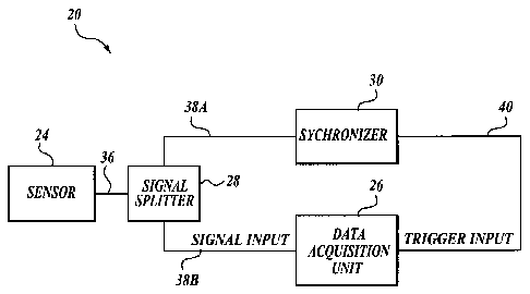
Referring now to FIGURE 1, there is shown a block diagram of one embodiment
of a data acquisition system, generally designated 20, formed in accordance
with aspects
of the present disclosure. The data acquisition system 20 comprises a sensor
24
electrically coupled to a data acquisition unit 26 via a signal splitter 28.
In use, the
sensor 24 senses one or more signals transmitted over a "live" power cable
carrying, for
example, 50 Hz or 60 Hz, medium voltage three phase power. The one or more
signals
are then transmitted to the data acquisition unit 26 to be stored, displayed,
and/or
analyzed.
As will be described in more detail below, the system 20 further includes a
synchronizer 30 that allows the data acquisition unit 26 to synchronize the
storage of the
sensed signals to the frequency of the power transmitted over the tested power
cable C
(FIGURE 5). In one embodiment, the synchronizer 30 provides an accurate phase
angle
reference for accurate phase resolved data acquisition and testing. As used
herein, the
term "live" or "on-line" means that power is presently being transmitted along
the power
cable C. It will be appreciated that power cable C may be configured to carry
one or
more phases (up to three (3) phases) of power to be transmitted between
components.
For example, power cable C may be configured with a single conductor for
carrying only
one phase of a three-phase power feed.
Still referring to FIGURE 1, the components of the data acquisition system 20
will
be described in more detail. In embodiments of the present disclosure, one or
more
components of the system 20 may be designed and constructed so as to be
lightweight,
rugged, waterproof, and otherwise resistant to and protective against the
relatively harsh
operating conditions that would likely be encountered while employed during
field tests,
including, for example, physical shock or impact; dust or other particulate
matter; rain or
other moisture or even submersion; and extreme hot or cold temperatures. As
such,
components, such as the data acquisition unit, the synchronizer, etc., may be
integrally or
UTLX\33533AP.DOC -4-
CA 02683871 2009-10-26
separately housed by a housing that is constructed of an appropriately strong
and durable
yet lightweight material, such as, for example, high impact plastic, and made
substantially
sealable against intrusion by particulates and water.
As briefly described above, the sensor 24 of the system 20 senses one or more
signals traveling, for example, along one or more power cables over a period a
time. The
one or more signals sensed by the sensors 24 (hereinafter referred to as "test
signals")
may include a primary signal component attributable to the frequency of the
power
transmitted thereover, a secondary signal component attributable to faults,
discharges, or
other defects caused by, for example, the power cable, power equipment coupled
to the
power cable, the connections between the power cable and the power equipment,
etc., and
tertiary signal components attributable to noise, interference, etc. The
sensor 24 may be a
portable sensor for in-field data acquisition and/or testing or may be fixed
in place. In the
embodiment shown in FIGURE 5, the sensor 24 is a portable, capacitive signal
probe,
such as a U-shaped metallic (e.g., copper, etc.) probe.
In use, the sensor 24 is capacitively coupled to the power cable C at a
position, for
example, in proximity to where the power cable is terminated (e.g., a
switchgear, an
electrical motor, a transformer, a distribution block, etc.). In that regard,
the sensor 24
may sense test data indicative of faults, discharges, etc., relating to either
the power
cable C or to power equipment connected to a circuit employing the power cable
C. The
sensor 24 may be positioned in other suitable places for sensing test signals
from the
power cable, such as along a portion of the span in proximity to a splice.
Once coupled to
the live power cable, the sensor 24 is capable of obtaining test signals and
transmitting
the test signals to the data acquisition unit 26 via the signal splitter 28
for displaying,
processing, and/or storage, etc.
Still referring to FIGURE 1, the signal splitter 28 is electrically connected
to
sensor 24 via signal cable 36, to the synchronizer 30 via signal cable 38A,
and to the data
acquisition unit 26 via signal cable 38B. In use, the signal splitter 28
receives the one or
more test signals from the sensor 24 and splits the test signals into two,
discrete test
signals of substantially equal bandwidth. The test signals are then
transmitted to the data
acquisition unit 26 and the synchronizer 30.
In one embodiment, the signal splitter 28 may contain circuitry for splitting
the
test signals between two frequency bands, and therefore, may be referred to as
a band
UTLX\33533AP. DOC -5-
I I
CA 02683871 2009-10-26
splitter. In this embodiment, the signal splitter receives the one or more
test signals from
the sensor 24 and splits the test signals into two discrete signals having
different
frequency bands. For example, the signal splitter may be configured to split
or separate
the test signal components into a first group of test signal components having
frequencies
below, for example, 100 KHz and a second group of test signals components
having
frequencies above, for example, 300 KHz. In this way, the primary signal
component
attributable to the power frequency can be separated from the secondary signal
components attributable to faults, discharges, or other defects caused by, for
example, the
power cable, power equipment coupled to the power cable, the connections
between the
power cable and the power equipment, etc. In this embodiment, the first group
of test
signals is transmitted to the synchronizer 30 and the second group of test
signal
components is transmitted to the data acquisition unit 26. It will be
appreciated that the
tertiary components attributable to noise, interference, etc., may be
appropriately split
between the first and second groups according to their frequency
characteristics. It will
be appreciated that the frequency bands stated above are just one example of a
number of
suitable frequency bands that may be practiced with embodiments of the present
disclosure. It will be further appreciated that the signal splitter can be
configured to carry
out further filtering and/or processing, if desired.
Turning now to FIGURE 2, there is shown a block diagram of one embodiment of
the data acquisition unit 26 formed in accordance with aspects of the present
disclosure.
The data acquisition unit 26 comprises an analyzer 42, a processor 44, a
memory 48, a
display 52, and an I/O interface 56 suitably interconnected via one or more
buses 60. The
memory 48 may include read only memory (ROM), such as programmable ROM
(PROM), an erasable programmable ROM (EPROM), and an electrically erasable
PROM
(EEPROM), etc., random access memory (RAM), and storage memory, such as a
solid
state hard drive, a hard drive disc, flash memory, etc. The storage memory
provides
non-volatile storage of computer readable instructions, data structures,
program modules,
and data received from the sensors 24. As used herein, the term processor is
not limited
to integrated circuits referred to in the art as a computer, but broadly
refers to a
microcontroller, a microcomputer, a microprocessor, a programmable logic
controller, an
application specific integrated circuit, and other programmable circuits,
among others.
UTLX\33533AP.DOC -6-
CA 02683871 2009-10-26
The memory 48 depicted in FIGURE 2 is one example of computer-readable
media suited to store data and optional program modules for implementing
aspects of the
present disclosure. As used herein, the term "computer-readable media"
includes volatile
and non-volatile and removable and non-removable memory implemented in any
method
or technology capable of storing information, such as computer-readable
instructions,
data structures, program modules, or other data.
The data acquisition unit 26 may further include an analyzer 42 for analyzing
the
test signals received from the sensor 24 for displaying on the display 52. The
analyzer 42
may be an analog analyzer that analyzes the signals in a time domain, a
digital analyzer
that converts the signals from the time domain to a frequency domain, or an
analog/digital hybrid analyzer. In one embodiment, the analyzer 42 may be a
digital
spectrum analyzer that converts the signals from the time domain into the
frequency
domain by applying a transform, such as a Fast Fourier Transform (FFT). The
signals
may then be displayed on the display 52. In one embodiment, the foregoing
components
of the unit 26 may be housed, for example, in a unitary handheld or hand
carried device.
In use, the test signals sensed by the sensor 24 are received by the signal
splitter 28 and then transmitted to the data acquisition unit 26 via signal
cable 38B
(FIGURE 1), where they are received by signal input 56B of the I/O device 56
(FIGURE 2). The I/O interface 56 then transmits the received test signals to
the
processor 44, which receives the test signals, optionally processes the test
signals, and
stores such signals in the memory 48 for further analysis. In one embodiment,
as will be
described in more detail below, the processor 44 also receives one or more
synchronization signals, for example, a phase reference signal, and based on
the reception
of the synchronization signal, is programmed to synchronize the storage of the
test signals
to the frequency of the power transmitted over the power cable C. The
processor 44 may
also transmit the signals to the analyzer 42 for displaying the signals on the
display 52.
It will be appreciated that the signals received at the signal input 56B may
be
processed by signal processing section 62 prior to arriving at the processor
44 and/or
analyzer 42. For example, the signals may be conditioned by a bandpass filter
and
analog-to-digital converted by an A/D converter. In one embodiment, the
bandpass filter
conditions the test signals such that signals having a frequency of between 1
MHz and
200 MHz pass through for further processing, displaying, and/or storing, etc.
In this way,
UTLX\33533AP DOC -7-
CA 02683871 2009-10-26
the power frequency signal component as well as other unwanted frequency
signal
components will be removed if present from the test signals so as to ease the
recognition
of, for example, the PD signal component or other signal components indicative
of faults,
discharges, etc., potentially present in the signal during subsequent analysis
the stored
signals.
In accordance with aspects of the present disclosure, the system 20 shown in
FIGURE 1 further includes a synchronizer 30 that allows the test signals
stored by the
data acquisition unit 26 to be synchronized to the frequency of the sinusoidal
power
transmitted in the power cable C. In one embodiment, the synchronizer 30
provides one
or more trigger signals to the data acquisition unit so that the data
acquisition unit 26 can
synchronize the storage of the test signals. For example, the synchronizer 30
is capable
of providing a phase angle reference signal as the trigger signal to the data
acquisition
unit 26 for accurate phase resolved data acquisition and testing. In that
regard, the
synchronizer 30 receives the test signals from the signal splitter 28 via
signal cable 38A,
processes the test signals, and transmits phase accurate trigger signals to
the trigger
input 56A of the I/O interface 56 (See FIGURE 2) of the data acquisition unit
26 via
signal cable 40. In response to receiving the trigger signals, the processor
of the data
acquisition unit 26 is capable of synchronizing the storage of the test
signals in its
memory.
Turning now to FIGURE 3, there is shown one embodiment of the
synchronizer 30 formed in accordance with aspects of the present disclosure.
As best
shown in the embodiment of FIGURE 3, the synchronizer 30 includes a
synchronizing
circuit 64 comprised of, for example, an amplifier 66, a filter 68, and a zero
crossing
detector 70. In use, the test signals (or test signal components) outputted by
the signal
splitter 28 are received by the synchronizer 30 at input connector 72, and
passed to the
synchronizing circuit 64, where the signals are amplified by amplifier 66,
bandpass
filtered by the filter 68, and inputted into the zero cross detector 70. In
one embodiment,
the amplifier 66 may limit the frequency response of the amplified test signal
to between
10 Hz and 50 KHz. The bandpass filter 68 to be chosen corresponds to the
frequency of
the power transmitted over the power cable C. For example, in regions that use
60 Hz
power, a 60 Hz bandpass filter (having a width, for example, of about 2 Hz)
would be
used. The bandpass filtered signal then enters the zero cross detector 70,
which
UTL7N3533AP.DUC -8-
i I
CA 02683871 2009-10-26
determines the transitions through zero volts of the sinusoidal bandpass
filtered input
signal, and outputs phase accurate trigger signals at output connector 74 to
be transmitted
via signal cable 40 to the data acquisition unit 26. In one embodiment, the
zero cross
detector 70 converts the inputted sine wave 88 into a square wave 90 and
generates a
trigger signal based on the rising edge 92 of the square wave 90, as best
shown in
FIGURE 6. The trigger signal based on the rising edge 88 is indicative of a
zero degree
phase. Upon receipt of the trigger signal at the trigger input 56A of the unit
26, the
processor 44 begins to store phase resolved signal data in memory 48 for
future analysis.
In one embodiment, the synchronizer 30 may be configured as a portable unit
that
is sized to be carried by hand by a technician and powered by one or more
batteries 78
(e.g., 6-12 VDC). In that regard, the synchronizer 30 may include a protective
housing 76 that envelops the electrical circuitry thereof. The housing 76 can
be
constructed of any suitable lightweight but durable material, such a plastic.
The housing
76 can be a generally box-like shape, although other shapes may be practiced
with
embodiments of the present disclosure. To supply power from the one or more
batteries 78 to the synchronizing circuit 72, the synchronizer 30 may further
include an
on/off switch 80 and a voltage regulation circuit 82. In one embodiment, the
voltage
regulation circuit 82 and the synchronizing circuit 72 may be mounted on a
circuit
board 84 housed within the housing 76.
While the synchronizing circuit 72 has been described above as analog
circuitry
for carrying out the above-described functions, digital circuitry or a
combination of
analog and digital circuitry may also be used. In that regard, referring now
to FIGURE 4,
there is shown a block diagram of another embodiment of a synchronizer 130
formed in
accordance with the present disclosure. As best shown in FIGURE 4, the
synchronizing
circuit 172 of the synchronizer 130 may include a processor 160, a memory 162,
and a
signal processing section 168 suitably interconnected via one or more
communication
buses. As further depicted in FIGURE 4, the synchronizer 130 also include an
I/O
interface 170 for interfacing with, for example, the sensor 24 and the data
acquisition
unit 26, and a trigger signal generator 198. It will be appreciated that the
signals received
at the processor 160 may be processed by signal processing section 168. For
example,
the signals may be conditioned by a bandpass filter, anti-alias filter, etc.,
and are analog-
to-digital converted by an A/D converter. Additionally, it will be appreciated
that the
UTLX\33533AP. DOC -9-
i I
CA 02683871 2009-10-26
trigger signal generator 198 may be part of the synchronizing circuit 172 or
separate
therefrom.
Those skilled in the art and others will recognize that the processor 160
serves as
the computational center of the synchronizer 130 by supporting the execution
of logic,
instructions, etc. either programmed into the processor or available from the
memory 162.
As such, the logic described herein may be implemented in hardware, in
software, or a
combination of hardware and software.
The memory 162 depicted in FIGURE 4 is one example of computer-readable
media suited to store data and optional program modules for implementing
aspects of the
present disclosure. The memory 162 may include read only memory (ROM), such as
programmable ROM (PROM), an erasable programmable ROM (EPROM), and an
electrically erasable PROM (EEPROM), etc., random access memory (RAM), and
storage memory, such as a solid state hard drive, a hard drive disc, flash
memory etc.
The storage memory provides non-volatile storage of computer readable
instructions, data
structures, program modules, etc.
A number of program modules, such as application programs, may be stored in
memory 162, including a phase reference determination module 164. The phase
reference determination module 164 includes logic that instructs the processor
160 to
determine the phase of the power transmitted over the electrical power system
from the
test signals, and in particular, the phase of the power transmitted over the
power cable to
which the sensor 24 is coupled. The logic of the phase reference determination
module 164 further instructs the processor 160 to signal the trigger signal
generator 198
to generate phase accurate trigger signals for output to the data acquisition
unit 26 via
signal cable 40. In one embodiment, the processor, via instructions from the
module 164,
signals the trigger signal generator 198 when the sinusoidal power signal
component of
the signal has a zero degree phase.
Turning now to FIGURE 7, there is shown a block diagram of another
embodiment of a data acquisition system, generally designated 220, formed in
accordance
with aspects of the present disclosure. The data acquisition system 220 is
substantially
similar in construction, materials, and operation as the data acquisition
system 20 of
FIGURE 1 except for the differences that will now be explained in detail. As
best shown
in FIGURE 7, the system 220 further includes an operator activated phase
reference
UTLX\33533AP. DOC -10-
i I
CA 02683871 2009-10-26
selector switch 242. The phase reference selector switch 242 switches between
a first
input that is connected to the signal cable 36 and receives test signals
sensed by the
testing sensor 24T, and a second input that is connected to a signal cable 250
and receives
reference signals sensed by an additional sensor, referred to as the power
phase reference
sensor 24R. The phase reference selector switch 242 outputs either the test
signals or
reference signals to the synchronizing circuit 272 via the signal splitter 28.
Accordingly,
the operator can choose to measure the frequency and/or the phase of the power
transmitted over a power cable with either the test sensor 24T or the
reference sensor
24R, depending on the position of the phase reference selector switch 242.
In one embodiment, the reference sensor 24R can be capacitively coupled to a
preselected insulated power cable at a specific location while the test sensor
24T is used
to sense test data at any number of local power system test points. For
example, in
embodiments where a plurality of insulated power cables terminate at a power
equipment
component, the reference sensor 24R may be capacitively coupled to one of the
power
cables. The test sensor 24T may then be capacitively coupled, one at a time,
to the other
power cables for obtaining test data relating to each power cable. In this
manner, all of
the test points are recorded using a single phase reference. This will aid in
the analysis
when determining the source of the discharge signals.
The principles, representative embodiments, and modes of operation of the
present disclosure have been described in the foregoing description. However,
aspects of
the present disclosure which are intended to be protected are not to be
construed as
limited to the particular embodiments disclosed. Further, the embodiments
described
herein are to be regarded as illustrative rather than restrictive. It will be
appreciated that
variations and changes may be made by others, and equivalents employed,
without
departing from what is claimed. Accordingly, it is expressly intended that all
such
variations, changes, and equivalents fall within what is claimed.
UTLX\33533AP.DOC ' 1 1'