Language selection

Search

Patent 2684256 Summary

Third-party information liability

Some of the information on this Web page has been provided by external sources. The Government of Canada is not responsible for the accuracy, reliability or currency of the information supplied by external sources. Users wishing to rely upon this information should consult directly with the source of the information. Content provided by external sources is not subject to official languages, privacy and accessibility requirements.

Claims and Abstract availability

Any discrepancies in the text and image of the Claims and Abstract are due to differing posting times. Text of the Claims and Abstract are posted:

  • At the time the application is open to public inspection;
  • At the time of issue of the patent (grant).
(12) Patent: (11) CA 2684256
(54) English Title: POWER CONVERTER AND POWER CONVERSION METHOD WITH REDUCED POWER CONSUMPTION
(54) French Title: CONVERTISSEUR D'ALIMENTATION ET PROCEDE DE CONVERSION CONNEXE A FAIBLE CONSOMMATION D'ENERGIE
Status: Granted
Bibliographic Data
(51) International Patent Classification (IPC):
  • H02M 5/458 (2006.01)
  • H05B 41/36 (2006.01)
(72) Inventors :
  • SIMI, VICTOR M. (United States of America)
(73) Owners :
  • LEDVANCE LLC (United States of America)
(71) Applicants :
  • OSRAM SYLVANIA INC. (United States of America)
(74) Agent: SMART & BIGGAR LP
(74) Associate agent:
(45) Issued: 2016-10-04
(22) Filed Date: 2009-11-02
(41) Open to Public Inspection: 2010-05-06
Examination requested: 2014-01-16
Availability of licence: N/A
(25) Language of filing: English

Patent Cooperation Treaty (PCT): No

(30) Application Priority Data:
Application No. Country/Territory Date
12/291,073 United States of America 2008-11-06

Abstracts

English Abstract

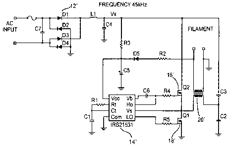
A power converter and power conversion method converts an input AC signal to a voltage usable by a load while reducing power consumption, thereby making the converter and method suitable for a wider range of applications. A rectifier receives the AC input signal and outputs a rectified voltage Vs, a controller has a power input connected to Vs and outputs two out-of-phase signals, two transistors are connected in series between Vs and a ground and each of the two transistors has a gate connected to a respective one of the two out-of-phase signals, and a transformer that has a primary coil connected to a node between the two transistors and a secondary coil connected to a load feeds back current from the secondary coil to the power input of the controller to reduce power consumption.


French Abstract

Un convertisseur dalimentation et un procédé de conversion connexe convertissent un signal alternatif dentrée en une tension utilisable par une charge tout en réduisant la consommation dénergie, rendant ainsi le convertisseur et le procédé appropriés pour une plus grande gamme dapplications. Un redresseur reçoit le signal alternatif dentrée et envoie une tension corrigée Vs, un contrôleur possède une entrée dalimentation connectée à la Vs et envoie deux signaux hors phase, deux transistors sont connectés en série entre des Vs et une mise à la terre, et chacun des deux transistors possède une porte connectée à un des deux signaux hors phase respectifs, et un transformateur doté dune bobine primaire connectée à un nud entre les deux transistors et une bobine secondaire connectée à une charge qui renvoie le courant de la bobine secondaire à lentrée dalimentation du contrôleur afin de réduire la consommation dénergie.

Claims

Note: Claims are shown in the official language in which they were submitted.


I claim:


1. A power converter, comprising:

a rectifier that receives an AC input signal and outputs a rectified voltage
Vs;
a controller whose power input is connected to Vs and that outputs two out-of-
phase signals;

two transistors connected in series between Vs and a ground, each of the two
transistors having a gate connected to a respective one of the two out-of-
phase signals;
and

a transformer having a primary coil connected to a node between the two
transistors and a secondary coil connected to a load and to the power input of
the
controller.

2. The converter of claim 1, wherein the rectifier is a full wave bridge.
3. The converter of claim 2, wherein the rectifier further comprises an
electro-magnetic interference suppression circuit.

4. The converter of claim 1, further comprising a time constant circuit that
is
connected to the controller and that sets a frequency of the two out-of-phase
signals.

5. The converter of claim 1, further comprising a resistor and a capacitor
connected in series between Vs and the ground, and wherein the power input of
the
controller is connected to Vs through a node between the resistor and the
capacitor.

6. The converter of claim 1, wherein the controller is an integrated circuit
with a built-in oscillator and MOSFET driver.


6


7. The converter of claim 1, in a lamp that includes a base and electrodes,
wherein the converter is entirely within the base, wherein the rectifier is
connected to a
lamp terminal on a exterior of the base, and wherein the load is the
electrodes.

8. A power conversion method, comprising the steps of:
rectifying a received AC input signal to output a rectified voltage Vs;

providing Vs to a power input of a controller, the controller outputting two
out-of-
phase signals;

providing each of the two out-of-phase signals to a respective gate of two
transistors connected in series between Vs and a ground; and

in a transformer having a primary coil connected to a node between the two
transistors and a secondary coil connected to a load, feeding back a current
from the
secondary coil to the power input of the controller.

9. The method of claim 8, in a lamp that includes a base and electrodes,
wherein the converter is entirely within the base, wherein the rectifier is
connected to a
lamp terminal on a exterior of the base, and wherein the load is the
electrodes.

10. The method of claim 8, further comprising the step of setting a frequency
of the two out-of-phase signals with a time constant circuit connected to the
controller.
11. The method of claim 8, further comprising the steps of connecting a

resistor and a capacitor in series between Vs and the ground, and connecting
the power
input of the controller to Vs through a node between the resistor and the
capacitor.


7

Description

Note: Descriptions are shown in the official language in which they were submitted.


CA 02684256 2009-11-02
POWER CONVERTER AND POWER CONVERSION
METHOD WITH REDUCED POWER CONSUMPTION
Background of the Invention
The present invention is directed to a power converter and a power conversion
method that supplies a specified power to a load, and more particularly to a
power
converter and power conversion method for a lamp. A power converter receives
an input,
such as a line AC input, and converts the input to a voltage suitable for
operation of the
load.
In some lamps, the voltage suitable for operation is desirably much lower than

line voltage in order to increase efficiency of the lamp. For example,
efficiency of a 120
volt halogen lamp is improved by reducing the operating voltage by a factor of
ten.
Further, it is desirable to integrally include such a converter inside a base
of the lamp.
However, the heat generated by presently available power converters
effectively limits
their applicability to lamps of less than about 30 watts. Since the heat
generated by the
converter relates to the power consumed by the converter, it is desirable to
reduce the
power consumption of the converter.
Summary of the Invention
An object of the present invention is to provide a novel power converter and
power conversion method that avoids the problems of the prior art.
A further object of the present invention is to provide a novel power
converter and
power conversion method in which power is conserved by feeding back a current
from a
1

CA 02684256 2016-01-11
secondary coil of a transformer to a power input of a controller that controls
operation of the
transformer.
According to one embodiment, a power converter, comprising: a rectifier that
receives
an AC input signal and outputs a rectified voltage Vs; a controller whose
power input is
connected to Vs and that outputs two out-of-phase signals; two transistors
connected in series
between Vs and a ground, each of the two transistors having a gate connected
to a respective
one of the two out-of-phase signals; and a transformer having a primary coil
connected to a
node between the two transistors and a secondary coil connected to a load and
to the power
input of the controller.
According to another embodiment, a power conversion method, comprising the
steps
of: rectifying a received AC input signal to output a rectified voltage Vs;
providing Vs to a
power input of a controller, the controller outputting two out-of-phase
signals; providing each
of the two out-of-phase signals to a respective gate of two transistors
connected in series
between Vs and a ground; and in a transformer having a primary coil connected
to a node
between the two transistors and a secondary coil connected to a load, feeding
back a current
from the secondary coil to the power input of the controller.
These and other objects and advantages of the invention will be apparent to
those of
skill in the art of the present invention after consideration of the following
drawings and
description of preferred embodiments.
Brief Description of the Drawings
Figure 1 is schematic diagram of an embodiment of the present invention.
Figure 2 is a diagram showing a circuit suitable for the embodiment of Figure
1.
Figure 3 is a partial cross-section of a lamp including the present invention.
Description of Preferred Embodiments
With reference now to Figure 1, a power converter 10 of the present invention
includes a rectifier 12 that receives an AC input signal and outputs a
rectified voltage Vs, a
controller 14 whose power input is connected to Vs and that outputs two out-of-
phase signals
A, B, two transistors 16, 18 connected in series between Vs and a ground, each
of the two
2

CA 02684256 2016-01-11
transistors having a gate connected to a respective one of the two out-of-
phase signals, and a
transformer 20 having a primary coil connected to a node C between the two
transistors and a
secondary coil connected to a load and to the power input of the controller.
In operation, the controller 14 generates signals A, B that drive transistors
16, 18. The
current that then flows through the primary coil of transformer 20 is changed
by the turns
ratio of the transformer to provide the proper current for the load. The
current feedback from
the secondary coil of the transformer to the power input of the controller 14
provides power to
sustain the operation of the controller during normal operation. This method
of feedback
conserves power, thereby reducing power consumption and heat generated by the
power
converter.
A more particular embodiment is shown in Figure 2. In this embodiment, the
rectifier
12' may be a full wave bridge with diodes D1-D4, and may include an electro-
magnetic
interference (EMI) suppression circuit that includes capacitors C4 and C7 and
inductor Li.
The controller 14' may be an integrated circuit with a built-in oscillator and
3

CA 02684256 2009-11-02
=
MOSFET driver, such as the IR21531 shown. The frequency of the built-in
oscillator
may be set by a time constant circuit that includes resistor RI and capacitor
Cl. The
transistors 16', 18' may be MOSFETs Q1 and Q2 connected to the controller
through
resistors R4-5 and capacitor C6 as shown. The power input Vcc of the
controller may be
connected to Vs through a node between resistor R3 and capacitor C5. In
operation, once
Vs starts to increase, current flows through resistor R3, charging capacitor
C5 until the
clamping action of the controller limits its amplitude, which for a lamp may
be a nominal
15 volts. The primary coil of transformer 20' may be connected to a node
between
capacitors C2 and C3 and the secondary coil may feedback to the power input of
the
controller through resistor R2 and diode D5 as shown. The circuit generates a
high
frequency AC output at the load (e.g., at 12 volts for a lamp) that is
modulated at 120
hertz, for example. The resulting input power factor is very close to unity
(about 0.985 or
better) and the total harmonic distortion is very low.
Figure 3 shows an embodiment wherein the power converter 10 is in a lamp 24
(e.g., a halogen light source) that includes a base 26 and electrodes 28 that
are connected
to a bulb 30, wherein the converter 10 is entirely within the base 26, wherein
the rectifier
is connected to a lamp terminal 32 on a exterior of the base, and wherein the
load is the
electrodes 28. The converter 10 can be packaged as an integral part of the
lamp, and can
operate directly off the AC line input, where the filter reduces both the
conducted and
radiated EMI. By selecting the transformer turns ratio and time constant, the
converter
can operate with 120 or 220-240 volts at both 50 and 60 hertz.
The power converter and power conversion method described herein offers
several advantages. Among those advantages are that the converter includes a
relatively
4

CA 02684256 2009-11-02
. =
simple construction that includes only one integrated circuit so that the
converter can be
low cost and small enough for a lamp base. It operates on a relatively
unfiltered AC
input that generates an output set by the turns ratio of the transformer. This
gives the
converter the ability to be easily adapted to various line voltages. The duty
cycle has
built-in delays to prevent the transistors from overheating due to cross-over
currents. The
frequency of operation of the controller is controlled so the EMI signature is
predictable
and stable at high temperatures. The AC input at the load is a very pure sine
wave with a
power factor close to 1. Further, the feedback from the secondary coil of the
transformer
reduces power consumption and in a lamp limits in-rush current at cold
filament start-up.
While embodiments of the present invention have been described in the
foregoing
specification and drawings, it is to be understood that the present invention
is defined by
the following claims when read in light of the specification and drawings.

Representative Drawing
A single figure which represents the drawing illustrating the invention.
Administrative Status

For a clearer understanding of the status of the application/patent presented on this page, the site Disclaimer , as well as the definitions for Patent , Administrative Status , Maintenance Fee  and Payment History  should be consulted.

Administrative Status

Title Date
Forecasted Issue Date 2016-10-04
(22) Filed 2009-11-02
(41) Open to Public Inspection 2010-05-06
Examination Requested 2014-01-16
(45) Issued 2016-10-04

Abandonment History

There is no abandonment history.

Maintenance Fee

Last Payment of $263.14 was received on 2023-10-19


 Upcoming maintenance fee amounts

Description Date Amount
Next Payment if standard fee 2024-11-04 $624.00
Next Payment if small entity fee 2024-11-04 $253.00

Note : If the full payment has not been received on or before the date indicated, a further fee may be required which may be one of the following

  • the reinstatement fee;
  • the late payment fee; or
  • additional fee to reverse deemed expiry.

Patent fees are adjusted on the 1st of January every year. The amounts above are the current amounts if received by December 31 of the current year.
Please refer to the CIPO Patent Fees web page to see all current fee amounts.

Payment History

Fee Type Anniversary Year Due Date Amount Paid Paid Date
Application Fee $400.00 2009-11-02
Registration of a document - section 124 $100.00 2011-04-15
Maintenance Fee - Application - New Act 2 2011-11-02 $100.00 2011-10-07
Maintenance Fee - Application - New Act 3 2012-11-02 $100.00 2012-10-23
Maintenance Fee - Application - New Act 4 2013-11-04 $100.00 2013-10-29
Request for Examination $800.00 2014-01-16
Maintenance Fee - Application - New Act 5 2014-11-03 $200.00 2014-10-23
Maintenance Fee - Application - New Act 6 2015-11-02 $200.00 2015-10-23
Final Fee $300.00 2016-08-05
Maintenance Fee - Patent - New Act 7 2016-11-02 $200.00 2016-10-19
Registration of a document - section 124 $100.00 2017-02-02
Maintenance Fee - Patent - New Act 8 2017-11-02 $200.00 2017-10-20
Maintenance Fee - Patent - New Act 9 2018-11-02 $200.00 2018-10-19
Maintenance Fee - Patent - New Act 10 2019-11-04 $250.00 2019-10-25
Maintenance Fee - Patent - New Act 11 2020-11-02 $250.00 2020-10-19
Maintenance Fee - Patent - New Act 12 2021-11-02 $255.00 2021-10-19
Maintenance Fee - Patent - New Act 13 2022-11-02 $254.49 2022-10-19
Maintenance Fee - Patent - New Act 14 2023-11-02 $263.14 2023-10-19
Owners on Record

Note: Records showing the ownership history in alphabetical order.

Current Owners on Record
LEDVANCE LLC
Past Owners on Record
OSRAM SYLVANIA INC.
OSRAM SYLVIANA INC.
SIMI, VICTOR M.
Past Owners that do not appear in the "Owners on Record" listing will appear in other documentation within the application.
Documents

To view selected files, please enter reCAPTCHA code :


To view images, click a link in the Document Description column. To download the documents, select one or more checkboxes in the first column and then click the "Download Selected in PDF format (Zip Archive)" or the "Download Selected as Single PDF" button.

List of published and non-published patent-specific documents on the CPD .

If you have any difficulty accessing content, you can call the Client Service Centre at 1-866-997-1936 or send them an e-mail at CIPO Client Service Centre.


Document
Description 
Date
(yyyy-mm-dd) 
Number of pages   Size of Image (KB) 
Representative Drawing 2010-04-12 1 8
Abstract 2009-11-02 1 19
Description 2009-11-02 5 179
Claims 2009-11-02 2 61
Drawings 2009-11-02 2 32
Cover Page 2010-04-28 2 44
Drawings 2016-01-11 2 29
Description 2016-01-11 5 177
Representative Drawing 2016-08-31 1 8
Cover Page 2016-08-31 1 40
Correspondence 2010-11-05 1 12
Correspondence 2010-11-05 1 25
Assignment 2011-04-15 10 540
Assignment 2009-11-02 3 93
Correspondence 2010-10-26 7 346
Correspondence 2015-11-27 5 143
Prosecution-Amendment 2014-01-16 2 78
Examiner Requisition 2015-07-10 3 232
Amendment 2016-01-11 6 205
Final Fee 2016-08-05 2 63
Assignment 2017-02-02 3 123