Note: Descriptions are shown in the official language in which they were submitted.
CA 02684788 2009-10-20
WO 2009/017853 PCT/US2008/061042
RELIABILITY IMPROVEMENT FOR PIEZOELECTRIC
IMAGING ARRAY DEVICE
Cross-Reference to Related Application
This application claims the benefit of priority to U.S. provisional patent
application
serial number 60/913,044, filed on Apri120, 2007.
Field of the Invention
The present invention relates to improving the reliability and image quality
of a
semiconductor imaging device, such as a thin film transistor ("TFT")
piezoelectric imaging
device. TFT's have been used in fingerprint imaging devices to gather
information which
can be provided to a computer, which in turn can create an image of the
fingerprint.
Background of the Invention
Although excellent in imaging ability, semiconductor and/or TFT type
piezoelectric
imaging devices used for fingerprint readers are subject to short life
expectancies. When a
person presents a finger for imaging, electro-static shock, impact, abrasion
and other
deleterious effects are exacted on the imaging device, causing damage to the
imaging device.
Consequently, many prior art semiconductor and/or TFT piezoelectric imaging
devices stop
operating soon after installation.
To extend the life of such devices, the prior art teaches applying insulating
materials
over the top of the imaging devices, thereby protecting the imaging devices.
The prior art
insulating materials provide a physical barrier or static shorting barrier.
However, such
insulating materials reduce the quality of the images produced. Prior art
semiconductor or
TFT imaging devices that have an insulting material produce blurrier images
than those that
do not have the insulting material. Therefore, in order to use a sensitive
device like a
semiconductor or TFT for reading a biological object, such as a fingerprint,
an improved
protective device is needed.
1
CA 02684788 2009-10-20
WO 2009/017853 PCT/US2008/061042
Summary of the Invention
The invention may be embodied as a device for scanning a biological object,
such as a
fingerprint. One such device includes an array of acoustic waveguides and a
piezoelectric
array device. The piezoelectric array devices may be arranged in association
with the
waveguide array to provide ultrasonic energy in the form of an ultrasonic wave
or collection
of waves to the waveguide array, and also arranged to receive ultrasonic
energy in the form
of an ultrasonic wave or collection of waves from the waveguide array. The
acoustic energy
received by the piezoelectric array from the waveguide array may be energy
that has been
reflected from the biological object. A waveguide array according to the
invention uses
internal reflection to transmit the acoustic wave from one end of the
waveguide array to
another end of the waveguide array.
The waveguide array may serve as a platen on which the biological object is
placed
during scanning. An acoustic coupling media may be disposed between the
waveguide array
and the piezoelectric array in order to facilitate transmission of the
acoustic energy traveling
between the waveguide array and the piezoelectric array.
The waveguides of the waveguide array may have a cladding and a core. A
suitable
cladding material may be polymethylmethacrylate. A suitable core material may
be
polystyrene.
Another suitable cladding material may be polyethylene. A suitable core
material
may be polycarbonate.
A device according to the invention may have the piezoelectric array device,
which is
capable of providing ultrasonic energy in the form of an ultrasonic wave or
collection of
ultrasonic waves, and which is capable of receiving reflected ultrasonic
energy in the form of
a reflected ultrasonic wave or collection of ultrasonic waves. An array of
waveguides may be
arranged in association with the piezoelectric array device to receive
ultrasonic energy from
the piezoelectric array device, transmit the ultrasonic energy to a biological
object, receive
ultrasonic energy reflected from the biological object, and transmit the
reflected ultrasonic
2
CA 02684788 2009-10-20
WO 2009/017853 PCT/US2008/061042
energy to the piezoelectric device, where the energy received at the
piezoelectric device is
provided as signals to a computer. The computer may have software running
thereon which
interprets the signals and provides an image of the biological object on a
monitor.
Brief Description Of The Drawings
For a fuller understanding of the nature and objects of the invention,
reference should
be made to the accompanying drawings and the subsequent description. Briefly,
the
drawings are:
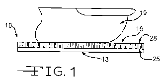
Figure 1 depicts a finger on a device according to the invention;
Figure 2 depicts a top view of a waveguide array that may be used in
a device according to the invention; and
Figure 3 is a perspective view of a device according to the invention.
Further Description of the Invention
Figures 1, 2 and 3 depict a device according to the invention. The device
depicted in
figures 1, 2 and 3 is a fingerprint scanner 10. In such a scanner 10 there may
be an
piezoelectric acoustic detector array 13 and an acoustic waveguide array 16.
The word
"acoustic" is used herein to refer to longitudinal waves, such as ultrasonic
waves, even
though such waves may not be audible by a human being. The detector array 13
may detect
acoustic waves that have been reflected from a biological object, such as a
finger. The
detector array 13 may also produce acoustic waves, and in such a device the
same array may
be used to send acoustic waves toward a finger and also detect the waves
reflected from the
finger. The piezoelectric array 13 depicted in figure 3 includes an array of
TFTs. The
waveguide array 16 depicted in figure 3 insulates the piezoelectric array 13
from electro-
static shock, mechanical shock and/or abrasion that might otherwise be present
if the
biological object were placed directly on the TFT.
In the device depicted in the figures, during operation an ultrasonic pulse
that issues
from the piezoelectric array device 13 is carried to the finger 19 by the
acoustic waveguide
3
CA 02684788 2009-10-20
WO 2009/017853 PCT/US2008/061042
array 16. The ultrasonic waves reflected from the finger 19 travel back via
the same acoustic
waveguide array 16. The reflected waves are detected by the piezoelectric
array device 13.
The waveguide array 16 may be made from glass, plastic, ceramic or metallic
materials. Details of the waveguide array 16 are provided below. Since the
materials of the
acoustic waveguide array 16 act for both electrostatic insulation and as a
shock and abrasion
barrier, the piezoelectric array device 16 is protected, and consequently its
useful life is
extended. However, unlike prior art insulators, the waveguide array 16
produces a much
clearer image of the fingerprint.
The waveguide array 16 may be a bundle of substantially parallel acoustic
waveguides 22 which are held together into a single assembly. Each waveguide
22 may be
fused, bonded or otherwise held rigidly to adjacent waveguides 22. The
waveguide array 16
may take the form of a plate, which can serve as a platen on which the
biological object may
be rested during the scanning process. The acoustic waveguides 22 may be
fibers, and may
be thought of as conduits that transmit acoustic energy from a first end of
the waveguide 22
to a second end of the waveguide 22. Each waveguide 22 in the array 16 may be
used to
convey a different acoustic signal from one side of the array 16 to the other
side. In order to
preserve the information being transmitted by the waveguides 22, the relative
positions of the
first ends of each waveguide may be placed substantially in a first plane, and
the relative
positions of the second ends of each waveguide may be placed substantially in
a second
plane.
Each waveguide 22 may be constructed to have a core 31 and a cladding 34. The
core
31 and cladding 34 are made from different materials so that the speed-of-
sound in the core
31 is different from the speed-of-sound in the cladding 34. In this manner, an
acoustic wave
traveling through the waveguide 22 is substantially contained in the waveguide
22 by means
of total internal reflection at the interface of the two different materials.
Since acoustic energy may be used to transmit information, information about a
fingerprint may be transmitted via the waveguides 22 using ultrasonic energy
pulses. The
4
CA 02684788 2009-10-20
WO 2009/017853 PCT/US2008/061042
waveguide array 16 may be used to transmit information about a pattern (such
as a
fingerprint) from one side of the waveguide array 16 to another side of the
waveguide array
16, without significant loss of the relative proportions of the pattern
information.
The waveguide array 16 may be embodied as a polymer clad fiber, which can be
considered to be an acoustic waveguide 22. Other materials, such as glass,
metal or ceramic,
may be used to clad the fiber. It will be recognized that there is a large
number of
core/cladding combinations that can be successfully be used for the invention.
By carefully
selecting the materials used for the core 31 and cladding 34, an acoustic wave
traveling
within the fiber is substantially confined to the core 31. The relative
velocity of the shear
wave properties of the cladding material must be greater than that in the core
material. Under
these conditions longitudinal or compression waves are allowed to propagate
along the fiber
length. This condition prevents leakage of the wave energy through the
cladding 34. The
greater the differences in shear velocities between the core 31 and cladding
34, the thinner the
cladding 34 can be. When acoustic energy waves are confined primarily to the
core 31,
external conditions will have no significant effect upon the transmission of
the acoustic
waves, and therefore signal contamination (or loss) is minimized.
Although it would be an easy matter to simply select two materials with which
to
create a waveguide 22, the realities of manufacturing, chemistry and physics
come into play.
The materials selected for the core 31 and cladding 34 of an acoustic
waveguide 22 may need
to be similar with regard to the properties needed for manufacturing
processing. For
example, softening temperature, uniformity of extrusion, and the ability to
extrude may be
important considerations when choosing the materials for the core 31 and
cladding 34.
In order to propagate through the waveguide 22, acoustic energy should have a
wave
length that is at or above a cutoff frequency. The cutoff frequency for the
acoustic
waveguide 22 can be determined by:
f 2d
CA 02684788 2009-10-20
WO 2009/017853 PCT/US2008/061042
where fc is the cutoff frequency, VS is the shear velocity (the velocity
perpendicular to the
longitudinal velocity vector) of the core and d is the diameter of the core
31.
In manufacturing an acoustic waveguide 22, suitable materials may be selected
for the
core 31 and cladding 34 of the waveguide 22. Based on the relative differences
in shear wave
propagation of the materials, the ratio of core diameter to the minimum
cladding thickness
may be determined. A cylinder of the core material may be prepared of a
nominal diameter.
Similarly, a hollow cylinder of the cladding material may be prepared with an
inner diameter
similar to that of the core 31 and an outer diameter proportional to the
desired core-cladding
ratio. These pre-forms of the core 31 and cladding 34 may be nested together
and heated in
an oven until they fuse. The core/cladding cylinders can then be drawn to the
desired fiber
diameter using standard fiber extrusion and drawing techniques. Such
techniques are
commonly used to manufacture poly-thread and fiber, such as monofilament
fishing line.
Once the waveguide fiber is prepared, it may be cut into appropriate lengths,
and
carefully bundled with other waveguide fibers to create an array of
substantially parallel
fibers. At this point the fiber bundle may be heated to fuse the claddings 34
and exclude
interstitial air or gases. Alternatively, the interstices between waveguides
22 may be filled in
order to pot the waveguides 22 by using a suitable potting compound, such as a
two part
curing resin system (epoxy, RTV, etc.). Or the waveguides 22 may be
mechanically
constrained so that the ends 25, 28 of the waveguides 22 are not allowed to
move. The end
product should be an assembly of substantially parallel waveguides 22, each
having a
position that is fixed relative to the other waveguides 22 in the assembly.
At this point the acoustic waveguide bundle 16 may be cut perpendicular to the
longitudinal axes of the fiber to provide a plate having a desired thickness.
The end surfaces
25, 28 of the acoustic waveguides 22 may be polished to a suitable flatness to
prevent
diffraction losses of acoustic waves that enter and leave the waveguides 22.
One set of materials that may offer the qualities needed to create an acoustic
waveguide 22 and ultimately and acoustic waveguide plate-array 16 may be
6
CA 02684788 2009-10-20
WO 2009/017853 PCT/US2008/061042
Polymethylmethacrylate (PMMA) - optical grade - for the cladding 34 and
polystyrene (PS) -
grade GPPS for the core 31. However, it should be noted that many grades of
PMMA may
be used as the cladding 34 - as long as the shear velocity of the cladding 34
is higher than the
shear velocity of the core 31.
Another polymer pair that may be used is polyethylene and polycarbonate,
although
this pair may be more difficult to process because of melting points of these
materials are not
similar. These are only examples of the types of materials that may be used.
Other polymer
or copolymer pairs can successfully be used for the core 31 and the cladding
34 to create a
suitable acoustic waveguide 22, and subsequently a coherent acoustic fiber
plate array 16.
An acoustic plate waveguide array 16 may alternately be created by filling
hollow
capillaries of a capillary array with a suitable acoustic transmission resin,
such as PMMA or
polystyrene. The capillary array itself could be constructed of glass or
synthetic plastic resin
that may be of different acoustic properties than that of the core material.
The acoustic plate waveguide array 16 offers an inexpensive means of conveying
acoustic energy information from one place to another with a minimum of signal
loss and a
maximum of physical compactness.
The plate waveguide array 16 may be used to transmit ultrasonic energy to a
finger
and/or from a finger as part of a system/method for producing a fingerprint
image
corresponding to the finger. In one such method, an acoustic plate waveguide
array 16, such
as that described above, may be provided. A finger may be placed proximate to
the second
ends 28 of the waveguides 22. Ultrasonic energy may be provided by the
piezoelectric array
to the first ends 25 of the waveguides 22, and travel through the waveguides
22 to the finger
19. Some of the energy provided to the finger 19 may be reflected toward the
waveguides
22. The ultrasonic energy reflected from the finger may be received at the
second ends 28 of
the waveguides 22 and transmitted via the waveguides 22 to the first ends 25.
The
transmitted reflected energy may be provided from the first ends 25 of the
waveguides 22 to
the piezoelectric array 13. Output signals from the piezoelectric array 13 may
be provided to
7
CA 02684788 2009-10-20
WO 2009/017853 PCT/US2008/061042
a computer system, which has software suitable for interpreting the output
signals and
generating an image of the fingerprint on a monitor.
It should be noted that the waveguide array 16 may be placed in contact with
the
piezoelectric array 13 (see figure 1), or spaced apart from the piezoelectric
array 13 (see
figure 3). When the waveguide array 16 is spaced apart from the piezoelectric
array 13 an
acoustic coupling media 37 may be placed between the waveguide array 16 and
the
piezoelectric array 13 so as to facilitate transmission of the acoustic
energy. For example,
suitable acoustic coupling media 37 may include a fluid (such as mineral oil),
gel (such as a
water solution of agar agar, gelatin or a vinyl plastisol), or a solid (such
as polystyrene or
PMMA).
Although the present invention has been described with respect to one or more
particular embodiments, it will be understood that other embodiments of the
present
invention may be made without departing from the spirit and scope of the
present invention.
Hence, the present invention is deemed limited only by the appended claims and
the
reasonable interpretation thereof.
8