Note: Descriptions are shown in the official language in which they were submitted.
CA 02684811 2009-11-06
MICROSTRUCTURE PHOTOMULTIPLIER ASSEMBLY
DESCRIPTION:
Field of the Invention
The present invention, termed a Microstructure Photomultiplier Assembly (MPA)
relates to the
field of photo-detectors and in particular to devices commonly called
photomultipliers or
microchannel plates whose function is to convert a weak light signal, as may
be emitted by
certain radiation scintillators (e.g. a NaI(Tl) crystal), to an electronic
pulse that can be readily
processed by conventional analogue and digital electronics. Such devices are
also used in the
detection of light signals associated with astronomy or optical communication.
Background of the Invention
Detection of weak light signals is a common requirement in many areas of
science and
technology. The background that prompted the invention of the MPA is in the
field of radiation
detection, although the MPA has applications in other fields.
In the detection of radiation, one common method involves the use of
scintillators (such as
NaI(Tl)). Good summaries of scintillators and their properties can be found in
many standard
reference books on radiation detection (e.g. G.F. Knoll, Radiation Detection
and Measurement,
third edition (John Wiley & Sons, 2000) Chapters 8, 9 and 10). When radiation
such as a gamma
ray, beta particle, alpha particle or neutron impinges the scintillator, the
latter emits a short flash
of light. This light is usually detected by a photomultiplier tube (PMT), or
more recently, by a
newer photodetector technology called a microchannel plate (MCP). The function
of the PMT or
MCP is to convert the weak light signal into a burst of electrons that is
amplified to a level
needed by conventional electronics used for pulse analysis. Both PMTs and MCPs
operate in a
vacuum because high-sensitivity photocathode materials (which perform the
conversion of light
to electrons) are extremely sensitive to gases that can chemically attack or
"poison" the thin
photocathode layer. This is particularly true for photocathode materials that
are sensitive in the
visible region of the optical spectrum, which are typically alkali metal based
(e.g. S-11
photocathodes).
1
CA 02684811 2009-11-06
The application of high voltage to PMTs and MCPs creates strong electric
fields that accelerate
and focus the photoelectrons from the photocathode to strike an adjacent
surface, coated with a
special material that produces high secondary electron emissions, resulting in
an increase in the
number of electrons. Further amplification is done by repeating the electron
bombardment
process. In the PMT, this electron amplification is done by a series of
"dynodes" which are
conductive foils separated from each other, but connected by an electric field
to accelerate and
focus the electron burst to the receiving dynode. In a typical PMT, 8 to 12
dynodes are used to
achieve electron gains in the order of 105 to 108. The amplified signal is
collected on an anode-
a conductive foil or a wire-from which the amplified electronic signal exits
from the vacuum,
ready for conventional electronic processing. In the MCP, the amplification is
done inside
microscopic channels, lined with the secondary electron emissive material. The
channels are
commonly at an angle to the face of the MCP to reduce positive ion feedback.
The MCP is
generally made of glass and the microchannels are typically 5-100 gm diameter,
lined with PbO.
The MCPs are made by fusing tiny glass tubes to form a boule and cutting the
boule to a desired
MCP thickness, usually at 8 - 15 . A good description of MCPs is given by
J.L. Wiza, Nucl.
Instr. & Meth. 162 (1979) 587-601.
Due to technical and cost issues associated with their manufacturing
processes, PMTs and MCPs
are relatively small. PMTs are commonly only 2" to 3" in diameter, although
large 20" diameter
tubes have been made. Currently, MCPs are only commercially available in sizes
up to
approximately 3" in diameter. The complexity of manufacturing translates into
fairly high costs
for these devices, currently from several hundred dollars to well over a
thousand dollars each.
For certain applications, where large area detectors are required, the use of
PMTs or MCPs can
become prohibitively expensive.
Over the last two decades, the advent and widespread use of microelectronics
has led to a
technological revolution in economical manufacturing of various electronic sub-
components. In
particular, the production of circuit boards of various designs at reasonable
volumes can be done
for tens of dollars. One new radiation detection technology that has taken
advantage of the low
cost of modern circuit board production is the Gas Electron Multiplier (GEM),
now used
extensively for experiments in high-energy physics. A GEM (F. Sauli, Nucl.
Instr. & Meth.
2
CA 02684811 2009-11-06
A386 (1997) 531-534) consists essentially of a circuit board (a non-conducting
substrate with a
thin Cu layer on each side of the substrate) containing a regular array of
tiny channels through
the board. When a voltage is applied across the two sides of the board, strong
electric field lines
are formed through the channels. The GEM uses such a board in a gas medium,
such as the type
of gas (argon-methane) used in common gas counters. When radiation interacts
with the gas,
electron-ion pairs are produced. The electrons are guided to the closest
channel and are
accelerated by the electric field in the channel, where collisions with gas
molecules inside the
channel produce more electron-ion pairs. Thus, the channels in a GEM serve as
tiny electron
amplifiers and the GEM gas provides the agent for electron multiplication. Due
to the small size
of the channel, GEMs provide excellent spatial resolution for imaging charged
particles
transversing the gas. GEMs evolved from the use of large gas counters to
detect high-energy
charged particles and the need to define their trajectories in order to
determine their energies and
particular species. Recent advances in GEM technology have led to the thick
GEM (THGEM)
(L. Periale, V. Peskov, P. Carlson, T. Francke, P. Pavlopoulos, P. Picchi and
F. Pietropaolo,
Nucl. Instr. & Meth. A478 (2002) 377-383) and RETGEM (G. Charpak, P. Benaben,
P. Breuil,
A. Di Mauro, P. Martinengo and V. Peskov, IEE Trans. Nucl. Sci. 55 (2008) 1657-
1663). These
differ from the original GEM in the use of larger channels (-0.3 mm) and the
coating of the ends
of the channel with a higher resistivity material (relative to Cu) to allow
for more robust
operation.
An alternative current development of the GEM technology is being pursued by
several groups
(e.g. R. Chechik and A. Breskin, Nucl. Instr. & Meth. A595 (2008) 116-127; H.
Sakurai, F.
Tokanai, S. Gunji, T. Sumiyoshi, Y. Fujeta, T. Okada, H. Sugiyama, Y. Ohishi
and T. Atsumi
Jour. Phys. Conf. Series 65 (2007) 012020). These groups are working on the
development of a
gaseous photomultiplier based on GEM technology i.e. a GEM PMT. In essence,
these groups
are replacing the standard dynode structure of a PMT in a vacuum with a GEM
assembly and its
counting gas. The GEM PMT is housed inside a sealed enclosure that has a glass
window not far
from the board surface. The inside of the glass window (close to the board
surface) is coated
with a photocathode material, similar to that of a PMT. If a scintillator
(e.g. Nal(Tl)) is placed
against the outside of the glass window, any scintillation from the radiation
sensor (in the form
of a weak light pulse) would pass through the glass window to impinge the
photocathode.
3
CA 02684811 2009-11-06
Electrons emitted by the photocathode would be drawn towards the board
surface. These
electrons would produce electron-ion pairs in the gas layer between the
photocathode and the
board. These electrons in turn would be guided into the channels of the board
by the shaped
electric field where further electron amplification occurs, identical to the
operations of a GEM.
If additional amplification is required, additional boards can be added to
achieve the desired
electron signal needed for conventional electronic processing. Some success
with GEM PMTs
has been achieved with CsI as the photocathode (A. Breskin, A. Buzutuskov, R.
Chechik, B.K.
Singh, A. Bondar and L. Shekhtman, Nucl. Instr. & Meth. A478 (2002) 225-229;
A.V.
Lyashenko, A. Breskin, R. Chechik, J.F.C.A. Veloso, J.M.F. Dos Santos, and
F.D. Amaro, 2009
IOP Publishing Ltd. And SISSA, doi: 10.1088/1748-0221/4/07/PO7005) because it
is not
extremely reactive with contaminants in the counting gas. Unfortunately, CsI
is sensitive to only
UV radiation and not to visible light around 450 nm such as produced by many
common
scintillators. Attempts to develop gas PMTs for visible light have been met
with limited success
(M. Balcerzk, D. Mormann, A. Breskin, B. K. Singh, E.D.C. Freitas, R. Chechik,
M. Klin and M.
Rappaport, Trans. Nucl. Sci. 50 (2003) 847-854) because the reactivity of the
K-Cs-Sb limits the
stability of the photocathode to only a few months, despite care in avoiding
contaminant poisons.
There are on-going efforts to try to protect the rare-earth photocathode by
covering it under ultra-
thin layers of less-reactive CsI.
Summary of the Invention
The subject invention provides for a novel photomultiplier assembly, termed
the Microstructure
Photomultiplier Assembly (MPA), which enables the effective conversion of
light signals
(received at the front of the assembly) into readily-detectable electrical
signals.
The MPA comprises a photocathode (which converts light into electrons and
which is located in
front of or on the front surface of the assembly), followed by an electron-
multiplying plate, or
series of plates, each made from an insulating substrate which does not emit
sufficient
contaminants to poison the photocathode. Each plate is coated on the front and
rear faces with a
conductive layer. In addition, the front face of each plate is further coated
with a layer of
secondary electron-emissive material which, when struck by an incoming
electron, can produce
secondary electrons. Each plate is perforated with channels (with non-
conducting walls) and the
4
CA 02684811 2009-11-06
number and geometry of these channels is designed to promote the efficient
transfer and
acceleration of electrons through the channel, under an applied voltage
differential across the
plate(s). The number of plates placed in series is determined by the desired
degree of electron
multiplication. At the exit of the last plate, an anode is located to collect
the electrons and
generate an electrical signal that can be read by conventional electronics.
The anode can be a
simple anode or can be a position-sensitive anode. The spacing between the
photocathode, the
electron-multiplying plates, and the anode is selected to promote the
efficient transfer and
acceleration of electrons across the assembly, as well as to promote the
efficient production of
secondary electrons.
The photocathode, electron-multiplying plate(s), and anode are all contained
within a vacuum
enclosure, which helps to protect the photocathode from poisoning due to
contaminants. The
enclosure may also contain getters (i.e. reactive materials which remove trace
contaminants from
within the enclosure) in order to extend the life of the photocathode. The
portion of the vacuum
enclosure in front of the photocathode is transparent to the incoming light
signal.
The MPA can be produced in a range of sizes, depending on the required
application.
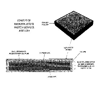
Brief Description of the Drawings
In the drawings, which form part of this specification,
Figure 1 illustrates the concept of the microstructure photomultiplier
assembly;
Figure 2 is a schematic diagram illustrating simulation of electron
trajectories through micro-
structure boards.
Description of Preferred Embodiment
We propose to utilize circuit boards with small channels through them, similar
to the basic
component used by a GEM. However, we propose to deposit an additional layer of
secondary
electron emissive material on the conductive layer, among the holes, to form
what is termed a
multistructured board (MSB). This secondary emissive material can be a
suitable alkali-based
compound or a more robust compound that can be handled under non-vacuum
conditions (e.g.
5
CA 02684811 2009-11-06
see B.N. Laprade, R. Prunier and R. Farr, Poster paper 1340-17P, The
Pittsburgh Conference
2005). This emissive material is only needed on one side of the board (the
side facing the
photocathode). The MPA is conceived to operate in a vacuum, like a
conventional PMT. By
applying a voltage across the board and maintaining a voltage between the
photocathode and the
front face of the MSB, photoelectrons from the photocathode will be drawn
towards the board
surface and be increased in energy by the electric field inside the channel.
These higher energy
electrons will strike the emissive layer of a second MSB, producing additional
secondary
electrons. These low-energy secondary electrons, in turn, will be drawn into
the channel of the
second board where they will be further accelerated by the electric field and
so on, similar to the
electron amplification process in a PMT. Unlike the GEM PMT, no electron-ion
pairs are
produced in the channel since there is no gas. However, the electrons will
emerge from the
channels of the MSB with additional energy provided by the electric field
generated by the
voltage across the board. This energy gain is similar to that between adjacent
dynodes in the
convention PMT. Thus, the channels of the MSB serve to increase the energy of
the electrons
that are entering the channel - similar to the electric field between dynodes.
When these
electrons strike the secondary emissive layer of the next board, they will
produce additional
secondary electrons - in similarity with the function of the next dynode.
Thus, by using an array
of MSBs all operated with a voltage difference between each board, electron
amplification is
achieved in a manner similar to a series of dynodes. Many layers of MSBs can
be used to get a
large enough electron signal. A board without channels can serve as the anode.
The signal from
the anode can exit from the MPA and be ready for processing by conventional
electronics -
identical to the way a PMT is used.
Recent advances in circuit boards technology make the MPA a viable, practical,
timely product.
The desired use of alkali metal-based photocathodes (for high quantum
efficiency in the visible
spectral region) requires operation in a high vacuum environment. Most
traditional circuit
boards are made on a pliable plastic substrate (e.g. woven glass and epoxy).
While such boards
have been shown to be usable under high vacuum conditions if properly "baked"
at elevated
temperatures (R. Rouki, L. Westerberg, and the CHICSi development group,
Physica Scripta
T104 107 - 108 (2003)), little work has been done in assessing the long-term
outgassing of such
boards that are based on plastic substrates. However, in recent years, circuit
boards based on a
6
CA 02684811 2009-11-06
ceramic substrate have become readily available and have been produced in
large scale for
research (e.g. Adamyan F., Avanesyan H., Asatryan M., Chatrchyan S., Hagopian
V.,
Harutunyan B., Haykazyan M., Hovsepyan A., Sirunyan A. and Slinkareva L.,
(Nucl. Inst. Meth.
A 551 (2005) 285-289) and by many commercial suppliers. Such circuit boards
have gained the
reputation of being easy to work with and can handle heating by electronic
component well. For
our application, ceramic-based circuit boards are ideal for high-vacuum
operation. Thus, the
combination of MSBs based on a ceramic substrate, and a photocathode, such as
an alkali-metal
photocathode, operated inside a chamber under high vacuum makes the MPA a
sound, practical
device for detection of weak light signals from any large area (e.g. > 4" x
4") scintillator,
commonly used for detection of radiation.
Of course, the great advantage of the MPA is that the MSB can have many fine
channels down to
about 50 m diameter range. Thus, similar to a GEM or a MCP, this fine
collection of miniature
amplifiers can be used for ultra-fine imaging applications if desired. For
such an application, it
is only necessary to segment the anode into isolated copper "islands", each
covering one or more
channels. By using anode pad read-out technology, spatial resolution in the
tens of microns
range can easily be achieved. Such readouts have already been developed for
the GEM (e.g.,
Kaminski J., Kappler S., Leidermann B., Muller T. and Ronan M., IEEE Trans.
Nucl. Sci. 52
(2005) 2900-2906.) and are commercially available. Such readouts can be
readily applied to the
MPA for imaging applications. Such applications are commonly found in medical
imaging
where high definition is extremely desirable.
While the MPA can be manufactured in a variety of sizes and shapes to suit a
desired
application, we propose a particular embodiment which is appropriate for use
in wide area (e.g.
Im x lm) radiation imaging, of current interest in homeland security
applications. Currently, the
detectors used for x-ray or neutron imaging of vehicles and cargo containers
are in the form of a
thin vertical array. The interrogating beam is a line beam to match the
detector array and the
cargo is moved pass the interrogation beam and the vertical line image of the
cargo is captured
by the detector array. The 2-dimensional image of the entire cargo is created
by the collection of
such vertical images. The vertical detector array itself contains many
individual radiation
detectors. Often, scintillators are used and they all require PMTs or a solid
state equivalent.
7
CA 02684811 2009-11-06
The use of large area detectors (instead of a vertical line detector) would
increase the efficiency
of the imaging process - similar to the use of an area detector in
conventional chest x-rays.
Unfortunately, the use of a large area detector based on current technology
would increase the
cost of the detector system enormously - primarily because of the large
increase in the number of
PMTs (or solid state equivalent) required.
The proposed embodiment of the MPA lowers the high cost for a large area
detector
considerably. We propose a MPA design based on a 12" x 12"x 2" module (to
compared to a 12"
PMT or by tiling of many smaller PMTs). Such a module provides a reasonable
choice for tiling
of larger areas (e.g. lm x lm) while providing flexibility for various, large,
geometric detector
designs.
The proposed MPA module would be in the form of a square, preferably stainless
steel, box 12"
x 12"x 2" high, having a thick (-1/4") glass plate on the front face as shown
in Fig. 1. This
sealed enclosure must be strong enough to withstand atmospheric pressure with
a high vacuum
within. The inside of the glass surface would be coated with a conventional S-
11 or similar
photocathode, approximately 0.25 m thick. Three to more than a dozen MSBs of
thickness 1
mm with, say, 0.3mm diameter channels at 0.7mm pitch, each isolated from one
another by
ceramic insulator stand-offs (2mm thick), are placed adjacent to the
photocathode (-2mm
distance). Each of the circuit boards (with ceramic substrate) have electrical
connections to both
sides of the board and these electrical leads allow the application of high
voltage outside the
MPA, similar to the pins that allow high voltage to be applied to the dynodes
of a PMT. Thus
each circuit board has 1 pair of external electrical connections. An anode
plate consisting of a
circuit board without channels can be used to provide signal output. If
imaging is not required, a
single pin to the outside of the MPA from the anode can be used for signal
output. If imaging is
required, the anode can be segmented into as small areas as desired and these
could take the form
of a pad matrix (in PCB) that can be read out using a variety of pad readout
technology such as
charge division or commercial multi-channel readout Electronics for Nuclear
Applications. The
MPA is operated under high vacuum. In concept, the MPA can be used whenever
there is a need
for a large PMT, or in place of tiling large area scintillators with a number
of smaller PMT (as is
commonly done in "gamma cameras" used in medical diagnosis). Its operation
requires a supply
8
CA 02684811 2009-11-06
of high voltage (as for PMTs) and the use of preamplifiers and
analogue/digital data processing
electronics (as for PMTS). In fact, the MPA when used for imaging applications
can be regarded
as a much larger version of a commonly-available multi-anode PMT or a MCP,
often used
whenever there is a need to have many independent electron amplifiers within a
single electronic
device.
Simulations have been done to show that the MPA can provide electron
amplification similar to
a conventional (or Multi-anode) PMT. These were done using SIMION, a standard
code used for
the design of electro-optical systems. Fig. 2 shows a schematic diagram of the
simulations. Low-
energy photoelectrons were assumed to be emitted over 27E steradians from the
photocathode.
These electrons strike the front face of the first microstructure board. The
voltages on the both
sides of this board were adjusted to attain an increase in the production of
secondary electrons on
the front surface of this board and to guide these low-energy secondary
electrons through the
channels of the board, where they gain additional energy due to the electric
field in the channel.
This process is repeated for the following boards. Thus, in each board after
the first, there is a net
gain (^) of electrons per board. In these simulations, by using S-11 coatings
on the
microstructure board, we attained a net gain of approximately 2.5 times per
board. Thus, a series
of n microstructure boards will provide an overall gain of (^)". For 10
stages, a typical gain of a
104 can be attained. This is sufficient for many radiation sensors of interest
to radiation detection
and spectroscopy. Of course, optimizing the design of the MSB can lead to
higher gains per stage
and the use of more stages will lead to higher overall gain. By using pad
readout, high quality
imaging of objects of interest to medical physics or homeland security can be
attained. By using
a single anode plate, the MPA functions essentially as a large-area PMT.
9