Note: Descriptions are shown in the official language in which they were submitted.
,
= CA 02684917 2009-10-29
WO 2008/135637
PCT/F12008/050244
POWER SUPPLIES FOR RF POWER AMPLIFIER
FIELD OF THE INVENTION
The present invention relates to switched-mode power supplies, and
more specifically to switched-mode power supplies and their control methods
for radio frequency (RF) power amplifiers in battery-powered wireless transmit-
ter devices.
BACKGROUND OF THE INVENTION
Energy-efficient radio frequency (RF) power amplifiers (PA) are
critical components in mobile, battery-operated wireless communication de-
vices, e.g. mobile phones, personal digital assistants (PDA), etc., because
they
determine a significant portion of the total power consumption of such
devices.
Batteries with low supply voltage, typically about 3V, are employed in the
port-
able devices. It has been possible to design a PA for the 3V battery voltage
even if the efficiency already has dropped a bit. In order to get high
efficiency
from a PA, a switching-mode power supply (SMPS), often referred to as a
Boost converter or a step-up converter is needed to up-convert the battery
voltage to a value higher than the maximum battery voltage. With this ap-
proach, the needed output transmission power can be easily obtained from the
PA, but the efficiency for small transmission power levels is poor. To improve
efficiency also at the small transmission power levels, the supply voltage of
the
PA must be lowered. This is not possible with a Boost-type power supply but
another type of switching-mode power supply (often referred to as a Buck con-
verter, or a step-down converter) is provided to down-convert the raised bat-
tery voltage to the level needed for actual transmission power level. If the
two
converters are cascaded, the efficiency at low transmission power levels suf-
fers from the cascaded converters and the high voltage between them.
Some RF PA applications with a switching-mode power supply
(SMPS) use a dynamic biasing PA, such as the envelope elimination and res-
toration (EER) technique, to achieve high-efficiency, linear power
amplification.
In the EER, the phase and envelope information are extracted from the original
modulated signal. A constant envelope signal containing the phase information
is amplified using an RF PA. Since the phase information has a constant enve-
lope, the PA can be highly overdriven to achieve high efficiency. The envelope
information is fed into the power supply circuit to modulate the supply
voltage
of the RF PA (e.g. drain or collector voltage) and thereby superimpose the en-
' CA 02684917 2009-10-29
WO 2008/135637
PCT/F12008/050244
2
velope variation. By changing the supply voltage, the output waveform will be
shaped and the overall amplification can be linear. There are also simplified
versions of the EER, such as the envelope tracking (ET) technique. In the ET
technique, the input signal to the RF amplifier contains both the phase
informa-
tion and the amplitude information, and only the envelope information is ex-
tracted for the switching power supply. The RF PA is operated in the linear re-
gion and its supply voltage is changed according to the extracted envelope
information. The supply voltage is varied with sufficient headroom to minimize
distortion. Examples of transmitter architectures employing EER technique are
disclosed in US 6,256,482 and W02006/085,177. A still further version is
power-level tracking (PT) in which a switching-mode power supply tracks only
the slow-varying average power level, instead of the fast-varying envelope,
and modulates the drain or collector voltage of a linear PA.
So-called Buck-Boost converters also exist. An example of a Buck-
Boost converter is disclosed in US Patent 6,348,781. The Buck-Boost convert-
ers are designed to change mode from Buck to Boost automatically to provide
a supply voltage that ensures good efficiency of an RF PA at any specific
transmission power level. No cascading is needed. However, in applications
that use the envelope elimination and restoration (EER) technique, a very
tightly controlled frequency and group delay response is needed. With a Buck-
Boost switching-mode power supply, the output voltage range where the mode
changes is quite critical, and distortion occurs. Also, in the Boost mode of
op-
eration it is difficult to keep the response unaffected. Buck-Boost converters
are good choices for power level tracking where the frequency and group delay
requirements are loose.
The problems regarding efficiency are becoming more significant
with the battery technology, e.g. lithium battery technology, lowering the cut
of
voltage from the present range, e.g. 3V, to about 2.5V or lower. As a conse-
quence, a transmission (TX) power amplifier becomes very inefficient and
variation in its performance increases, if it is designed for 2.3V supply
voltage,
for example.
A SUMMARY OF THE INVENTION
Some aspects of the present invention are disclosed in the attached
independent claims. Various embodiments of the invention are disclosed in the
dependent claims.
CA 02684917 2013-10-28
3
According to an aspect there is provided a method comprising:
measuring a battery voltage inputted to a cascade connection of a
boost-type switched-mode power supply and a buck-type switched-mode
power supply providing a supply voltage to a radio frequency power amplifier,
wherein at least one of the buck-type switched-mode power supply and the boost-
type switched-mode power supply comprises at least two section modes having at
least two parallel switches such that in a first one of the section modes both
of the
two parallel switches are switched on and off at a switching frequency to
provide a
maximum load current to the radio frequency power amplifier, and in a second
one
of the section modes a first one of the parallel switches is switched on and
off at
the switching frequency;
comparing the measured battery voltage with a threshold
corresponding to an input supply voltage which is needed for the buck-type
switched-mode power supply;
bypassing the boost-type switched-mode power supply and coupling
the battery voltage directly to the buck-type switched-mode power supply, if
the measured battery voltage exceeds a needed input supply voltage;
controlling the boost-type switched-mode power supply to raise the
battery voltage to at least the needed input supply voltage, if the measured
battery voltage is below the needed input supply voltage; and
controlling the buck-type switched-mode power supply to operate in one
of the at least two section modes according to one or more of the following: a
mode of operation of the power amplifier, a frequency band of the power
amplifier, a modulation method, and a transmission power of the power
amplifier.
According to another aspect there is provided a non-transitory computer
readable medium embodying a computer program, the computer program
comprising program code for controlling a processor to execute a routine
comprising:
measuring a battery voltage inputted to a cascade connection of a
boost-type switched-mode power supply and a buck-type switched-mode
power supply providing a supply voltage to a radio frequency power amplifier,
wherein at least one of the buck-type switched-mode power supply and the boost-
type switched-mode power supply comprises at least two section modes having at
least two parallel switches such that in a first one of the section modes both
of the
Iwo parallel switches are switched on and off at a switching frequency to
provide a
maximum load current to the radio frequency power amplifier, and in a second
one
= CA 02684917 2013-02-08
4
of the section modes a first one of the parallel switches is switched on and
off at
the switching frequency;
comparing the measured battery voltage with a threshold corresponding
to an input supply voltage which is needed for the buck-type switched-mode
power supply;
bypassing the boost-type switched-mode power supply and coupling the
battery voltage directly to the buck-type switched-mode power supply, if the
measured battery voltage exceeds a needed input supply voltage;
controlling the boost-type switched-mode power supply to raise the
battery voltage to at least the needed input supply voltage, if the measured
battery voltage is below the needed input supply voltage; and
controlling the buck-type switched-mode power supply to operate in one of
the at least two section modes according to one or more of the following: a
mode of operation of the power amplifier, a frequency band of the power
amplifier, a modulation method, and a transmission power of the power
nmplifier.
According to yet another aspect there is provided an apparatus
comprising:
at least one radio frequency power amplifier;
a boost-type switched-mode power supply having an input for a battery
voltage from a battery;
a buck-type switched-mode power supply connected in cascade with
the boost-type switched-mode power supply and having a supply voltage output
for the radio frequency power amplifier;
a bypass switch controllable to bypass the boost-type switched-mode
power supply and to couple the battery voltage directly to the buck-type
switched-mode power supply, if the battery voltage exceeds a threshold
corresponding to an input supply voltage which is needed for the buck-type
.
switched-mode power supply;
the boost-type switched-mode power supply being controllable to raise
the battery voltage to at least a needed input supply voltage, if the battery
voltage is below the threshold; and
wherein at least one of the buck-type switched-mode power supply and
the boost-type switched-mode power supply comprises at least two section
modes having at least two parallel switches such that in a first one of the
section modes both of the two parallel switches are switched on and off at a
switching frequency to provide a maximum load current to the at least one
CA 02684917 2013-02-08
4a
radio frequency power amplifier, and in a second one of the section modes a
first one of the parallel switches is switched on and off at the switching
frequency,
the buck-type switched-mode power supply comprising the at least two
section modes selectable according to one or more of the following: a mode of
operation of the power amplifier, a frequency band of the power amplifier, a
modulation method, and a transmission power of the power amplifier.
According to still yet another aspect there is provided a method
comprising:
providing a cascade connection of a boost-type switched-mode power
supply and a buck-type switched-mode power supply to provide a supply voltage
= to a radio frequency power amplifier from a battery voltage, wherein at
least one
of the buck-type switched-mode power supply and the boost-type switched-mode
power supply comprises at least two section modes having at least two parallel
switches such that in a first one of the section modes both of the two
parallel
switches are switched on and off at a switching frequency to provide a maximum
load
current to the radio frequency power amplifier, and in a second one of the
section
modes a first one of the parallel switches is switched on and off at the
switching
frequency;
controlling the boost-type switched-mode power supply to raise the
battery voltage to at least an input supply voltage which is needed for the
buck-
type switched-mode power supply; and
controlling the buck-type switched-mode power supply to operate in one
of the at least two section modes according to one or more of the following: a
mode of operation of the power amplifier, a frequency band of the power
amplifier, a modulation method, and a transmission power of the power
amplifier.
According to still yet another aspect there is provided a method
comprising:
providing a cascade connection of a boost-type switched-mode power
supply and a buck-type switched-mode power supply to provide a supply voltage
to a radio frequency power amplifier from a battery voltage, wherein at least
one of the buck-type switched-mode power supply and the boost-type
switched-mode power supply comprises at least two section modes having at
least two parallel switches such that in a first one of the section modes both
of
the two parallel switches are switched on and off at a switching frequency to
provide a maximum load current to the radio frequency power amplifier, and in
CA 02684917 2013-10-28
- = .
4b
a second one of the section modes a first one of the parallel switches is
switched on and off at the switching frequency;
controlling the boost-type switched-mode power supply to raise the
battery voltage to at least an input supply voltage which is needed for the
buck-
type switched-mode power supply; and
controlling the buck-type switched-mode power supply to operate at a
higher switching frequency, when the power amplifier operates in an envelope
elimination and restoration mode or in an envelope tracking mode, and to
operate at a lower switching frequency, when the power amplifier operates in a
linear mode.
According to still yet another aspect there is provided a non-transitory
computer readable medium embodying a computer program, the computer
program comprising program code for controlling a processor to execute a
routine comprising:
providing a cascade connection of a boost-type switched-mode power
supply and a buck-type switched-mode power supply to provide a supply voltage
to a radio frequency power amplifier from a battery voltage, wherein at least
one
of the buck-type switched-mode power supply and the boost-type switched-mode
power supply comprises at least two section modes having at least two parallel
switches such that in a first one of the section modes both of the two
parallel
switches are switched on and off at a switching frequency to provide a maximum
load current to the radio frequency power amplifier, and in a second one of
the
section modes a first one of the parallel switches is switched on and off at
the
switching frequency;
controlling the boost-type switched-mode power supply to raise the
battery voltage to at least an input supply voltage which is needed for the
buck-
type switched-mode power supply; and
controlling the buck-type switched-mode power supply to operate in one
of the at least two section modes according to one or more of the following: a
mode of operation of the power amplifier, a frequency band of the power
amplifier, a modulation method, and a transmission power of the power
amplifier.
According to still yet another aspect there is provided a controller
comprising:
means for measuring a battery voltage inputted to a cascade connection of
a boost-type switched-mode power supply and a buck-type switched-mode power
supply providing a supply voltage to a radio frequency power amplifier,
wherein at
CA 02684917 2013-10-28
. =
4c
least one of the buck-type switched-mode power supply and the boost-type
switched-mode power supply comprises at least two section modes having at
least
two parallel switches such that in a first one of the section modes both of
the two
parallel switches are switched on and off at a switching frequency to provide
a
maximum load current to the radio frequency power amplifier, and in a second
one
of the section modes a first one of the parallel switches is switched on and
off at
the switching frequency;
means for comparing the measured battery voltage with a threshold
corresponding to an input supply voltage which is needed for the buck-type
switched-mode power supply;
means for bypassing the boost-type switched-mode power supply and
coupling the battery voltage directly to the buck-type switched-mode power
supply, if the measured battery voltage exceeds the input supply voltage;
means for controlling the boost-type switched-mode power supply to
raise the battery voltage to at least the input supply voltage, if the
measured
battery voltage is below the input supply voltage; and
means for controlling the buck-type switched-mode power supply to
operate in one of the at least two section modes according to one or more of
the following: a mode of operation of the power amplifier, a frequency band of
the power amplifier, a modulation method, and a transmission power of the
power amplifier.
According to still yet another aspect there is provided a non-transitory
computer readable medium embodying a computer program, the computer
program comprising program code for controlling a processor to execute a
routine comprising:
providing a cascade connection of a boost-type switched-mode power
supply and a buck-type switched-mode power supply to provide a supply voltage
to a radio frequency power amplifier from a battery voltage, wherein at least
one of the buck-type switched-mode power supply and the boost-type
switched-mode power supply comprises at least two section modes having at
least two parallel switches such that in a first one of the section modes both
of
the two parallel switches are switched on and off at a switching frequency to
provide a maximum load current to the radio frequency power amplifier, and in
a second one of the section modes a first one of the parallel switches is
switched on and off at the switching frequency;
CA 02684917 2013-02-08
4d
controlling the boost-type switched-mode power supply to raise the
battery voltage to at least an input supply voltage which is needed for the
buck-
type switched-mode power supply; and
controlling the buck-type switched-mode power supply to operate at a
higher switching frequency, when the power amplifier operates in an envelope
elimination and restoration mode or in an envelope tracking mode, and to
operate
at a lower switching frequency, when the power amplifier operates in a linear
mode.
According to still yet another aspect there is provided a controller
comprising:
means for providing a cascade connection of a boost-type switched-
mode power supply and a buck-type switched-mode power supply to provide a
supply voltage to a radio frequency power amplifier from a battery voltage,
wherein at least one of the buck-type switched-mode power supply and the
boost-type switched-mode power supply comprises at least two section modes
having at least two parallel switches such that in a first one of the section
modes both of the two parallel switches are switched on and off at a switching
frequency to provide a maximum load current to the radio frequency power
amplifier, and in a second one of the section modes a first one of the
parallel
switches is switched on and off at the switching frequency;
means for controlling the boost-type switched-mode power supply to raise
the battery voltage to at least an input supply voltage which is needed for
the
buck-type switched-mode power supply; and
means for controlling the buck-type switched-mode power supply to
operate at a higher switching frequency, when the power amplifier operates in
an envelope elimination and restoration mode or in an envelope tracking mode,
and to operate at a lower switching frequency, when the power amplifier
operates in a linear mode.
CA 02684917 2009-10-29
WO 2008/135637 PCT/F12008/050244
BRIEF DESCRIPTION OF THE DRAWINGS
In the following the invention will be described in greater detail by
means of exemplary embodiments with reference to the attached drawings, in
which
5 Figure 1 is a block diagram illustrating an example of a transmitter
according to an embodiment of the present invention;
Figure 2 is a schematic diagram illustrating an example of a boost-
type switched-mode power supply according an embodiment of the invention;
Figure 3 is a schematic diagram illustrating an example of a buck-
type switched-mode power supply according an embodiment of the invention;
Figure 4 is a flow diagram illustrating an example of a control algo-
rithm for controlling a boost-type switched-mode power supply in accordance
with an embodiment of the invention; and
Figure 5 is a flow diagram illustrating an example of a control algo-
rithm for controlling a buck-type switched-mode power supply in accordance
with an embodiment of the invention.
DETAILED DESCRIPTION OF THE INVENTION
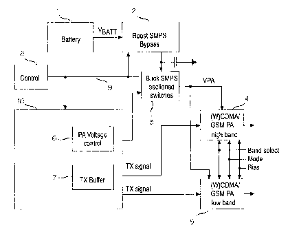
Referring to Figure 1, a block diagram of an exemplary RF transmit-
ter (TX) circuitry is shown in which a supply voltage is provided from a
battery
1 to power amplifiers (PA) 4, 5 through cascaded Boost and Buck switched-
mode power supplies (SMPS) 2, 3.
A battery 1 provides a battery voltage Vbatt to a Boost-type switched
mode power supply 2 according to an embodiment of the invention. The bat-
tery may be any type of battery suitable for portable devices, such as a
lithium
cell battery or a nickel cadmium battery. The battery voltage Vbatt may have
any low voltage value depending on the application and the battery technology
selected. A typical battery voltage may be about 3 Volts or lower, or even 2.5
Volts or lower.
The Boost switched-mode power supply 2 up-converts from the bat-
tery voltage Vbatt a supply voltage V2 with a raised voltage level to a Buck-
type
switched-mode power supply 3. The Boost switched-mode power supply may
also include a bypass function that bypasses the battery voltage Vbatt to form
the supply voltage V2 to the Buck-type switched-mode power supply 3 without
boosting. The Boost switched-mode power supply 2 may also include sec-
tioned transistor switches as will be described below. A boost condensator Cl
CA 02684917 2009-10-29
WO 2008/135637 PCT/F12008/050244
6
filters high-frequency interference from the boosted voltage V2.
The Buck-type switched-mode power supply 3 down-converts from
the supply voltage V2 a supply voltage V1 for the RF power amplifiers (PA) 4
and 5. The Buck-type switched-mode power supply 3 may also include sec-
tioned transistor switches as will be described below. The Buck SMPS 3 may
provide a biasing control for the PAs 4 and 5 by modulating their supply volt-
age V1 connected to the collectors of the PAs 4 and 5. To that purpose, a PA
supply voltage control unit 6 in the transmitter circuitry may provide a PA
volt-
age control signal to the Buck SMPS 3. For example, for the envelope elimina-
tion and restoration (EER) technique, envelope tracking (ET) technique, or
power-level tracking (PT), the PA voltage control signal from the control unit
6
may represent envelope information derived from the modulated signal, so that
the voltage control signal causes the Buck SMPS 3 to modulate the supply
voltage V1. In an embodiment, the Buck SMPS 3 may be controlled directly
with duty cycle information (command) when the Buck SMPS 3 has an internal
duty cycle generator. In another embodiment, a control signal required with
the
wanted duty cycle is sent to the input of a switch driver in the Buck SMPS 3.
Nowadays, mobile communication devices are often multimode and
multiband devices supporting two or more frequency bands and modulation
formats (for example, GSM, EDGE, COMA, WCDMA). It is logical to use as
few RF power amplifiers as possible but typically at least a low frequency
band
(such as 900 MHz band for GSM/EDGE/WCDMA) and a high frequency band
(such as 1800/1900 MHz band for GSM/EDGE/WCDMA) use different RF
power amplifiers even if the amplifiers were implemented inside the same RF
module and even on the same chip. In the embodiment shown in Figure 1,
there are two RF power amplifiers (PAs), the RF PA 4 for a high frequency
band (e.g. 1800/1900 MHz) of one or more systems (such as GSM, COMA,
WCDMA), and the RF PA 5 for a low frequency band (such as 900 MHz) of
one or more systems (such as GSM, CDMA, WCDMA). However, the present
invention is not intended to be restricted to this number of power amplifiers
but
all bands may be implemented by means of one power amplifier, or there may
be more power amplifiers with dedicated frequency bands. It should also be
appreciated that the mobile communication systems and frequency bands
mentioned are only examples, and the present invention can be applied to any
mobile communication systems and frequency bands.
CA 02684917 2009-10-29
WO 2008/135637 PCT/F12008/050244
7
A power amplifier may have several different modes of operation,
for example a linear mode for the envelope tracking (ET) and power tracking
(PT) operation, and a compressed mode for the EER operation. The needed
transmission output powers are different for different cellular systems and
fre-
quency bands. For instance, for the GSM900 system the needed maximum
output power may be 2W or 33dBm, for the GSM1800 system the needed
maximum output power may be 1W (30dBm), and for WCDMA on both bands
the needed maximum output power may 24 dBnn on average. If the output
matching of RF PAs is fixed (could also be switchable), the RF PAs are usually
designed so that the maximum wanted power is obtained with a certain collec-
tor voltage, for example 4.5V. When lower power is needed, the collector volt-
age can be reduced and this may be achieved with a buck converter. Also, the
needed amount of current with maximum output power is less for the high fre-
quency band (1W versus 2W in the example above). Because the same
switched-mode power supplies feed the PAs operating in different frequency
bands and thereby with different transmission powers, the SMPSs need to be
designed for the heaviest load (in the example above, to feed the GSM900
band requires a maximum power of 2W). When another PA or another modula-
tion or a lower output power is used, the efficiency of the SMPSs is not opti-
mum.
According to embodiments of the invention, the Buck-type SMPS or
the Boost-type SMPS or both may be configured to be sectioned SMPSs. In
other words, the transistor switches may be implemented with parallel transis-
tors, instead of single transistors, so that it is possible to selectively use
some
or all of the parallel transistors according to the load at each specific
moment
and thus reduce the capacitive switching losses.
An example schematic diagram of a sectioned bypass Boost
switched-mode power supply (SMPS) according to an embodiment of the in-
vention is shown in Figure 2. The battery voltage VBATT from the battery 1 at
an
input node A is coupled to one end of a boost inductor Lboost, the second end
of
which is coupled to a circuit node B. A voltage meter 26 may be provided to
measure the battery voltage and to forward the measurement result to a con-
trol unit 8 via a control bus/line 9. Parallel high-side switches BHSW1 and
BHSW2 are coupled between the node B and an output node C, and parallel
low-side switches BLSW1 and BLSW2 are connected between the node B and
a ground potential, for example. A bypass switch BPSW1 may further be con-
CA 02684917 2009-10-29
WO 2008/135637 PCT/F12008/050244
8
nected between the input node A and the output node C to selectively bypass
the boost inductor Lboost and the high-side switches BHSW1 and BHSW2, and
thereby to couple the battery voltage VBATT directly to the Buck SMPS 3. The
control inputs of switches BHSW1, BHSW2, BLSW1, BLSW2 and BPSW1 are
controlled by respective control signals from a switch driver 21. Depending on
the Boost section mode selected according to a boost section select control
input, the switch driver 21 turns selected boost switches BHSW1, BHSW2,
BLSW1 and BLSW2 ON (conductive) and OFF (non-conductive) under the
control of a pulse width modulated (PWM) signal having a predetermined
switching frequency. The switching frequency is generated by a switching fre-
quency generator, such as a sawtooth waveform generator 22 in Figure 2. The
switching frequency may be set by a boost frequency control signal. The
sawtooth waveform from the generator 22 may be applied to a first input of a
comparator 23, such as a Smith trigger. The voltage V2 at the output node C is
coupled via a feedback network 24 to a first input of a further comparator 25.
A
boost voltage control signal that determines the desired boost voltage V2 is
applied to a second input of the comparator 25. An output voltage of the com-
parator 25 is thus proportional to the difference between the desired boost
voltage and the actual output voltage V2, and it is applied to a second input
of
a comparator 23. The state of the output from the comparator 23 changes
each time the level of the sawtooth waveform exceeds the output voltage from
the comparator 25. Thereby a PWM signal is provided whose frequency is set
by the frequency of the sawtooth signal and whose duty cycle is set by the dif-
ference between the desired and actual boost voltage V2. If the bypass switch
BPSW1 is turned on, and the Boost SPMS is bypassed, all boost switches
BHSW1, BHSW2, BLSW1 and BLSW2 may be turned off, or the high side
switches BHSW1 and BHSW2 may be kept on in order to decrease the total
resistance from battery to output because the current flows through the high
side switches and the bypass switch. The latter arrangement allows to size the
bypass switch smaller and thereby saves chip area in integrated implementa-
tions. The boost section select, the boost frequency control, and the boost
voltage control may be obtained through the control bus/line 9 from a transmit-
ter control unit 8. It should be appreciated that this is only one example of
many possible ways to implement the switch drive and control.
In an embodiment of the invention, the Boost SMPS 2 may be con-
figured to have three section modes. In the first section mode, all switches
CA 02684917 2009-10-29
WO 2008/135637 PCT/F12008/050244
9
BHSW1, BHSW2, BLSW1 and BLSW2 are selected. In the second section
mode, the switches BHSW1 and BLSW1 are selected. In the third section
mode, the switches BHSW2 and BLSW2 are selected. One example of possi-
ble sizing of switches BHSW1, BHSW2, BLSW1 and BLSW2, when field effect
transistors (FETs) are used, could be as follows. If the needed FET size for
maximum current is W=21 mm (wherein W is a channel width whose value
depends on a needed switch resistance), this maximum size could be split be-
tween two parallel FETs, so that a first FET (e.g. BHSW1 and BLSW1) has a
size W=14mm and a second FET (e.g. BHSW2 and BLSW2) has a size
W=7mm. Thus, in the first section mode, when both parallel switches BHSW1
and BHSW2, or BLSW1 and BLSW2, respectively, are activated, the total ef-
fective width of the parallel switches is 21mm. In the second section mode,
when only the bigger switch, BHSW1 and BLSW1, is selected in each pair of
parallel switches, the active size is 14mm. Similarly, in the third section
mode,
when only the smaller switch, BHSW2 and BLSW2, is selected in each pair of
parallel switches, the active size is 7mm. As a result, the driving losses are
reduced to two 3rds in the second section mode and to one 3rd in the third sec-
tion mode in relation to the first section mode, i.e. the full load. It should
be ap-
preciated that the invention is not intended to be restricted to the sizing
pre-
sented in the above example but the sizing can be freely chosen for each ap-
plication, depending on the number of parallel switches, the number of desired
section modes, the type and number of different loads, for example.
It should also be appreciated that the number of different section
modes can be freely chosen for each application. In an embodiment of the in-
vention, there is no sectioning of the boost switches at all, and bypass
switch-
ing is implemented. In an embodiment of the invention, the Boost SMPS 2
shown in Figure 2 may be configured to have two section modes. With the ex-
emplary sizing described above, in the first section mode, all switches BHSW1,
BHSW2, BLSW1 and BLSW2 may be selected, and in the second section
mode, the switches BHSW1 and BLSW1 or the switches BHSW2 and BLSW2
may be selected. As another example, if the switches BHSW1 and BLSW1 are
sized for a full load (e.g. W=21mm) and the switches BHSW2 and BLSW2 are
sized for a half load (e.g. W=10mm), BHSW1 and BLSW1 may be selected in
the first section mode and BHSW2 and BLSW2 may be selected in the second
section mode. In most applications, two or three section modes provide a suffi-
CA 02684917 2009-10-29
WO 2008/135637 PCT/F12008/050244
cient improvement in the performance in comparison with the complexity and
cost of the additional control.
An example schematic diagram of a sectioned Buck switched-mode
power supply (SMPS) according to an embodiment of the invention is shown in
5 Figure 3. The voltage V2 (i.e. the boosted voltage or the bypassed
battery volt-
age VBATT) from the Boost SMPS 2 is inputted to the Buck SMPS 3 at an input
node D. Parallel high-side switches BUHSW1 and BUHSW2 are coupled be-
tween the node D and a node E, and parallel low-side switches BULSW1 and
BULSW2 are connected between the node E and a ground potential, for ex-
10 ample. A buck inductor Lbuck is connected between the node E and the
output
node F. A buck capacitor C2 is connected between the node F and the ground
potential. The control inputs of switches BUHSW1, BUHSW2, BULSW1 and
BULSW2 are controlled by respective control signals from a switch driver 31.
Depending on the Buck section mode selected according to a buck section
select control input, the switch driver 31 turns selected ones of the boost
switches BUHSW1, BUHSW2, BULSW1 and BULSW2 ON (conductive) and
OFF (non-conductive) under the control of a pulse width modulated (PWM)
signal having a predetermined switching frequency. The switching frequency is
generated by a switching frequency generator, such as a sawtooth waveform
generator 32. The switching frequency may be set by a buck frequency control
signal. The sawtooth waveform from the generator 32 may be applied to a first
input of a comparator 33, such as a Smith trigger. The voltage V1 at the
output
node F is coupled via a feedback network 34 to a first input of a further com-
parator 35. An envelope or voltage control signal from the PA voltage control
circuit 6 may be applied to a second input of the comparator 35. An output
voltage of the comparator 35 is thus proportional to the difference between
the
envelope information (representing the desired buck voltage) and the actual
output voltage V1, and it is applied to a second input of the comparator 33.
The
state of the output from the comparator 33 changes each time the level of the
sawtooth waveform exceeds the output voltage from the comparator 35.
Thereby a PWM signal is provided whose frequency is set by the frequency of
the sawtooth signal and whose duty cycle is set by the difference between the
desired and actual buck voltage V1. The buck section select and the buck fre-
quency control may be obtained through the control bus/line 9 from a transmit-
ter control unit 8. It should be appreciated that this is only one example of
many possible ways to implement the switch drive and control.
CA 02684917 2009-10-29
WO 2008/135637 PCT/FI2008/050244
11
In an embodiment of the invention, the Buck SMPS 3 may be con-
figured to have three section modes. In the first section mode, all switches
BUHSW1, BUHSW2, BULSW1 and BULSW2 are selected. In the second sec-
tion mode, the switches BUHSW1 and BULSW1 are selected. In the third sec-
tion mode, the switches BUHSW2 and BULSW2 are selected. One example of
possible sizing of switches BUHSW1, BUHSW2, BULSW1 and BULSW2 is
similar to that described in connection with the Boost SMPS 2 in Figure 2.
However, it should be appreciated that the invention is not intended to be re-
stricted to the sizing presented in that example but the sizing can be freely
chosen for each application, depending on the number of parallel switches, the
number of desired section modes, the type and number of different loads, for
example.
It should also be appreciated that the number of different section
modes can be freely chosen for each application, in a manner similar to that
described in connection with the Boost SMPS 2 in Figure 2. Thus, in an em-
bodiment of the invention, the Buck SMPS 3 shown in Figure 3 may be config-
ured to have two section modes. With the exemplary sizing described above,
in the first section mode, all switches BUHSW1, BUHSW2, BULSW1 and
BULSW2 may be selected, and in the second section mode, the switches
BUHSW1 and BULSW1 or the switches BUHSW2 and BULSW2 may be se-
lected. As another example, if the switches BUHSW1 and BULSW1 are sized
for a full load (e.g. W=21mm) and the switches BUHSW2 and BULSW2 are
sized for a half load (e.g. W=10mm), BUHSW1 and BULSW1 may be selected
in the first section mode and BUHSW2 and BULSW2 may be selected in the
second section mode. In most applications, two or three section modes provide
a sufficient improvement in the performance in comparison with the complexity
and cost of the additional control.
The frequency control allows changing the switching frequency of
the Boost SMPS 2 and the Buck SMPS 3 for different modes. Some modes,
such as those using EER, ET or PT require relatively high switching frequency
in order to achieve the required accuracy. A high switching frequency de-
creases the efficiency with increasing switching losses (parasitic
capacitances
of a switching stage and its control gates are charged and discharged at the
switching frequency). Therefore, efficiency can be improved by lowering the
switching frequency in the modes where it is possible. In an embodiment of the
invention, the frequency control may also include a dithering mode where the
,
CA 02684917 2009-10-29
WO 2008/135637
PCT/FI2008/050244
12
frequency is changed randomly from cycle to cycle. Dithering spreads the
switching frequency spuriously over a wider band and thus reduces the aver-
age spur power density.
According to embodiments of the invention, the Boost SMPS 2 and
the Buck SMPS 3 in cascade connection are controlled so that high efficiency
is maintained for various loads and transmission power levels. The Boost
SMPS 2 and the Buck SMPS 3 may be controlled based on the mode of op-
eration of the transmitter, such as the actual battery voltage, the needed
output
power, the selected frequency band, the selected RF power amplifier (PA), the
selected modulation method of the transmission signal, and/or the selected PA
voltage control method, such as the envelope elimination and restoration
(EER) technique, the envelope tracking (ET) technique, or the power-level
tracking (PT).
For example, in an embodiment of the invention, because the
switching losses depend directly on the voltage range over which the signal is
swinging, the Boost SMPS 2 may be switched off and put into a bypass mode
when the battery voltage VBATT exceeds by a certain amount the actual needed
collector voltage of a PA, so as to decrease the switching losses and to en-
hance efficiency.
The supply currents taken by a PA may be different for the same
collector voltage depending on the frequency band and mode of operation se-
lected. For example, the highest supply currents are needed for the GSM900
transmission at the maximum power level, and thereby the first section mode
enabling the high currents may be selected in the Boost SMPS 2 and/or Buck
SMPS 3. For WCDMA, for example, the maximum currents and needed volt-
ages are much less. Therefore, with the nominal battery voltage the Boost
SMPS 2 may be bypassed for all WCDMA power levels and/or the second or
third section mode may be selected in the Buck SMPS 3 in order to enhance
efficiency.
As a further example, according to an embodiment of the invention,
if the WCDMA PA collector voltage is controlled according to the power level
(the PT technique), then the switching frequency of Buck SMPS 3 can be re-
duced to decrease the switching losses, because there is no need for fast
changes in voltage and the PA is also less sensitive to the ripple in
collector
voltage when used in the linear mode of operation, such as the PT. On the
other hand, if the GSM PA collector voltage is controlled according to the EER
CA 02684917 2009-10-29
WO 2008/135637 PCT/F12008/050244
13
or the ET technique, higher accuracy and a higher switching frequency of the
Buck SMPS 3 is required.
In the following, examples of the operation of the transmitter and the
control of the Boost and Buck SMPSs according to embodiments of the inven-
tion are described.
Control of the transmitter may be provided from a transmitter control
unit 8 that may be implemented by a control unit controlling the whole opera-
tion of a wireless communication device, such a cellular telephone. The
control
unit 8 may select a mode of operation for a multimode multiband wireless
communication device and configure the RF power amplifiers 4 and 5 as well
as the transmitter front stages 10 accordingly.
The switches BHSW1, BHSW2, BLSW1 and BLSW2 of the Boost
SMPS 2 as well as the switches BUHSW1, BUHSW2, BULSW1 and BULSW2
of the Buck SMPS 3 are typically enabled only during the transmission of radio
bursts, and disabled otherwise. Consequently, the RE PAs 4 and 5 may be
energized only during the radio bursts.
When a transmitter (TX) is needed to start, the first step is to start
the Boost SMPS 2. Then the Buck SMPS 3 is started and needed control volt-
age from PA voltage control unit 6 is set. The PA voltage control unit 6 may
include a digital-to-analog converter (DAC) for converting digital voltage
control
values into an analog signal. For example, the digital voltage control value
that
is written to the DAC may range from 0 to 2048, whereby the value 2048 may
give an output voltage of 4.7 V from the Buck SMPS 3. Alternatively, it is
also
possible to control the buck SMPS 3 directly with duty cycle information (corn-
mand), if the buck SMPS 3 has an internal duty cycle generator, or send an
input signal required with the wanted duty cycle (e.g. a signal similar to the
PWM signal in Figure 3) to the input of switch driver 31.
The control of the Boost and Buck SMPSs according to a battery
voltage VBATT, the selected transmission power level, the selected PA (the se-
lected frequency band) and/or the selected mode may be as described in the
following with reference to Figures 4 and 5.
Control of the Boost SMPS 2
Referring to Figure 4, it is first checked whether the transmitter op-
erates in the EER or ET mode in step 41. If the transmitter operates in the
EER
or ET mode, the boost switching frequency is set to a frequency 1 (e.g. 8 MHz)
,
CA 02684917 2009-10-29
WO 2008/135637
PCT/FI2008/050244
14
by means of the boost frequency control signal applied to the generator 22,
step 43. In an embodiment of the invention, different buck switching frequen-
cies 1 and 1' may be set for EER and ET, respectively. A lower frequency 1'
may be used in the ET mode because it is more linear than EER. However,
fast envelope tracking is easier achieved with a higher switching frequency,
such as that used for EER. If the transmitter does not operate in the EER or
ET
mode, the boost switching frequency is set to a frequency 2 (e.g. 5 MHz) in
step 42.
The battery voltage VBATT is measured during transmitting burst or
shortly before the start of the transmitter TX, step 44. In step 45, it is
checked
whether the measured VBATT is lower than the desired PA supply voltage V1
(e.g. power scale*4.7V/2048) plus preset headroom (e.g. 0.6 V) needed by the
Buck SMPS 3 (i.e. V2-V1).
If the measured VBATT is higher than the desired PA supply voltage
V1 plus the preset headroom (e.g. 0.6 V), the bypass switch BPSW1 is acti-
vated to connect the battery voltage directly to the output node C and the
Buck
SMPS 3, step 46.
If the measured VBATT is lower than the desired PA supply voltage
V1 plus the preset headroom (e.g. 0,6 V), the value of the boost voltage V2 is
set to be slightly higher than the desired PA supply voltage V1 plus the
preset
headroom (e.g. 0,6 V) by means of the boost voltage control signal applied to
the comparator 25, step 47.
In step 48, it is checked whether the modulation method is GMSK
(in the GSM mode) or WCDMA. If the modulation method is WCDMA, the
Boost SMPS 2 is set to the second section mode (boost switches BHSW2 and
BLSW2 are selected), step 49.
If the modulation method is GSMK in step 48, it is then checked
whether the high band PA 4 or the low band PA 5 is used, step 50. If the low
band PA 5 is used, the Boost SMPS 2 is set to the first section mode (all
boost
switches are selected) by means of the boost section select signal, step 51.
If
the high band PA 4 is used, the Boost SMPS 2 is set to the second section
mode (boost switches BHSW1 and BLSW1 are selected), step 52.
Control of the Buck SMPS 3
Referring to Figure 5, it is first checked whether the transmitter op-
erates in the EER or ET mode in step 61. If the transmitter operates in the
EER
CA 02684917 2009-10-29
WO 2008/135637 PCT/F12008/050244
or ET mode, the buck switching frequency is set to a frequency 1 (e.g. 11
MHz) by means of the buck frequency control signal applied to the generator
32, step 63. In an embodiment of the invention, different buck switching fre-
quencies 1 and 1' may be set for EER and ET, respectively. A lower frequency
5 1' may be used in the ET mode because it is more linear than EER.
However,
fast envelope tracking is easier achieved with a higher switching frequency,
such as that used for EER. If the transmitter does not operate in the EER or
ET
mode, it is assumed that the PA is operating in a substantially linear mode
(such the PT mode) and the buck switching frequency is set to a frequency 2
10 (e.g. 6 MHz) in step 62.
In step 64, it is checked whether the modulation method is GSMK or
WCDMA. If the modulation method is GMSK, it checked whether the high band
PA 4 or the low band PA 5 is used, step 65.
If the high band PA 4 is used, it is checked whether the selected
15 power scale is equal to or higher than 1300, step 66. This corresponds
to the
PA supply voltage V1 having a value of approximately (1300*4.7V/2048=) 3V.
If the power scale is equal to or higher than 1300, the Buck SMPS 3 is set to
the first section mode (all buck switches are selected) by means of the buck
section select signal, step 67.
If the power scale is lower than 1300, it is checked whether the se-
lected power scale is equal to or higher than 650, step 68. This corresponds
to
the PA supply voltage V1 having a value of approximately (650*4.7V/2048=)
1.5V. If the power scale is equal to or higher than 650, the Buck SMPS 3 is
set
to the second section mode (the switches BUHSW1 and BULSW1 are se-
lected), step 69.
If the power scale is lower than 650, the Buck SMPS 3 is set to the
third section mode (the switches BUHSW2 and BULSW2 are selected), step
70.
If it is determined in step 55 that the low band PA 5 is used, it is
checked whether the selected power scale is equal to or higher than 800, step
71. This corresponds to the PA supply voltage V1 having a value of approxi-
mately (800*4.7V/2048=) 1.8V. If the power scale is equal to or higher than
800, the Buck SMPS 3 is set to the first section mode (all buck switches are
selected) by means of the buck section select signal, step 67.
If the power scale is lower than 800, it checked whether the selected
power scale is equal to or higher than 400, step 72. This corresponds to the
CA 02684917 2009-10-29
WO 2008/135637 PCT/F12008/050244
16
PA supply voltage V1 having a value of approximately (400*4.7V/2048=) 0.9V.
If the power scale is equal to or higher than 400, the Buck SMPS 3 is set to
the
second section mode (the switches BUHSW1 and BULSW1 are selected), step
69.
If the power scale is lower than 400, the Buck SMPS 3 is set to the
third section mode (the switches BUHSW2 and BULSW2 are selected), step
70.
If it is determined in step 64 that the modulation method is WCDMA,
it is checked whether the high band PA 4 or the low band PA 5 is used, step
73.
If the high band PA 4 is used, it is checked whether the selected
power scale is equal to or higher than 1400, step 74. This corresponds to the
PA supply voltage V1 having a value of approximately (1400*4.7V/2048=)
3.2V. If the power scale is equal to or higher than 1400, the Buck SMPS 3 is
set to the second section mode (the switches BUHSW1 and BULSW1 are se-
lected) by means of the buck section select signal, step 75.
If it is determined in step 63 that the low band PA 5 is used, it is
checked whether the selected power scale is equal to or higher than 900, step
77. This corresponds to the PA supply voltage Vi having a value of approxi-
mately (900*4.7V/2048=) 2.0V. If the power scale is equal to or higher than
900, the Buck SMPS 3 is set to the second section mode (the switches
BUHSW1 and BULSW1 are selected) by means of the buck section select sig-
nal, step 75.
If the power scale is lower than 900, the Buck SMPS 3 is set to the
third section mode (the switches BUHSW2 and BULSW2 are selected), step
76.
It should be appreciate that the threshold values for mode selection
switching are presented above as illustrative examples only and they may
change, depending on the switched-mode power supplies SMPS and the RE
power amplifiers PA used in each particular transmitter, for example. RE power
amplifiers of different manufacturers may typically have different currents
and
collector voltages. The used threshold values may be stored in a table format
in the communication device. The threshold value tables may be created by
measuring several power amplifiers from different manufacturers and compar-
ing the voltage/current curves with the measured SMPS efficiency curves, or
CA 02684917 2009-10-29
WO 2008/135637 PCT/F12008/050244
17
the tables may be individually tuned in production by searching the optimum
switchover points (lowest battery current at that output voltage).
It should also be appreciated that the exemplary control algorithms
described with respect to Figures 4 and 5 are intended only to illustrate the
present invention, and that various different control algorithms can be
applied
without departing from the scope of the present invention.
Control functions according to various embodiments of the present
invention may be implemented by various means. For example, these func-
tions, or the control unit 8, may be implemented in hardware (one or more de-
w vices), firmware (one or more devices), software (one or more modules),
or
combinations thereof. For a hardware implementation, the processing units
used for channel estimation may be implemented within one or more applica-
tion specific integrated circuits (ASICs), digital signal processors (DSPs),
digi-
tal signal processing devices (DSPDs), programmable logic devices (PLDs),
field programmable gate arrays (FPGAs), processors, controllers, micro-
controllers, microprocessors, other electronic units designed to perform the
functions described herein, or a combination thereof. For firmware or
software,
implementation can be through modules (e.g., procedures, functions) that per-
form the functions described herein. The software codes may be stored in a
memory unit and executed by the processors. The memory unit may be im-
plemented within the processor or external to the processor, in which case it
can be communicatively coupled to the processor via various means as is
known in the art. Additionally, components of the systems described herein
may be rearranged and/or complemented by additional components in order to
facilitate achieving the various aspects, goals, advantages, etc., described
herein, and are not limited to the precise configurations set forth in a given
fig-
ure, as will be appreciated by one skilled in the art.
According to some embodiments of the invention, the control unit 8
may be a transmitter control unit 8 or a control unit controlling the whole
opera-
tion of a wireless communication device, such as a cellular telephone.
Boost-type and Buck-type switched-mode power supplies, power
amplifiers, and transmitters according to embodiments of the invention may be
implemented with discrete electronic components, with one or more circuit
chips, or with any combination of discrete components and one or more inte-
grated chips. Integrated chips may use any suitable integrated circuit manufac-
turing technology, including bipolar, CMOS, and BiCMOS technologies.
CA 02684917 2013-10-28
18
The previous description of the disclosed embodiments is
provided to enable any person skilled in the art to make or use the present
invention. Various modifications to these embodiments will be readily
apparent to those skilled in the art, and the generic principles defined
herein
may be applied to other embodiments without departing from the scope of the
invention as defined by the claims appended hereto. Thus, the present
invention is not intended to be limited to the embodiments described herein
but is to be accorded the widest scope consistent with the principles and
novel features disclosed herein as defined by the claims appended hereto.