Note: Descriptions are shown in the official language in which they were submitted.
CA 02686967 2011-10-07
74769-2646
1
ADJUSTABLE INPUT RECEIVER FOR LOW POWER HIGH SPEED INTERFACE
BACKGROUND
Field of the Invention
[0002] The invention relates to the field of integrated semiconductor
circuits.
More particularly, the invention relates to the field of high speed input
logic receivers
such as Complementary Metal Oxide Semiconductor (CMOS) input receivers or
pseudo-differential input receivers.
Description of Related Art
[0003] Generally, a conventional CMOS input receiver, such as those
that do
not support an additional reference voltage, Vref, as shown in Figure1 using
thick
devices or using thin devices, works well below 200MHz for low power memory
interface such as those defined in External Bus Interface standards EBI I ,
EBI2, and
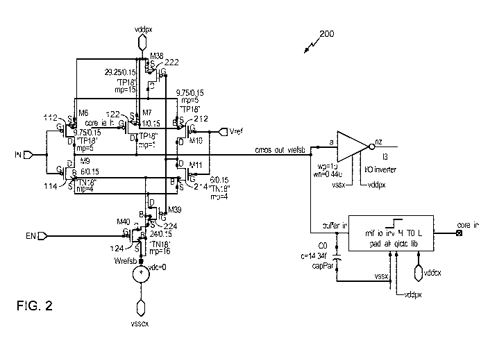
the like. For higher frequency operation, such as from 200MHz to 533MHz,
several
kinds of Vref-based single-ended pseudo-differential input receiver as shown
in
Figure 2 have been used with different Vref values, such as one-half the
supply
voltage without parallel termination or 70% supply voltage with a Vddq-
termination.
[0004] To cover wide-range frequency and support for Vref, such as
required
for receiver implementations in support of a low power Double Data Rate (DDR2)
interface, a simple solution is to configure multiple parallel input receivers
and to turn
on only one receiver based on the Vref value. This approach, however, is not
desirable in terms of area and power. Additionally, the multiple parallel
receiver
implementation suffers from performance degradation that can be attributable
to the
increased input capacitance, Cin, and the increased input-path delay due to
the
added mux.
CA 02686967 2013-01-23
74769-2646
2
BRIEF DESCRIPTION OF THE DRAWINGS
[0005] Figure 1 is a simplified schematic diagram of an exemplary
embodiment of a
CMOS receiver without support for Vref.
[0006] Figure 2 is a simplified schematic diagram of an exemplary
embodiment of a
pseudo-differential receiver with support for Vref.
[0007] Figure 3 is a simplified schematic diagram of an exemplary
embodiment of a
Vref adjustable self biased pseudo-differential receiver.
[0008] Figure 4 is a simplified schematic diagram of an exemplary
embodiment of a
Vref adjustable self biased pseudo-differential receiver.
[0009] Figures 5a-5f are simplified diagrams of performance curves
comparing
various exemplary receiver embodiments.
[0010] Figure 6 is a simplified schematic diagram of an exemplary
embodiment of a
Vref adjustable self biased NMOS pseudo-differential receiver.
[0011] Figure 7 is a simplified schematic diagram of an exemplary
embodiment of a
Vref adjustable self biased pseudo-differential receiver.
[0012] Figures 8a-8f are simplified diagrams of performance curves
comparing
various exemplary receiver embodiments.
[0013] Figure 9 is a simplified flowchart of an exemplary embodiment
of a method of
self biasing pseudo-differential receiver.
DETAILED DESCRIPTION
[0013a] According to one aspect of the present invention, there is
provided a variable
range logic threshold enabled input receiver apparatus, the apparatus
comprising: a logic
device; a logic threshold configuration coupled in parallel to the logic
device and configured
CA 02686967 2013-01-23
74769-2646
2a
to receive a variable logic threshold value and configure the logic device for
the variable logic
threshold value; and a helper device configured to receive the variable logic
threshold value
and configured to provide a bias current path from a power supply to the logic
device distinct
from a bias current path provided from the power supply to the logic device by
the logic
threshold configuration.
[0013b] According to another aspect of the present invention, there is
provided an
integrated circuit having the variable range logic threshold enabled input
receiver apparatus as
described above or detailed below.
[0013c] According to still another aspect of the present invention,
there is provided a
variable range logic threshold enabled input receiver apparatus, the apparatus
comprising: a
CMOS inverter; a Vref CMOS pair, including: a Vref PMOS FET having a source
common to
a PMOS source of the CMOS inverter; and a Vref NMOS FET having a drain common
to a
drain of the Vref PMOS FET, a source common to a NMOS source of the CMOS
inverter and
configured to receive a logic threshold value; a PMOS pull up FET having a
gate coupled to
the common drain of the Vref CMOS pair and a drain coupled to the common PMOS
source
connection so that the PMOS pull up FET is coupled to pull up the Vref CMOS
pair; an
NMOS pull down FET having a gate coupled to the common drain of the Vref CMOS
pair
and coupled to pull down the common NMOS source connection; and a helper PMOS
FET
having a gate configured to receive the logic threshold value and configured
to pull up the
common PMOS source connection.
[0013d] According to yet another aspect of the present invention,
there is provided a
method of configuring a self biasing logic input receiver, the method
comprising: configuring
a logic device; configuring logic threshold devices coupled in parallel to the
logic device to
receive a variable logic threshold value and configure the logic device for
the variable logic
threshold value; and configuring a helper device to receive the variable logic
threshold value
and configured to provide a bias current path from a power supply to the logic
device distinct
from a bias current path provided from the power supply to the logic device by
the logic
threshold devices.
CA 02686967 2013-01-23
74769-2646
2b
[0013e] According to a further aspect of the present invention, there
is provided a
variable range logic threshold enabled input receiver apparatus, the apparatus
comprising: a
CMOS inverter; means coupled in parallel to the CMOS inverter for receiving a
variable logic
threshold value and configuring the CMOS inverter for the variable logic
threshold value; and
means for receiving the variable logic threshold value and providing a bias
current path from a
power supply to the CMOS inverter distinct from a bias current path provided
from the power
supply to the CMOS inverter by the means for receiving a variable logic
threshold value.
[0014] The word "exemplary" is used herein to mean "serving as an
example,
instance, or illustration." Any embodiment described herein as "exemplary" is
not necessarily
to be construed as preferred or advantageous over other embodiments.
[0015] The detailed description set forth below in connection with
the appended
drawings is intended as a description of exemplary embodiments of the present
invention and
is not intended to represent the only embodiments in which the present
invention can be
practiced. The term "exemplary" used throughout this description means
"serving as an
example, instance, or illustration," and should not necessarily be construed
as preferred or
advantageous over other exemplary embodiments. The detailed description
includes specific
details for the purpose of providing a thorough understanding of the exemplary
embodiments
of the invention. It will be apparent to those skilled in the art that the
exemplary embodiments
of the invention may be
CA 02686967 2009-11-09
WO 2008/150794 PCT/US2008/064968
3
practiced without these specific details. In some instances, well known
structures and
devices are shown in block diagram form in order to avoid obscuring the
novelty of the
exemplary embodiments presented herein.
[0016] It is desirable to have only one configuration of a wide-frequency-
range Vref-
adjustable input receiver. The receiver configuration can be made to operate
over a
wide frequency range and over a wide range of Vref values. The performance of
the
receiver can be easily adjusted with changes that only have minimal effects on
die area
and power consumption.
[0017] Figure 1 is a simplified schematic diagram of an exemplary
embodiment of a
conventional CMOS receiver 100 without Vref. The conventional CMOS receiver
100
of Figure 1 can be implemented using conventional thick devices or thin
devices.
[0018] The conventional CMOS receiver 100 includes a conventional
complementary
FET pair configured as a CMOS inverter that includes a PMOS FET 112 stacked on
an
NMOS FET 114. The source of the PMOS FET 112 is coupled to Vdd and the drain
is
common with the drain of the NMOS FET 114, which operates as the output of the
CMOS inverter. The gate of the PMOS FET 112 is common with the gate of the
NMOS FET 114 and serves as the input to the CMOS receiver 100.
[0019] The source of the NMOS FET 114 can be coupled to Vss or optionally
to the
drain connection of an NMOS enable FET 124. The source of the NMOS enable FET
124 is coupled to Vss and the gate receives an enable control signal.
Similarly, a PMOS
enable FET 122 can be configured to pull up the output of the CMOS inverter
when the
inverter is not enabled. The source of the PMOS enable FET 122 is coupled to
Vdd and
the drain is coupled to the output of the CMOS inverter. The gate of the PMOS
enable
FET 122 is configured to receive the enable control signal.
[0020] The conventional CMOS receiver 100 of Figure 1 does not support a
Vref input,.
The inability to support a variable Vref value makes the conventional CMOS
receiver
100 less desirable for operation at higher frequencies with small swing input
aligned to
Vref-level. The Vref value can be considered the nominal logic threshold, and
the logic
transitions from low-high or high-low are often specified in terms of a Vref
value when
the receiver supports Vref. Support for an externally controllable Vref value
may be
desirable in order to compensate or otherwise interface with a bus or device
that may
not operate at precisely the same supply voltage used by the CMOS receiver 100
or to
otherwise compensate for effects of an electrical bus or interface. Indeed,
some
memory interface standards expressly set forth a range of values for Vref.
CA 02686967 2009-11-09
WO 2008/150794 PCT/US2008/064968
4
[0021] The exemplary pseudo-differential receiver 200 embodiment of Figure
2 includes
provisions for accepting a Vref value. The exemplary pseudo-differential
receiver 200
embodiment of Figure 2 can be based on the same CMOS inverter described in the
exemplary embodiment of Figure 1. A PMOS FET 112 is stacked on an NMOS FET
114, and the two FETs share a common gate connection as the inverter input.
[0022] A Vref CMOS pair is positioned substantially in parallel to the
CMOS inverter.
The parallel configuration refers to begin connected electrically in parallel,
such that the
input current connections for the Vref CMOS pair and the CMOS inverter are
common
as are the output current connections.
[0023] A Vref value drives the input to the Vref CMOS pair. The Vref value
is
typically received from an external interface to an integrated circuit,
although the Vref
value may also be generated internal to an integrated circuit. Typically, the
Vref value
represents a logic threshold, setpoint, or trip point. The value of the logic
threshold may
be adjusted to accommodate interfacing with various devices that may not
operate on
the same voltage supply as the input receiver. The Vref CMOS pair includes a
PMOS
Vref FET 212 stacked on an NMOS Vref FET 214. The PMOS Vref FET 212 and
NMOS Vref FET 214 have common gate connections, which are configured to
receive
the reference voltage, Vref.
[0024] The source connection of the PMOS Vref FET 212 is common with the
source
of the PMOS FET 112 of the CMOS inverter. The common source connections are
coupled to the drain of a pull up PMOS FET 222. The source of the pull up PMOS
FET
222 is coupled to Vdd, while the gate is coupled to the common drain
connections of the
Vref CMOS pair.
[0025] The source connection of the NMOS Vref FET 214 is common with the
source
of the NMOS FET 114 of the CMOS inverter. A pull down NMOS FET 224 has a
drain connected to the common source connections and has a source connected to
Vss
or optionally to the drain of the NMOS enable FET 124. The gate of the pull
down
NMOS FET 224 is coupled to the common drain connection of the Vref CMOS pair.
[0026] The Vref CMOS pair in combination with the pull up PMOS FET 222 and
the pull
down NMOS FET 224 operates to control the logic threshold or trip point of the
CMOS
inverter, and controls the bias current through the CMOS inverter based on the
relationship
of the input voltage to the Vref value. However, the conventional Vref-based
pseudo-
differential receiver 200 can not always be well-biased to meet high
performance operation
over a wide-range of Vref, particularly when Vref is close to Vss or Vdd.
CA 02686967 2011-10-07
74769-2646
[0027] The conventional approach for addressing a range of Vref values
is to produce a
number of input receivers in parallel and to select the input receiver based
on the Vref
operating value. Configuring multiple input receivers in parallel and
selecting one of
the input receivers based on the value of Vref is an inefficient manner of
providing
support for wide input frequency range and Vref range. The CMOS input
receivers and
methods disclosed herein implement a more efficient solution that utilizes a
single input
receiver implementation that is configurable to support a wide range of input
frequencies and a wide range of Vref values.
[0028] Figure 3 is a simplified schematic diagram of a Vref adjustable
self biased
pseudo-differential input receiver 300. The self biased pseudo-differential
input
receiver 300 includes provisions for accepting a Vref value to a CMOS pair
that is in
parallel to the active CMOS logic pair of the CMOS receiver 300. However,
unlike the
Vref based pseudo-differential receiver exemplary embodiment of Figure 2, the
self
biased pseudo-differential receiver 300 further includes a helper PMOS FET
310,
alternatively configured as an enabled stacked PMOS helper, that pulls up the
source of
the PMOS FET112 in the active CMOS pair. The helper PMOS FET 310 has its
source
coupled to Vdd and its drain coupled to the source of the PMOS FET 112 in the
active
CMOS logic pair, which is also common to the source of the Vref PMOS FET 212.
Thus, the self biased pseudo-differential input receiver 300 can be configured
substantially identical to the CMOS receiver exemplary embodiment of Figure 2
with
the addition of the helper PMOS FET 310, which can be referred to in the
alternative as
a current helper FET or 'bias helper FET.
[0029] The source of the helper PMOS FET 310 is coupled to Vdd and its
drain coupled
to the source of the PMOS FET 112 in the CMOS logic pair. The gate of the
helper
PMOS FET 310 receives the Vref value. Thus, the helper PMOS FET 310
effectively
monitors the Vref line and provides a path for Ibias current for the CMOS
inverter..
The addition of the helper PMOS FET 310 permits the pseudo-differential
receiver 300
to operate substantially as a conventional CMOS receiver when Vref is at or
near zero
volts. Also, the CMOS receiver 300 exemplary embodiment of Figure 3 exhibits
performance that is better than that of the conventional CMOS receiver of
Figure 1,
because the CMOS receiver 300 of Figure 3 can operate with non-zero Vref
values.
[0030] The addition of the PMOS FET 310 to a Vref-enabled pseudo-
differential
receiver permits the pseudo-differential receiver 300 to perform comparable to
a Vref-
enabled pseudo-differential receiver, such as the receiver exemplary
embodiment of
CA 02686967 2009-11-09
WO 2008/150794 PCT/US2008/064968
6
Figure 2, under conditions where Vref is approximately 0.5 Vdd. Thus, the
pseudo-
differential receiver 300 configuration of Figure 3 can operate over a range
of Vref of
approximately from Vss to 50% Vdd.
[0031] Figure 4 illustrates another exemplary embodiment of a pseudo-
differential input
receiver 400. The input receiver exemplary embodiment of Figure 4, as well as
the
exemplary embodiments illustrated in other figures, may be configured using
thick
devices as well as thin devices. The pseudo-differential receiver 400
exemplary
embodiment of Figure 4 is configured similar to the pseudo-differential input
receiver
exemplary embodiment illustrated in Figure 3. The pseudo-differential input
receiver
400 includes the helper PMOS FET 310 as illustrated in the exemplary
embodiment of
Figure 3, and also includes an NMOS helper configuration 420.
[0032] The NMOS helper configuration 420 permits Vref-based CMOS receiver
400 to
work with programmability on bias currents and trip-point over a range of
Vref=(0.5-0.7)Vdd. Thus, when the NMOS helper configuration 420 is used in
combination with the helper PMOS FET 310, the CMOS receiver 400 can operate
over
a range Vref values spanning approximately from Vss to 70% Vdd.
[0033] The NMOS helper configuration 420 includes a stacked configuration
of two
NMOS FETs 422 and 424. A helper NMOS FET 422 is implemented in a stacked
configuration with an enable NMOS FET 424. In the stacked configuration, the
source
of the helper NMOS FET 422 is connected to the drain of the enable NMOS FET
424 in
a series connection, such that current flow through the helper NMOS FET 422 is
inhibited when the enable NMOS FET 424 is switched off.
[0034] The gate of the enable NMOS FET 424 is configured to receive an
enable
control signal, such as an interface enable control signal. The gate of the
helper NMOS
FET 422 is configured to receive the Vref value and thus operates to further
regulate the
current through the CMOS inverter based in part on the value of the Vref
voltage.
[0035] The pseudo-differential input receiver 400 also may include an
active input
termination 430. The performance of the CMOS receiver 400 may be adjusted
based on
a ratio of the output driver's impedance to parallel on/off-die termination
impedance.
Although the input of the receiver 400 exemplary embodiment of Figure 4 is
illustrated
as having an active Vccq termination 430 at the input to the CMOS receiver
400, such a
termination is not always needed, and the termination may be omitted in other
configurations.
CA 02686967 2009-11-09
WO 2008/150794 PCT/US2008/064968
7
[0036] Figures 5a-5f are simplified diagrams of performance curves
comparing various
receiver exemplary embodiments. Figure 5a illustrates bias currents with
respect to Vin
for the receiver exemplary embodiments illustrated in Figures 1-4 when Vref is
set to
OV. Because the Vref value is set to 0 volts, the bias current in the
exemplary
embodiment of Figure 2 is substantially limited.
[0037] Figure 5b illustrates the corresponding voltage transfer function
of Vout with
respect to Vin for the receiver exemplary embodiments with Vref set to OV. As
can be
seen from the voltage transfer function of Figure 5b, the conventional Vref
enabled
pseudo-differential receiver 200 exemplary embodiment of Figure 2 performs
poorly
when the Vref value is near zero.
[0038] Figure 5c illustrates bias currents with respect to Vin for the
receiver exemplary
embodiments illustrated in Figures 1-4 when Vref is set to approximately one-
half the
Vdd value for those exemplary embodiments supporting a Vref value. As can be
seen,
the addition of the helper FETs increase the amount of current that steady
state bias
current flowing through the input receiver.
[0039] Figure 5d illustrates the corresponding voltage transfer function
of Vout with
respect to Vin for the receiver exemplary embodiments with Vref=(0.5)Vdd. The
receivers forming the basis of the performance curves of Figures 5a-5f utilize
a Vdd of
1.2V. Thus, the Vref value in Figures 5b and 5c correspond to approximately
0.6V.
Because this logic threshold represents substantially a standard
configuration, each of
the exemplary embodiments performs satisfactorily, as one would assume.
[0040] Figure 5e illustrates bias currents with respect to Vin for the
receiver exemplary
embodiments illustrated in Figures 1-4 when Vref is set to greater than one-
half the Vdd
value for those exemplary embodiments supporting a Vref value.
[0041] Figure 5f illustrates the corresponding voltage transfer function
of Vout with
respect to Vin for the receiver exemplary embodiments with Vref=0.7V,
corresponding
to approximately 0.58Vdd. This level of Vref may be greater than is
conventionally
supported by a conventional input receiver, even one that accepts a Vref
input.
[0042] As can be seen by the performance curves of Figures 5e and 5f, the
CMOS
receiver exemplary embodiment of Figure 1, which does not support a Vref
value, fails to
enable adjusting the setpoint or logic threshold of the voltage transfer
function. The
CMOS input exemplary receiver embodiments of Figures 2-4 closely tracks the
increase
in the Vref value. However, as can be seen in the voltage transfer function
curves of
Figure 5f, the exemplary pseudo-differential input receiver embodiments of
Figures 2 and
CA 02686967 2011-10-07
74769-2646
8
3 can support the increased Vref value, but do not pull down near ground when
outputting
the low logic state. The CMOS input receiver of Figure 4 having the helper
NMOS
configuration enables the output voltage to pull nearer to zero volts when the
input is high.
[0043] The Vref improvements are not limited to use with a pseudo-
differential input
receiver, but may be applicable to other input receivers based on other
configurations.
Figure 6 is a simplified schematic diagram of an exemplary embodiment of a
Vref
adjustable NMOS receiver 600.
[0044] A first NMOS FET 614 is configured as the logic gate. The gate
of the first
NMOS FET 614 is configured to receive the input voltage. The source of the
first
NMOS FET 614 is coupled to the drain of an enable NMOS FET 624. The source of
the enable NMOS FET 624 is coupled to Vss or ground, and the gate of the
enable
NMOS FET 624 is configured to receive an active high enable signal.
[0045] The drain of the first NMOS FET 614 represents the logic output
from the input
receiver 600. The drain of the first NMOS FET 614 is coupled to the drain of
an enable
PMOS FET 622 that operates to pull up the output voltage when the input
receiver is
not enabled. The source of the enable PMOS FET 622 is coupled to Vdd, while
its gate
receives the active high enable signal.
[0046] The configuration of devices implemented to support the Vref
input include a
second NMOS FET 630 configured as a Vref NMOS FET. The gate of the second
NMOS FET 630 receives the Vref signal, while the source of the second NMOS FET
630 is common with the source of the first NMOS FET 614. The drain of the
second
NMOS FET 630 is coupled to the gate connections of two separate pull-up FETs.
[0047] A first PMOS pull up FET 632 has its source coupled to Vdd, a
gate coupled to
the drain of the second NMOS FET 630, and a drain coupled to the drain of the
first
NMOS FET 614. A second PMOS pull up FET 634 has its source coupled to Vdd, and
both its gate and drain connections coupled to the drain of the second NMOS
FET 630.
[0048] The input receiver 600 includes a helper FET configuration
including two helper
FETs, 642 and 644. The helper FETs 642 and 644 permit the input receiver to
operate
over a wider range of Vref values, including Vref at or near 0 volts.
[0049] A first helper PMOS FET 642 pulls up the logic NMOS FET 614 that
has its
gate configured to receive the input signal. The gate of the first helper PMOS
FET 642
is connected to Vref. The source of the first helper PMOS FET 642 is coupled
to Vdd,
while the drain of the first helper PMOS FET 642 is coupled to the drain of
the logic
NMOS FET 614.
_
CA 02686967 2009-11-09
WO 2008/150794 PCT/US2008/064968
9
[0050] The second helper PMOS FET pulls up the Vref or second NMOS FET 630
that
has its gate controlled by the Vref value. The gate of the second helper PMOS
FET 644
is also connected to Vref. The source of the second helper PMOS FET 644 is
coupled
to Vdd, while the drain of the second helper PMOS FET 644 is coupled to the
drain of
the Vref NMOS FET 630.
[0051] The helper FETs operate in much the same manner as when configured
to
support a CMOS logic gate. The PMOS helper FET configuration operates to
supply
bias current to the NMOS logic gate even under conditions where the Vref value
is low
or near 0 volts.
[0052] Figure 7 is a simplified schematic diagram of an exemplary
embodiment of a
Vref adjustable self biased CMOS receiver 700. The configuration of the CMOS
receiver 700 of Figure 7 is similar to the configuration of the CMOS receiver
of Figure
4. However, the pseudo-differential receiver 700 of Figure 7 includes a Vref
level
detector 740 rather than just a helper NMOS FET configuration as in the
exemplary
pseudo-differential receiver embodiment of Figure 4.
[0053] The pseudo-differential input receiver 700 of Figure 7 is based on
the CMOS
receiver of Figure 2. A PMOS FET 112 is stacked on an NMOS FET 114, and the
two
FETs share a common gate connection as the inverter input.
[0054] A Vref CMOS pair is positioned substantially in parallel to the
CMOS inverter.
The Vref CMOS pair includes a PMOS Vref FET 212 stacked on an NMOS Vref FET
214. The PMOS Vref FET 212 and NMOS Vref FET 214 have common gate
connections, which are configured to receive the reference voltage, Vref.
[0055] The source connection of the PMOS Vref FET 212 is common with the
source
of the PMOS FET 112 of the CMOS inverter. The common source connections are
coupled to the drain of a pull up PMOS FET 222. The source of the pull up PMOS
FET
222 is coupled to Vdd, while the gate is coupled to the common drain
connections of the
Vref CMOS pair.
[0056] The source connection of the NMOS Vref FET 214 is common with the
source
of the NMOS FET 114 of the CMOS inverter. A pull down NMOS FET 224 has a
drain connected to the common source connections and has a source connected to
Vss
or optionally to the drain of the NMOS enable FET 124. The gate of the pull
down
NMOS FET 224 is coupled to the common drain connection of the Vref CMOS pair.
[0057] The pseudo-differential receiver 700 includes a plurality of helper
PMOS FETs
712 and 714. A first helper PMOS FET 712 has its gate coupled to Vref, while a
second
CA 02686967 2011-10-07
7 4 7 6 9 ¨ 2 6 4 6
helper PMOS FET 714 has its gate coupled to a signal from the Vref level
detector 740.
The source of the first helper PMOS FET 712 is coupled to Vdd while the drain
of the
first helper PMOS FET 712 is coupled to the common source connections of the
CMOS
logic gate and the Vref CMOS pair.
[0058] The source of the second helper PMOS FET 714 is coupled to Vdd.
The drain
of the second helper PMOS FE1 714 ' is coupled to the common source
connections of
the CMOS logic gate and the Vref CMOS pair.
[0059] The Vref level detector 740 includes an NMOS FET 742 in stacked
configuration with an NMOS enable FET 744. The gate of the NMOS FET 742 is
configured to receive the Vref value. The source of the NMOS FET 742 is
coupled to
the drain of the NMOS enable FET 744. The gate of the NMOS enable FET 744 is
configured to receive the enable signal, while the source of the NMOS enable
FET 744
is coupled to Vss.
[0060] The drain of the NMOS FET 742 is coupled to a PMOS pull-up FET
746 having
its source coupled to Vdd. The gate of the PMOS pull-up FET 746 is coupled to
the
drain of the NMOS FET 742. The drain of the NMOS FET 742 is also coupled to
the
gate of the second helper PMOS FET 714.
[0061] The Vref-level detector 740 of the exemplary pseudo-differential
receiver 700
embodiment of Figure 7 enables the CMOS receiver to work more efficiently over
a
wide range of Vref values than the pseudo-differential receiver configuration
of Figure
4. The Vref-level detector 740 maintains the effectiveness of the bias helper
FETs over
the entire Vref range to enable the pseudo-differential receiver 700 of Figure
7 to
operate over a Vref range of substantially from Vss to 72% Vdd, which
corresponds to
approximately 0-0.864 volts for a 1.2V Vdd value.
[0062] Figures 8a-8f are simplified diagrams of performance curves
comparing various
exemplary receiver embodiments. Figures 8a and 8b illustrate, respectively,
the bias
current with respect to Vin and the voltage transfer function of Vout with
respect to Vin
for the exemplary input receiver embodiments of Figures 1, 4, 6, and 7 when
Vref is set
to OV. As can be seen from Figure 8a, the exemplary NMOS receiver embodiment
continues to conduct once the NMOS FET is biased to an ON condition.
[0063] Figures 8c and 8d illustrate, respectively, the bias current with
respect to Vin
and the voltage transfer function of Vout with respect to Vin for the
exemplary input
receiver embodiments of Figures 1, 4, 6, and 7 when Vref is set to
approximately one-
half the Vdd voltage, which is approximately 0.6V for a Vdd of 1.2V. The
exemplary
CA 02686967 2009-11-09
WO 2008/150794 PCT/US2008/064968
11
CMOS receiver embodiment of Figure 1 does not accept a Vref value, and thus
its
performance remains the same as in Figures 8a and 8b.
[0064] Figures 8e and 8f illustrate, respectively, the bias current with
respect to Vin and
the voltage transfer function of Vout with respect to Vin for the exemplary
input
receiver embodiments of Figures 1, 4, 6, and 7 when Vref is set to a value
greater than
one-half the Vdd voltage. In the performance curves of Figures 8e and 8f, the
value of
Vref is set to approximately 0.8V.
[0065] As can be seen by the performance curves of Figure 8f, only the
Vref-detecting
CMOS receiver of Figure 7 is able to closely track the high Vref level of 0.8V
while
maintaining an acceptable current level.
[0066] Each of the exemplary input receiver embodiments of Figures 3-4 and
Figures 6-
7 can be utilized as an input receiver for an interface of an integrated
circuit or module.
For example, each address or data input to a memory module or memory
integrated
circuit can be configured with an input receiver as described herein in order
to enable
operation over a wide range of Vref and frequency values.
[0067] Figure 9 is a simplified flowchart of an exemplary embodiment of a
method 900
of configuring a self biasing a CMOS receiver. The method 900 can be
performed, for
example, when manufacturing or designing an integrated circuit having an input
receiver described herein or when configuring a module having the input
receiver
described herein.
[0068] The method begins at block 910 where the designer configures a
logic device.
Most commonly, the designer will configure a CMOS logic inverter , which is
the
baseline for many logic devices. However, the methods and input receiver
exemplary
embodiments are not limited to CMOS configurations, and a designer may
configure,
for example, a NMOS inverter.
[0069] The designer proceeds to block 920 and configured Vref logic
devices in order
to permit support for a varying Vref level. As described above, the Vref level
may be
set external to an integrated circuit.
[0070] The Vref logic device or devices include a Vref device positioned
substantially in
parallel to the logic device. In the exemplary embodiment, a Vref CMOS pair is
positioned substantially in parallel to the CMOS inverter, which is the CMOS
logic gate.
[0071] The Vref logic devices also include a pull up FET, such as a pull
up PMOS FET
that has its gate controlled by the common drain connection of the Vref CMOS
pair.
The Vref logic devices also include a pull down NMOS FET that has its gate
controlled
CA 02686967 2009-11-09
WO 2008/150794 PCT/US2008/064968
12
by the common drain connection of the Vref CMOS pair. The pull up and pull
down
FETs control the amount of current that flows through the CMOS logic gate.
[0072] The designer proceeds to block 924 and optionally configures one or
more
enable devices. The enable devices permit the input receiver to be placed in
an inactive
high impedance or terminated state. The enable devices can also be configured
to
supply a constant logic state at its output in order to provide a stable logic
output and
not float to an indeterminate value when not enabled. Although the exemplary
embodiments illustrated herein implement an active high enable signal, the
enable
devices may be implemented to operate using an active high or active low
enable signal.
[0073] After configuring the enable devices, if any, the designer proceeds
to block 930
and configures one or more helper devices. As shown in the exemplary
embodiments of
Figures 3-4 and 6-7, the helper devices can include one or more PMOS helpers
as well
as one or more NMOS helpers.
[0074] Each PMOS helper can be positioned substantially in parallel to the
pull up
PMOS FETs and can have a gate controlled by the Vref value and can operate to
pull up
the logic output. Each NMOS helper can be positioned substantially in parallel
to an
NMOS pull down FET and can have a gate coupled to the Vref value.
[0075] The designer proceeds to block 940 and optionally configures a Vref
detector
that can also operate as a bias current amplifier. As illustrated in the
exemplary
embodiment of Figure 7, the Vref detector can include an NMOS gate driven by
the
Vref value. The drain of the NMOS gate is coupled to a PMOS pull-up FET. The
drain
of the NMOS gate is also coupled to the gate of a helper PMOS FET that is
distinct
from other helper PMOS FETs that may be driven by the Vref value.
[0076] The use of helper FETs enable the input receiver to operate over a
wider range
of Vref values. A pull up helper PMOS FET permits current to flow in the logic
device
when the Vref value is low, such as when it is near or at 0 volts. The pull
down helper
FETs assist in pulling down the low output logic level when the Vref value is
higher
than is conventionally used.
[0077] Apparatus and methods for implementing an input receiver that is
capable of
operating over a large range of Vref values and over a wide range of
frequencies is
described herein. The wide range Vref enabled input receiver permits a single
input
receiver to be used in contrast to conventional teachings of having several
parallel
configurations of input receivers, each optimized for a particular range of
Vref and
frequency of operation.
CA 02686967 2009-11-09
WO 2008/150794 PCT/US2008/064968
13
[0078] Those of skill in the art would understand that information and
signals may be
represented using any of a variety of different technologies and techniques.
For
example, data, instructions, commands, information, signals, bits, symbols,
and chips
that may be referenced throughout the above description may be represented by
voltages, currents, electromagnetic waves, magnetic fields or particles,
optical fields or
particles, or any combination thereof.
[0079] Those of skill would further appreciate that the various
illustrative logical
blocks, modules, circuits, and algorithm steps described in connection with
the
embodiments disclosed herein may be implemented as electronic hardware,
computer
software, or combinations of both. To clearly illustrate this
interchangeability of
hardware and software, various illustrative components, blocks, modules,
circuits, and
steps have been described above generally in terms of their functionality.
Whether such
functionality is implemented as hardware or software depends upon the
particular
application and design constraints imposed on the overall system. Skilled
artisans may
implement the described functionality in varying ways for each particular
application,
but such implementation decisions should not be interpreted as causing a
departure from
the scope of the exemplary embodiments of the invention.
[0080] The various illustrative logical blocks, modules, and circuits
described in
connection with the embodiments disclosed herein may be implemented or
performed
with a general purpose processor, a Digital Signal Processor (DSP), an
Application
Specific Integrated Circuit (ASIC), a Field Programmable Gate Array (FPGA) or
other
programmable logic device, discrete gate or transistor logic, discrete
hardware
components, or any combination thereof designed to perform the functions
described
herein. A general purpose processor may be a microprocessor, but in the
alternative, the
processor may be any conventional processor, controller, microcontroller, or
state
machine. A processor may also be implemented as a combination of computing
devices, e.g., a combination of a DSP and a microprocessor, a plurality of
microprocessors, one or more microprocessors in conjunction with a DSP core,
or any
other such configuration.
[0081] The steps of a method or algorithm described in connection with the
embodiments disclosed herein may be embodied directly in hardware, in a
software
module executed by a processor, or in a combination of the two. A software
module
may reside in Random Access Memory (RAM), flash memory, Read Only Memory
(ROM), Electrically Programmable ROM (EPROM), Electrically Erasable
CA 02686967 2011-10-07
74769-2646
14
Programmable ROM (EEPROM), registers, hard disk, a removable disk, a CD-ROM,
or
any other form of storage medium known in the art. An exemplary storage medium
is
'coupled to the processor such that the processor can read information from,
and write
information to, the storage medium. In the alternative, the storage medium may
be
integral to the processor. The processor and the storage medium may reside in
an
ASIC. The ASIC may reside in a user terminal. In the alternative, the
processor and the
storage medium may reside as discrete components in a user terminal.
[0082] In one or more exemplary embodiments, the functions described may
be
implemented in hardware, software, firmware, or any combination thereof. If
implemented in software, the functions may be stored on or transmitted over as
one or
more instructions or code on a computer-readable medium. Computer-readable
media
includes both computer storage media and communication media including any
medium
that facilitates transfer of a computer program from one place to another. A
storage
media may be any available media that can be accessed by a computer. By way of
example, and not limitation, such computer-readable media can comprise RAM,
ROM,
EEPROM, CD-ROM or other optical disk storage, magnetic disk storage or other
magnetic storage devices, or any other medium that can be used to carry or
store desired
program code in the form of instructions or data structures and that can be
accessed by a
computer. Also, any connection is properly termed a computer-readable medium.
For
example, if the software is transmitted from a website, server, or other
remote source
using a coaxial cable, fiber optic cable, twisted pair, digital subscriber
line (DSL), or
wireless technologies such as infrared, radio, and microwave, then the coaxial
cable,
fiber optic cable, twisted pair, DSL, or wireless technologies such as
infrared, radio, and
microwave are included in the definition of medium. Disk and disc, as used
herein,
includes compact disc (CD), laser disc, optical disc, digital versatile disc
(DVD), floppy
disk and blu-ray disc where disks usually reproduce data magnetically, while
discs
reproduce data optically with lasers. Combinations of the above should also be
included
within the scope of computer-readable media.
[0083] The previous description of the disclosed exemplary embodiments
is provided to
enable any person skilled in the art to make or use the present invention.
Various
modifications to these exemplary embodiments will be readily apparent to those
skilled in
the art, and the generic principles defined herein may be applied to other
embodiments
without departing from the scope of the invention. Thus, the present invention
is
CA 02686967 2009-11-09
WO 2008/150794 PCT/US2008/064968
not intended to be limited to the embodiments shown herein but is to be
accorded the
widest scope consistent with the principles and novel features disclosed
herein.