Note: Descriptions are shown in the official language in which they were submitted.
CA 02687120 2009-11-06
WO 2008/134889 1 PCT/CA2008/000861
TITLE
Ultra High Speed Signal Transmission/Reception
FIELD
The present patent document relates to a communication link for transmitting
an
electric signal between electronic devices
BACKGROUND
Communication within or between integrated circuits is a fundamental attribute
of
electronic devices. Such communication can involve communication between
similar or
different chips on a laminate printed circuit board or similar substrate
material or within
the chip itself. The chips themselves may be manufactured using similar or
different
technologies. Recent trends show demand for high-speed communication
technology is
increasing and is critical to address the demand of higher bandwidth and to
accommodate
testing of high-speed devices at the device and circuit levels. In addition to
this, as
devices are increasing in complexity there is increasing need to lower the
power
consumption, decrease the size and reduce the overall system cost. This has
created a
significant momentum in the area for high-speed interfacing and interconnect.
In recent years interconnect technology has evolved from parallel digital to
serial
based communication to enable transfer of data in the gigabit range using
direct wiring or
external transform coupling. Conventional serial I/O cells require ESD
(Electro Static
Discharge) protection circuits resulting in less power-efficiency, speed
limitations, and
larger pad size. Furthermore, within a modest power budget, signals can only
be
consistently and reliably transmitted over a short data path, making them
prone to
interference and of limited operating range for high-speed/frequency. It is
possible to
overcome the signal limits but at the expense of increased power. For example
it is
possible to go 10 Gbits/second using the lOG Ethernet serial wired link.
However, such
transceivers require up to 15 Watts of power which is not a practical
communications
method except for point to point communication for a small number of channels.
Power
consumption is a major limiting factor where multiple channels of I/O are
required thus
SUBSTITUTE SHEET (RULE 26)
CA 02687120 2009-11-06
2
WO 2008/134889 PCT/CA2008/000861
each individual I/O channel must meet a prescribed power budget many times
lower than
that of the proposed lOG standard. Large amounts of power are required as a
consequence of techniques used to address signal degradation which increases
with the
length of the data path. Data path length and its impact on signal integrity
is often a
major concern with prior art solutions. Examples of high-speed signal
communication
include transfer and/or sharing of data at chip-to-chip, chip-to-substrate,
and board-to-
board or backplane level and their converse.
The most commonly used methods of signal communication between electronic
devices include making physical, electrical contact between two nodes.
Electrical signals
may comprise DC or AC signals or both. Alternative methods to interconnect
nodes
include methods of AC coupling including capacitive and inductive techniques
where the
DC component is not available or where the DC component would add noise or
have
some other unwanted effect. Further, signals may be coupled using optical
methods,
magnetic methods, or radio frequency transmission/reception. While digital
communications between integrated circuits are of primary interest,
cominunication
involving both digital and analog signals is also needed.
Referring to FIG. 1 a, a conventional apparatus of an integrated circuit (IC
or chip)
10 is shown for input of a signal 14 sent from a first internal electronic
application
specific circuit 16 on the chip 10 to one or more pads 112. First application
specific
circuit 16 may be an output device or an input device such as a receiver for
receiving
signal 14 from an external source. Signal 14 may be digital or analog. Signal
14 is
conditioned as it is propagated toward pad 112 via a buffer 18. Electrostatic
discharge
protection (ESD) is provided by diodes 20 which divert ESD currents to ground
or power
supply or other protective circuits. The protective circuits are intended to
absorb and
dissipate destructive energy originating from an external source coming in
electrical
contact with pad 112 before reaching sensitive internal application specific
circuits 16.
Such apparatus 10 has limitations. Compensation is required when buffers 18
and
pad 112 have different characteristics. Electrostatic discharge diodes 20 and
associated
SUBSTITUTE SHEET (RULE 26)
CA 02687120 2009-11-06
3
WO 2008/134889 PCT/CA2008/000861
protective circuits exhibit a large amount of parasitic capacitance and thus
apparatus 10
introduces a large amount of capacitance into the signal path. The signal
energy is
absorbed by the parasitic capacitance and dissipated as heat as signal 14 is
propagated
toward pad 112. Generally, the amount of signal loss increases with frequency.
Further,
signal 14 is delayed in time as it is propagated by the chain of buffers 18.
The
compensation and protection thus provided lowers the energy of wanted signals
14
coming from or going between the internal circuits and the external pad and,
by
extension, lowers available signal levels at a far transmitter or receiver.
Prior art I/O cells involve use of protective diodes and passive and active
elements to absorb and attenuate destructive voltages and currents. These
typically
involve active structures, which load the I/O cell. For example, it is known
that a typical
protection diode structure has an equivalent capacitance of approximately 1
pF. The
effect of a 1 pF capacitance in the signal path of a 2 GHz signal would be an
effective
load of 88 ohms per wire In a differential signalling schema this would
present an
equivalent load of 44 ohm compared to a typical transmission impedance of 50
ohms. In
other words there is more energy used (in this case) overcoming the load of
the protection
system than is used to send the active signals, and so the signal path
requires additional
amplification to compensate for the signal loss. Consequently, in our example,
the system
requires twice the area and consumes twice the power. While this case is a
simplification,
it is illustrative of the problems that the current practices involve. In
fact, if an I/O system
is to achieve higher data rates the problem is even worse: at twice the
frequency
approximately 80% of the driver's energy is consumed to overcome the load of
the
protection circuitry. -
Referring to FIG. lb, for conventional apparatus 10, an essentially similar
apparatus may be used for input of a signal through pad 112 to one or more
internal
circuits 24 or to an output device for transmission of signal 14 to an
external receiver.
FIG. 16a of United States Publication No. 2005/0271147 (Dupuis) entitled
"Transformer isolation for digital power supply" teaches a transformer
apparatus to
SUBSTITUTE SHEET (RULE 26)
CA 02687120 2009-11-06
WO 2008/134889 4 PCT/CA2008/000861
provide isolation between two integrated circuits located in close proximity
within a
single component package (Dupuis FIGS. 6, 15, 15a, 16, and 16a). While Dupuis
describes this as a high-speed data link, Dupuis actually uses a RF carrier
that is 20 times
the actual data (information) rate.
Similarly, Lane et al. in US 7064442 teaches an apparatus to provide isolation
between two integrated circuits located in close proximity within a single
component
package using a transformer, the transformer being located on a separate
circuit within
the same package. In this case, the external I/O signals interface directly
with active
electronic elements. Only for internal signals, after active electronics
processing, within
the package is the transformer/dielectric isolation formed and utilized.
In a similar manner as Lane et al, United States patent no. 5,952,849 (Haigh)
entitled "Logic isolator with high transient immunity", discloses an apparatus
to provide
isolation between two circuits using a transformer, where the transformer 38
is formed by
windings 36 and 42 on separate and discrete ferrite cores coupled by winding
42.
In a similar manner as Dupuis, United States patent no. 7,075,329 (Chen et
al.)
entitled "Signal isolators using micro-transfoirners" discloses an apparatus
that provides
isolation between two circuits using a transformer, where the transformer is a
separate
and discrete component. In Chen the external I/O pads or signals labelled
`input' and
`output' are interfaced with active electronics before and after the
transformer isolation
occurs and thus share the disadvantages of the Dupuis, Lane, Haigh and others.
The article H. Ishikuro, N. Miura, and T. Kuroda, "Wideband Inductive-coupling
Interface for High-performance Portable System", IEEE 2007 Custom Integrated
Circuits
Conference (CICC) shows an inductive coupling system in which chips are
designed with
inductive elements which enable direct face to face chip to chip
communications. In this
case the inductor on chip is an individual element and not combined with an
integrated
second inductive element on the same IC. This reference also shows separate
coils for
SUBSTITUTE SHEET (RULE 26)
CA 02687120 2009-11-06
WO 2008/134889 5 PCT/CA2008/000861
applications outside a package. In this case, the coils are fabricated
separately and
interfaced conductively with drive electronics.
United States Patent No. 5,361,277 (Grover) entitled "Method and apparatus for
clock distribution and for distributed clock synchronization" describes a
system in which
the timing is coordinated such that transmitters and receivers are coordinated
so that even
with distant systems a common time and clocking reference is obtained. In a
similar
manner, United States Patent No 5,243,703 (Fannwald et al.) entitled
"Apparatus for
synchronously generating clock signals in a data processing system" and United
States
Patent No. 5,954,804 (Farmwald et al.) entitled "Synchronous memory device
having an
internal register" describe a system in which timing is coordinated through
the knowledge
of clock edges following different paths. It should also be noted that the
Grover and
Farmwald patents describe wired systems such as direct wired memory or logic
systems
which further limit their systems. Wired systems as shown in the prior art are
encumbered by the need for ESD structures which limit speed and increase power
consumption.
United States Patent No. 6,882,239 (Miller et al.) entitled
"Electromagnetically
coupled interconnect system" describes electromagnetic coupling between
components in
a test system in which the IC is contained in a package with a separate
electromagnetic
(EM) coupler. In general, this patent provides loosely coupled signals in
which there is at
least 10dB of attenuation and further loss because of extra shielding. The
goal of Miller et
al. is to receive loosely coupled signals and is restricted for the case of
testing and
measuring other signals without major interference to those other signals
which are
required to be not perturbed.
United States Patent No. 7,200,830 (Drost et al.) entitled "Enhanced
electrically-
aligned proximity communication and United States publication no. 20060224796
(Vigouroux et al.) entitled "Network chip design for grid communication"
describe
systems for self described `proximity' communications which are close field
capacitive
coupling to enable the communications path. These are targeted at coupling
chips
SUBSTITUTE SHEET (RULE 26)
CA 02687120 2009-11-06
WO 2008/134889 6 PCT/CA2008/000861
capacitively to enable high speed communications, and require nearly intimate
coupling
contact to enable sufficient capacitive field interaction for communications
Another form of near field interconnect package is shown in United States
publication no. 20060022336 (Franzon et al.) entitled "Microelectronic
packages
including solder bumps and AC-coupled interconnect elements" and 20030100200
(Franzon, et al.) entitled "Buried solder bumps for AC-coupled microelectronic
interconnects". These include solder bumps and AC-coupled interconnect
elements. In
the same vein is United States patent nos. 6,885,090 (Franzon et al.) entitled
"Inductively
coupled electrical connectors" and 6,927,490 (Franzon et al.) entitled "Buried
solder
bumps for AC-coupled microelectronic interconnects". The Franzon packages are
dependent on separately constructed and maintained structures. In 6,885,090,
an essential
element is to keep the structures separate because they will conduct if
touching. The
Franzon applications discuss a specific package technique and interconnect
topology
solder posts.
SUMMARY
The interconnect described below uses a miniature integrated monolithic
interface
element, hereinafter referred to as "MIMICE," cor-n-prising one or more
elements that are
conductive, insulating, inductive, and capacitive providing high speed I/O
capability to
integrated circuits. The MIMICE is a primary component of the interconnect,
and may be
formed on a single chip, or partially formed on two physically distinct chips.
The
MIMICE structure, shown for simplicity as coupled inductors, is two half-cell
elements
containing, for example, inductive + capacitive + conductive elements
monolithically
built into the IC or package or communications substrate. The term MIMICE is
used for
convenience in the description herein. However, as will be apparent, it may or
may not
be formed monolithically.
In one embodiment, both half cells are constructed in one monolithic IC with
one
half-cell connected to the internal chip circuitry and the other half-cell
connected to pads
of the IC, which are then connected to external elements. In other
embodiments, the
SUBSTITUTE SHEET (RULE 26)
CA 02687120 2009-11-06
WO 2008/134889 7 PCT/CA2008/000861
second half-cell may be connected to intermediate conductors including MIMICE
devices
themselves. In other embodiments, the second half cell may be configured into
a
substrate device or a second IC.
MIMICE, in contrast to current methods, involves using coupling inside the
chip
in such a way as to reduce or eliminate the need for an Electro-Static-
Discharge (ESD)
circuits structure (prior art FIGS. la, 1 b) inside the I/O cell for high-
speed
communication. This is done by constructing the MIMICE out of elements such as
conductive, insulating, inductive and capacitive elements, which exist in the
microfabri cation of IC's and constructing these elements simultaneous with
the active IC
circuitry. FIG. 2a shows an application in which all the elements are
constructed using
the standard IC process flow without the need for separate elements and.
connections as
needed in the prior art.
Electrical isolation between input and output inside the MIMICE I/O cell
framework of the cell provides inherent discharge voltage protection. Since
there is no
direct electrical connection between the input and the output half cells (or
components),
the isolation gap between the primary (Tx) and the secondary (Rx) components
of
MIMICE is sufficient for transient voltage and differential voltage
protection. Additional
isolation between input and output connections can be achieved by increasing
the
separation distance between the primary (Tx) and secondary (Rx) by moving them
further
apart, for example by increasing the number and/or thickness of layers of a
chip
separating Tx and Rx, thus increasing the isolation barrier. The isolation
layer can
comprise silicon dioxide, which is a common component of semiconductor device
manufacturing processes. It is possible to increase the isolation barrier by
utilizing a
material other than silicon dioxide in the gap region.
In current devices ESD circuit structures typically introduce signal delay;
increases the required I/O cell size; and at the same time causes the I/O cell
to use
considerable power especially at high frequencies or high data rates. In fact
current I/O
cell speed capability in standard low power integrated circuits is limited to
approximately
SUBSTITUTE SHEET (RULE 26)
CA 02687120 2009-11-06
WO 2008/134889 8 PCT/CA2008/000861
500 MHz. Replacing Tx and Rx capability having protective ESD structure with
MIMICE provides advantage of smaller size, less power consumption and
significantly
higher operating speed. Optionally, a very small ESD protection circuit
structure at the
secondary of the transformer (Rx) can be used to improve discharge voltage
protection.
For example an ESD structure of 1/10 the size of normal may be included in
combination
with MIMICE to exceptional protection levels over that of existing solutions.
The MIMICE scheme for communication also makes it possible to send more
than one signal over the same pad concurrently at different frequencies.
MIMICE makes
this possible because of the reduced signal attenuation achieved by having
removed the
ESD loads. To achieve this, a conditioning mechanism is used at the receiving
side of the
MIMICE to extract the signals.
The circuit performance can be improved by using pre-emphasis techniques to
shape the transmitted waveform to compensate for signal distortion and
"smearing" due
to interconnect parasitic eleinents and better match the transmission
characteristics of the
intervening communications medium.
According to one embodiment, there is provided an intercoriiect for
transmitting
an electric signal between electronic devices, comprising a first coupling
element
electromagnetically coupled to, and immediately juxtaposed to, a second
coupling
element. The first coupling element is mounted on and electrically connected
to a first
electronic device having a first integrated circuit. The second coupling
element is
mounted on and electrically connected to a second electronic device having a
second
integrated circuit. Each of the first electronic device and the second
electronic device has
a first face and a second face, the first face of the first electronic device
being
immediately adjacent to the first face of the second electronic device. The
first coupling
element is recessed from the first face of the first electronic device, such
that the first
coupling element and the second coupling element are separated by a dielectric
barrier.
SUBSTITUTE SHEET (RULE 26)
CA 02687120 2009-11-06
WO 2008/134889 9 PCT/CA2008/000861
According to another aspect, there is provided a method of transmitting an
electric
signal between a first electronic device and a second electronic device,
comprising the
steps of: providing a first coupling element electrically connected to the
first electronic
device; providing a second coupling element electrically connected to the
second
electronic device, the second coupling element being immediately juxtaposed to
the first
coupling element, the first coupling element and the second coupling element
being
separated by a dielectric barrier; providing the first electronic device with
a coupling
device electrically connected to the first coupling element; and operating the
coupling
device to drive the first coupling element with one of a modulated continuous
wave and
an ultra-wideband pulse to electromagnetically couple the first coupling
element and the
second coupling element.
According to another embodiment, there is provided an interconnect for
transmitting an electric signal between electronic devices comprising a first
coupling
element electromagnetically coupled to, and immediately juxtaposed to, a
second
coupling element. The first coupling element is mounted on and electrically
connected to
a first electronic device having a first integrated circuit. The second
coupling element is
mounted on and electrically connected to a second electronic device having a
second
integrated circuit. A coupling device is electrically connected to the first
coupling
element. The coupling device comprises one of a digital to ultra-wideband
pulse
converter and a RF modulator, such that in operation, the coupling device
drives the first
coupling element with one of an ultra-wideband pulse and a modulated RF signal
to
electromagnetically couple the first coupling element and the second coupling
element.
According to another aspect, there is provided a method of transmitting an
electrical signal between a first electronic device and a second electronic
device, each
electronic device having an integrated circuit. The method comprises the steps
of:
providing a first coupling element and a second coupling element on the first
electronic
device, the first coupling element being electrically connected to the
integrated circuit of
the first electronic device, the first coupling element being immediately
juxtaposed to the
second coupling element, the first coupling element and the second coupling
element
SUBSTITUTE SHEET (RULE 26)
CA 02687120 2009-11-06
WO 2008/134889 10 PCT/CA2008/000861
being separated by a dielectric barrier; providing a third coupling element
and a fourth
coupling element on the second electronic device, the fourth coupling element
being
electrically connected to the integrated circuit of the second electronic
device, the third
coupling element being immediately juxtaposed to the second coupling element,
the third
coupling element and the fourth coupling element being separated by a
dielectric barrier,
the third coupling element being electrically connected to the second coupling
element;
providing the integrated circuit of the first electronic device with a
coupling device
electrically connected to the first coupling; and driving the first coupling
element with the
coupling device such that an ultra-wideband pulse is coupled from the first
coupling
element to the second coupling element, electrically transmitted from the
second coupling
element to the third coupling element, and coupled from the third coupling
element to the
fourth coupling element.
According to another embodiment, there is provided an interconnect for
transmitting an electrical signal between a first electronic device and a
second electronic
device, each electronic device having an integrated circuit. The interconnect
comprises a
first coupling element and a second coupling element on the first electronic
device. The
first coupling element is electrically connected to the integrated circuit of
the first
electronic device. The first coupling element is i~-nznediately juxtaposed to
the second
coupling element. The first coupling element and the second coupling element
are
separated by a dielectric barrier. The interconnect further comprises a third
coupling
element and a fourth coupling element on the second electronic device. The
fourth
coupling element is electrically connected to the integrated circuit of the
second
electronic device. The third coupling element is immediately juxtaposed to the
second
coupling element. The third coupling element and the fourth coupling element
are
separated by a dielectric barrier. The third coupling element is electrically
connected to
the second coupling element. There is a coupling device comprising a digital
to ultra-
wideband pulse signal converter. The coupling device is electrically connected
to the
first coupling element, such that in operation, the coupling device drives the
first
coupling element with an ultra-wideband pulse to electromagnetically couple
the first
coupling element and the second coupling element.
SUBSTITUTE SHEET (RULE 26)
CA 02687120 2009-11-06
WO 2008/134889 11 PCT/CA2008/000861
Other embodiments and features will be apparent from the description and the
claims.
BRIEF DESCRIPTION OF DRAWINGS
These and other features will become more apparent from the following
description
in which reference is made to the appended drawings, the drawings are for the
purpose of
illustration only and are not intended to be in any way limiting, wherein:
FIG. 1 a, labelled PRIOR ART, is a diagram of conventional means for signal
and
data input.
FIG. lb, labelled PRIOR ART, is a diagram of conventional means for signal and
data output.
FIG. 2a is a diagram of an output cell having a MIMICE apparatus for high-
speed
signal output.
FIG. 2b is a diagram of a differential output cell having a MIMICE apparatus
for
high-speed signal output.
FIG. 2c is a diagram of another embodiment of a differential output cell
having a
MIMICE apparatus for high-speed signal output.
FiG. 3a is a diagrani of an ir~put cell having a non-differential MIMICE
apparatus
for high-speed signal input.
FIG. 3b is a diagram of a differential input cell having a MIMICE apparatus
for
high-speed signal input.
FIG. 3c is a diagram of another embodiment of a differential input cell having
a
MIMICE apparatus for high-speed signal input.
FIG. 4 is a diagram of an output cell having a MIMICE apparatus for high-speed
signal output, having means for DC restoration or for providing DC information
to both
sides of MIMICE apparatus.
FIG. 5a is a diagram of an output cell with the MIMICE apparatus having a
metal
shield.
FIG. 5b is a diagram of an output cell with a MIMICE apparatus having a
grounded metal shield.
SUBSTITUTE SHEET (RULE 26)
CA 02687120 2009-11-06
WO 2008/134889 12 PCT/CA2008/000861
FIG. 6a is a diagram of another embodiment of an output cell having a MIMICE
apparatus for high-speed signal output and an electrostatic discharge (ESD)
apparatus for
additional ESD protection.
FIG. 6b is a diagram of an embodiment of an output cell having a MIMICE
apparatus for high-speed signal output, a connecting coupler and a separate
input cell
having a MIMICE apparatus for high speed sign reception and reconstruction.
FIG. 7a is a diagram of a bi-directional cell comprising input and output
capabilities in combination and having a MIMICE apparatus.
FIG. 7b is a diagram of another embodiment of a bi-directional cell comprising
input and output capabilities in combination and having a MIMICE apparatus.
FIG. 7c is a diagram of a differential bi-directional cell comprising input
and
output capabilities in combination and having a MIMICE apparatus.
FIG. 7d is a diagram of a duplex bi-directional cell comprising input and
output
capabilities in combination having a MIMICE apparatus.
FIG. 7e is a diagram of another embodiment of a differential bi-directional
cell
comprising input and output capabilities in combination and having a MIMICE
apparatus.
FIG. 7f is a diagram of a duplex differential bi-directional cell comprising
input
and output capabilities in combination and having a MIMICE apparatus.
FIG. 8a shows a device comprised at least one MIMICE apparatus in
communication via wired interconnections with a plurality of other devices
having
MIMICE apparatus.
FIG. 8b shows a device comprising at least one differential MIMICE apparatus
in
communication via interconnection with a plurality of other devices having
MIMICE
apparatus.
FIG. 8c shows a device comprising at least one differential MIMICE apparatus
in
communication via interconnection with a plurality of other devices having
MIMICE
apparatus using a loop connection topology.
FIG. 9a is a vertical cross-section diagram of an electronic circuit having
MIMICE architecture for high-speed signal input/output.
SUBSTITUTE SHEET (RULE 26)
CA 02687120 2009-11-06
WO 2008/134889 13 PCT/CA2008/000861
FIG. 9b is a diagram showing multiple MIMICE cells providing massively
parallel communications from one monolithic integrated circuit.
FIG. 10 illustrates two examples of layered chips or monolithic structures.
FIG. 11 a is a diagram illustrating interconnection between chips on a common
substrate.
FIG. 1lb is a diagram illustrating interconnection between a chip in package
and
another chip in package on a common substrate.
FIG. 11 c is a diagram illustrating flip chip interconnect within a package
and
interconnection on a substrate.
FIG. 11 d is a diagram illustrating flip chip design having the chips in
direct
electrical connection with pads on the substrate.
FIG. 11 e is a diagram of chips interconnected on a substrate using half-cell
on
monolith and half-cell on substrate and connected via a transmission line.
FIG. 1 lf is a diagram of chips interconnected using wired interconnect.
FIG. l lg is a diagram of MIMICE interconnected using wired interconnect on a
single integrated circuit.
FIG. 12a is an example of using interstitial device for extended isolation/
protection.
FIG. 12b is an example of using an interstitial MIMICE device wi'di passive
and
or active internal elements to provide signalling enhancement and or extended
isolation/protection.
FIG. 13a is an illustration showing how a half cell of a MIMICE device may be
created with a packaged IC.
FIG. 13b is an illustration showing how a MIMICE device can be used for
testing
devices for example on a silicon wafer.
FIG. 13c is an illustration showing how a MIMICE device can be used for
testing
devices mounted in packaged ICs
FIG. 13d is an illustration showing how MIMICE devices can be constructed for
use to enable communications between two packaged devices.
FIG. 13e is an illustration showing how MIMICE devices can be configured to
enable comimunications for an assembly of ICs.
SUBSTITUTE SHEET (RULE 26)
CA 02687120 2009-11-06
14
WO 2008/134889 PCT/CA2008/000861
FIG. 13f is an illustration showing how MIMICE devices can be configured to
enable multiple device or IC communications.
FIG. 13g is an illustration showing how MIMICE devices can be configured to be
embedded into a substrate to enable communications between an assemblies of
ICs.
DETAILED DESCRIPTION
There exists a body of prior art concerning the use of inductive or capacitive
coupling techniques within and exterior to a chip or device for communication
of signals
either between multiple devices or across multiple technology domains.
However, none
of these possesses all the properties and capabilities of the device described
herein.
Typical prior art methods or apparatus involve disparate elements which in
combination
provide isolation or communication. A typical alternative would have perhaps
four
discrete elements, such as transformers or capacitors, and wired connections
to an
external transformer or capacitor and the reverse, another external element
and finally
and interface to a second IC. These techniques are not integratable into one
element, and
must be distributed between two ICs or two systems and typically require
separate
packaging or processing. The teachings herein can utilize one process to
construct the
MIMICE and the transmitting and receiving elements at the same time.
The present device is a high-speed input and/or output device comprising a
miniature integrated monolithic interface element, hereinafter termed MIMICE
and
referenced in diagrams using reference numeral 32. It will be understood that
the device
can either be created monolithically or created separately and combined
monolithically.
The device generally has a lower capacitance, uses less power, and can
transmit at a
higher rate than devices in the prior art.
One way in which capacitance can be reduced is by omission of electrostatic
discharge diodes 20 as shown in FIG. 1. However, for conventional apparatus 10
this
would endanger all electronic components by removing protection from exposure
to high
voltage events. Within the monolithic MIMICE 32 device, thick oxide (a
standard
microfabri cation element) can be used to separate the half cells. One of the
half cells may
SUBSTITUTE SHEET (RULE 26)
CA 02687120 2009-11-06
WO 2008/134889 15 PCT/CA2008/000861
be subject to an ESD event, and the corresponding half cell is not subject to
the ESD
event because of a dielectric barrier between the half cells. Such barrier is
typically thick
oxide of -lum and can have ESD immunity to the kilovolt level which is much
higher
than the few volts of input or output devices without ESD.
Because of the presence of ESD devices and associated parasitic in modem ICs,
the prior art devices discussed above have limitations. The device described
herein
substantially reduces the parasitics and thus can operate at higher speeds and
consume
less power. For example, a 90 nm process IC may transmit signals chip to chip
using 3.3
volt signalling The rule of thumb is that the speed of such signalling is
limited to
approximately 200 MHz and consumes large amounts of power. When many I/O are
used, the power consumed by the I/O cells can contribute 50% or more of the
total power
consumption of an integrated circuit. With the current technique, the coupling
field is
based on both the voltage and the current used. In other words, the present
device can
increase the current (electron flow) and resultant level of the transmit
signal in a manner
to compensate for the lower supply voltage. The device may also utilize the
fact that the
turn's ratio and coupling of its constituent conductors can be set such that
the 1 volt
supply is effectively scaled upward or downward on the output lines. Thus, the
device is
different from and superior to that of prior art capacitive `proximity'
communications.
With reference to FIGS. 2 through 7g we will now describe different
embodiments of MIMICE 32 for use in high-speed signal I/O devices having
integrated
circuit bodies 400.
To exemplify the use of MIMICE 32 we will describe: use in an apparatus 30 for
high speed signal output (FIGS. 2a through 2c, 4, 5a, 5b, 6a and 6b); use in
another
apparatus 130 for high speed signal input (FIGS. 3a through 3c); and use in
another
apparatus 230 for bi-directional high speed input/output (I/O) (FIGS. 7a
through 7f).
Architectures for communications between a plurality of devices using MIMICE
32 are illustrated in FIGS. 8a and 8b. FIG. 8c shows how MIMICE 32 can be
configured
SUBSTITUTE SHEET (RULE 26)
CA 02687120 2009-11-06
WO 2008/134889 16 PCT/CA2008/000861
in a loop system in which one set of devices can act at one end of a looped
communications system. This application of MIMICE 32 provides a very high
speed
communications network among multiple circuits either integrated within the
same chip
body or as separate chips or a combination and can be coupled with techniques
for
synchronization or distributed timing or master slave coordination's between
separate
elements.
Examples of the layered structure of devices having MIMICE 32 are illustrated
in
FIG. 9a and 10. FIG. 9b shows how multiple MIMICE 32 and their related high
speed
I/O circuits may be included in one monolith to enable parallel forms of
communications.
Presently the following will describe how devices including MIMICE 32 are in
communication with other devices on the same substrate with reference to FIGS.
11 a
through 11 f. In FIG. 11 g the interconnections of MIMICE are for the case
where different
parts of the same IC.
Use of an interstitial set of half cells (MIMICE 32) for enhanced isolation,
separation and protection of electrical eleinents is illustrated in FIG. 12a.
High speed signal output cell apparatus 30 illustrated in FIGS. 2a, 2b and 2c
each
comprise output signal path 110, MIMICE 32 and at least one pad 112, 112a,
112b for
communicating signal 14 to external devices. Output signal path 110 comprises
an
application specific circuit 16 for transmission of output signal 14, signal
converter 50.
Output signal 14 originates from first circuit 16 and transformed by signal
converter 50.
The output of the signal converter 50 is electrically coupled to first half-
cell 32a of
MIMICE 32 and thus coupled electromagnetically to the juxtaposed second half-
cell 32b
of MIMICE 32. Second half-cell 32b of MIMICE 32 is electrically coupled to
pads 112
as in FIG. 2a or to pads 112a and 112b as in FIG. 2b and 2c. For illustration
purposes, the
half cells are shown as inductive elements. First winding or "half-cell" 32a
and second
winding or half-cell 32b is separated by dielectric isolation medium 32z. In
the
embodiments described herein, it will be understood that the two half-cells
32a and 32b
SUBSTITUTE SHEET (RULE 26)
CA 02687120 2009-11-06
WO 2008/134889 17 PCT/CA2008/000861
that make up MIMICE 32 are immediately juxtaposed to each other, whether they
are on
separate chips as shown in, for example, FIG. 10, or located on the same chip
as shown,
for example, in FIG. 2a. This improves their ability to electromagnetically
coupling as a
signal is transmitted between them. The dielectric medium can be one of
several known
materials used in the manufacture of electronic monolithic devices, for
example Silicon
Dioxide, which is used to build monolithic silicon chips and has a dielectric
constant and
thickness that can withstand large potential difference. Alternatively, where
practical, the
dielectric medium may be air, or a combination of air and a solid medium.
It will be noted that air or other dielectric materials can be used as a
dielectric
medium as well in place of silicon dioxide described earlier, especially if
one of the well
known micro-fabri cation techniques is used to provide precision placement
between the
half cells. Micro-fabrication techniques such as anodic bonding can make
atomic level
bonding between the two half cells allowing MIMICE 32 half cells to be
fabricated
separately and later combined into one monolithic element with the advantages
of
dielectric isolation and high coupling coefficient for signal transfer.
Alternatively,
covalent chemical bonding can be used to bond materials at the molecular level
and may
be used in a similar manner.
In high-speed output apparatus 30 illustrated in each of FIGS. 2a through 2c,
signal converter 50 has low capacitance, and so induces less delay than chain
of buffers
18 in prior art apparatus 10 illustrated in FIG. 1. Signal 14 is then
transmitted between
signal converter 50 and pad 112 by coupling (inductive coupling is an
illustrative
example) through MIMICE 32. Inductive coupling occurs through a change in
current at
one side of MIMICE 32 inducing a change in current at the other side of MIMICE
32. A
high voltage at one side of MIMICE 32 does not induce a high voltage at the
other side,
thus there is voltage isolation and so no electrostatic discharge diodes are
required
between MIMICE 32 and pad 112.
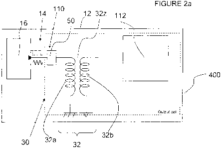
Referring to FIG. 2a, a non-differential embodiment of apparatus 30 for high-
speed output has a MIMICE 32 interposed between pad 112 and an output signal
path
SUBSTITUTE SHEET (RULE 26)
CA 02687120 2009-11-06
WO 2008/134889 18 PCT/CA2008/000861
110 having at least one signal converter 50 for transforming signal 14. Signal
converter
50 may comprise a simple element such as a buffer or a more complex element
such as a
continuous carrier RF modulator or preferentially an ultra wide band pulse
generator. For
non-limiting purposes of illustration, all figures, this description, and the
following
descriptions of the present device use a nominal equivalent of a transformer
or coupled
inductors to illustrate MIMICE 32. To those skilled in the art, it will be
apparent that
MIMICE 32 can be a significantly less complex combination of the constituent
components integrated to provide high efficiency coupling and a high level of
ESD
protection while being small and using minimal power. Furthermore, while the
embodiments discussed below and illustrated in the corresponding figures show
an
inductor, this is only illustrative of the concept. The actual coupling
achieved by the
MIMICE 32 devices may be a complex interaction of electromagnetic capacitive
and
inductive coupling. This is demonstrably different than the `proximity'
capacitive
coupling.
Shown with MIMICE 32 are connections to grounds shown as two different
symbols. With a MIMICE 32 structure having dielectric isolation, it is
possible for the
elements to be connected to different grounds and operate at different
potentials. This
enables both signalling level differences and enhanced signal return paths.
With some
embodiments the grounds are shared, in others they are separated, in yet
others they are
tied with impedances to reduce deleterious effects of ground currents. The
MIMICE 32
structure gives an additional design freedom dimension not available for
strictly wired or
strictly dielectric isolated methods.
Referring to FIG. 2b, high-speed signal output apparatus 30 has a differential
embodiment of MIMICE 32 and two pads 112a, 112b. Signal converter 50 drives
the
MIMICE 32 differentially. For example, using a"H-Bridge". Driving the MIMICE
32
differentially has several benefits including improved voltage swing,
efficient power
transmission transmit and improved common mode rejection at the receiver when
compared to single ended configurations. Alternatively, referring to FIG. 2c,
the
inductive component at the output signal path 110 side of MIMICE 32 may be
connected
SUBSTITUTE SHEET (RULE 26)
CA 02687120 2009-11-06
WO 2008/134889 19 PCT/CA2008/000861
to the circuit's common signal return path. For example, Vss or Ground which
may also
include one or more connections to the substrate.
Referring to FIGS. 3a through 3c, a high speed input cell apparatus 130
comprises
at least one pad 112 at which a signal is received, MIMICE 32 and an input
signal path
114. Pad 112 is electrically coupled to first half cell 32a of MIMICE 32 and
thus a signal
present at pad 112 is preferentially coupled electromagnetically to the
juxtaposed second
half-cell 32b of MIMICE 32. Second half-cell 32b of MIMICE 32 is electrically
coupled
to input signal path 114. Input signal path 114 has a signal converter 52
(preferentially an
ultra wide band pulse receiver, or alternatively, a continuous carrier RF
demodulator))
and application specific circuit 24. When one pad 112 is electrically
connected to first
half cell 32a of MIMICE 32, input apparatus 130 is non-differential as
illustrated in FIG.
3a. When two pads 112a, 112b are electrically connected to first half cell 32a
of MIMICE
32, apparatus 130 is differential as illustrated in FIGS. 3b and 3c. FIG. 3c,
as an
example, does not include the signal converter 52, which may not be required
where the
signal is of sufficient magnitude or the application requires minimal
complexity. In
FIGS. 2a - 3b and other figures, signal converter 50 is used to represent an
"input" signal
converter, and signal converter 52 is used to represent an "output" signal
converter.
However, it will be understood that either may act as an input or output
signal converter,
or both, depending on the situation, as will be described below.
The structures and methods described herein are preferably used with a
continuous carrier wave, or with ultra-wideband (UWB) pulses. The term UWB is
generally used to describe a radio technology that can be used at very low
energy levels
for short-range high-bandwidth communications by using a large portion of the
radio
spectrum, and is defined by the FCC as a pulse with a bandwidth that exceeds
the lesser
of 500 MHz or 20% of the center frequency. UWB pulses are generally used in
applications that target sensor data collection, precision locating and
tracking
applications. In the devices described herein, UWB pulses are used for ultra
short range
communications. In other words, the UWB pulses are used to transmit data
locally, i.e.,
much less than the wavelength of the principal pulses for the coupled
connection.
SUBSTITUTE SHEET (RULE 26)
CA 02687120 2009-11-06
WO 2008/134889 20 PCT/CA2008/000861
The continuous carrier wave is an RF signal. Preferably, a higher frequency is
used to allow for a higher data rate as well as a more efficient coupling,
such as a
frequency of 500 MHz or greater, or more preferably, a frequency of 1 GHz or
greater.
The continuous carrier wave may be modulated using any of the known modulation
techniques which are practical to implement in a chip as described herein, as
will be
recognized by those skilled in the art.
The RF signal or the UWB pulses are produced by a coupling device that
generates a signal in the transmitting half-cell in a MIMICE 32 to cause the
two half-cells
to become electromagnetically coupled and therefore transmit information
across the
dielectric barrier separating them. The coupling device may be a signal
converter, such as
a digital to UWB pulse converter, a modulator, or other device that performs
similar
functions, depending on the type of signal transmitted or modulation technique
used. The
receiving half-cell where the signal is received will also have a demodulator,
or a signal
converter to reconstruct the signal. Preferably, the half-cells will have a
coupling
coefficient of about 0.1 or greater, or more preferably, about 0.3 or greater.
If, however,
the coupling coefficient is lower, for example around 0.01, techniques may be
used in the
art to increase the signal strength, sucli as by using a low noise am.plifier.
Referring to FIG. 4, another embodiment of MIMICE 32 apparatus 30 represents
a method for providing DC restoration in a MIMICE 32 system. In an
illustrative
example, a resistor 34 has a large resistance, for example 100,000 ohms or
higher, which
provides DC restoration or DC information to both sides of MIMICE 32 while
having a
sufficiently large value of resistance to have a minimal negative effect on
the protection
against ESD and other damaging conditions inherent in the protection afforded
by the
MIMICE 32 concept.
The MIMICE 32 structure and method provides a mechanism to which additional
shielding and protection beneficially may be added without compromising the
benefits of
the fundamental concept and MIMICE 32 architecture. The following examples
illustrate
SUBSTITUTE SHEET (RULE 26)
CA 02687120 2009-11-06
WO 2008/134889 21 PCT/CA2008/000861
options for adding a shield component to the MIMICE 32 system. In FIGS. 2a
through
3c, no shield is present. In FIGS. 5a and 5b, MIMICE 32 architecture includes
a shield 36
for protection against unwanted signals and a means to increase the dielectric
separation
while minimizing the coupling loss between the input and output ports of
MIMICE 32.
The working structure can include means for input, output, or a combination of
input and
output. Optionally, the structure of MIMICE 32 may include a ground, a
floating ground,
or other protective connections, of which FIGS. 5a and 5b show examples of
options
available.
Referring to FIG. 5a, one option is to include a metal shield 36 between the
first
half cell 32a and second half cell 32b of MIMICE 32, thereby improving
shielding. As in
FIG. 2a, the MIMICE 32 device is shown with two different ground connections
which
may be configured as one common ground or separate depending on desired ground
return conditions. The metal shield is not grounded.
Referring to FIG. 5b, each of first MIMICE 32 half cell 32a, second MIMICE 32,
half cell 32b and metal shield 36 are grounded, thus forming a buffered
electrostatic
discharge protector. It will be recognized that similar protective measures
can be taken by
including metal shield 36 in MIMICE 32 of high-speed input apparatus 130 (not
illustrated). In this figure, a third grounding connection is shown for the
shield. This
connection maybe alternatively be left unconnected as in FIG. 5a or connected
in
common with another ground or connected to either of the half cell grounds.
Referring to FIG. 6a, additional protection against ESD may be provided using
prior art device 20a, where device 20a for ESD protection typically is smaller
than is
required for protection of prior art devices as illustrated in FIGS. la and
lb. An example
would be to have protective ESD of 1/10 or 1/100 of the prior art combined
with
MIMICE 32 to give exceptional protection at the same time as being very high
speed and
very low power. It will be recognized that similar devices to 20a can also be
included in
the high-speed output apparatus 30 (not illustrated) in MIMICE 32.
SUBSTITUTE SHEET (RULE 26)
CA 02687120 2009-11-06
WO 2008/134889 22 PCT/CA2008/000861
Referring to FIGS. 2a through 6a, pads 112, 112a, and 112b provide capability
for
connections to other circuits or devices on the same integrated circuit or on
the same
substrate or on other substrates as will be described later with reference to
FIGS. 11a
through 1 I e.
Referring to FIG. 6b, two separate integrated circuit bodies 400 each
containing
internal electronic circuits 16a and 16b for both transmitting (e.g., circuit
16a) and
receiving (e.g., circuit 16b), signal converter 50, signal converter 52,
MIMICE half cell
output 32a and coupling 32b, MIMICE half cell input 32b' and coupling 32a',
signal 14d,
to be transmitted, signal 14e in the middle of the coupler 84, data output
14f, and a
separable coupler 84 with half cells at each end. This figure shows how to
connect two
chips with a complete intercommunications system. Note that ESD structures are
not
required to obtain high speed communications. Also shown are representative
input
signals 14d, signals 14e in the middle of the coupler 84, and output signals
14f. These
signals, which were obtained by simulation, show that the device is able to
support very
high speed communication. In the simulation, a 1 GHz data signal is used.
Examination of
the middle signal shows that there is very high capacity in the signal (in
this case a data
transfer capacity) on the order of 500% of the represented 1 GHz signals. This
experimentation shows the large data capacity of this device without the need
of a RF
carrier or other such power consuming or complicated system used by prior art
implementations.
Referring to FIG. 7a through 7g, bi-directional conununications within or
between
integrated circuit bodies 400 may be accomplished using apparatus 230 having
MIMICE
32.
Referring to FIG. 7a, apparatus 230 has both signal output path 110 and signal
input path 114 coupled to first half-cell 32a of MIMICE 32. Signal 14 output
from
application specific circuit 16 is coupled via output signal path 110 to
MIMICE 32 thence
to pad 112. Output signal path 110 comprises an application specific circuit
16 for
transmission of output signal 14 and signal converter 50 (preferentially an
ultra wide
SUBSTITUTE SHEET (RULE 26)
CA 02687120 2009-11-06
WO 2008/134889 23 PCT/CA2008/000861
band pulse generator, or alternatively, a continuous carrier RF modulator).
Output signal
14 originates from first circuit 16 and transfornned by signal converter 50.
The output of
the signal converter 50 is electrically coupled to first hali cell 32a of
MIMICE 32 and
thus coupled electromagnetically to the juxtaposed second half-cell 32b of
MIMICE 32.
Second half-cell 32b of MIMICE 32 is electrically coupled to pad 112 as in
FIG. 7a or to
pads 112a and 112b as in FIG. 7c. A signal incoming at pad 112 is transmitted
via
MIMICE 32 and input signal path 114 to application specific circuit 24 Pad 112
is
electrically coupled to second half cell 32b of MIMICE 32 and thus a signal
present at
pad 112 is preferentially coupled electromagnetically to the juxtaposed first
half-cell 32a
of MIMICE 32. First half-cell 32a of MIMICE 32 is electrically coupled to
input signal
path 114. Input signal path 114 has a signal converter 52 (preferentially an
ultra wide
band pulse receiver, or alternatively, a continuous carrier RF demodulator),
and
application specific circuit 24. When one pad 112 is electrically connected to
second half
cell 32b of MIMICE 32, input apparatus 230 is non-differential as illustrated
in FIG. 7a.
When two pads 112a, 112b are electrically connected to second half cell 32b of
MIMICE
32, apparatus 230 is differential as il_lustrated in FIG. 7c.
Referring to FIG. 7e, for duplex simultaneous bi-directional communications
using apparatus 230 has both signal output path 110 and signal input path 114
coupled to
first half-cell 32a of MIMICE 32. Signal 14 is coupled via output signal path
110 to
MIMICE 32 thence to pad 112. Output signal path 110 comprises an application
specific
circuit 16 for transmission of output signal 14 and signal converter 50
(preferentially an
ultra wide band pulse generator, or alternatively, a continuous carrier RF
modulator).
Output signal 14 originates from first circuit 16 and transformed by signal
converter 50.
The output of the signal converter 50 is electrically coupled to first half-
cell 32a of
MIMICE 32 and thus coupled electromagnetically to the juxtaposed second half-
cell 32b
of MIMICE 32. Second half-cell 32b of MIMICE 32 is electrically coupled to pad
112 as
in FIG. 7e or to pads 112a and 112b. A signal incoming at pad 112 is
transmitted via
MIMICE 32 and input signal path 114 to application specific circuit 24. Pad
112 is
electrically coupled to second half cell 32b of MIMICE 32 and thus a signal
present at
pad 112 is preferentially coupled electromagnetically to the juxtaposed first
half-cell 32a
SUBSTITUTE SHEET (RULE 26)
CA 02687120 2009-11-06
WO 2008/134889 PCT/CA2008/000861
24
of MIMICE 32. First half-cell 32a of MIMICE 32 is electrically coupled to
input signal
path 114. Referring to FIG. 7d and 7f, the input signal path has a signal
converter 52
(preferentially an ultra wide band pulse receiver, or altematively, a
continuous carrier RF
demodulator), a signal processing element 28a and application specific circuit
24. An
image 14a of signal 14 is electrically coupled to signal processing element
28a. Signal
processing element 28a applies a transform to the input signal path. Signal
processing
element 28a preferentially performs a subtract function but could perform
other
mathematical or signal processing functions. In the preferred embodiment,
signal
processing element 28a subtracts image 14a from receive signal 14b thus
enabling
application specific circuit 24 to receive only incoming signals to pad 112
and to ignore
the near end transmitted signals 14. The output of signal processing element
28a is
electrically coupled to application specific circuit 24. When one pad 112 is
electrically
connected to second half cell 32b of MIMICE 32, input apparatus 230 is non-
differential
as illustrated in FIG. 7d. When two pads 112a, 112b are electrically connected
to second
half cell 32b of MIMICE 32, apparatus 230 is differential as illustrated in
FIG. 7f. In this
manner, a fall duplex communication can be carried out simultaneously in both
directions
over MIMICE 32. This enables simultaneous bi-directional communications over a
single
wire or a pair of wires while maintaining the other advantages of the MIMICE
32 that is
protection, high speed, and small size and reduced power consumption.
Apparatus
illustrated in other FIGS. 7a-c, 7e, 7g can be used in a manner which is input
or output or
time switched between each side.
Refemng to FIGS. 7c and 7e, apparatus 230 has two pads 112a, 112b and so is a
differential I/O cell, whereas apparatus 230 as illustrated in FIGS. 7a, 7b
and 7d is a non-
differential I/O cell. These figures show different implementations of single
ended double
ended, differential, non-differential, and bi-directional methods of
instantiating MIMICE
32. Each may have an advantage that is one or more of size or speed or
applicability to
the specific application. For example, some technologies are easier to
implement in single
ended architectures than others, differential systems are capable higher speed
but use two
wires for each signal, etc. These examples show the flexibility of MIMICE 32
in different
apparatus and applications.
SUBSTITUTE SHEET (RULE 26)
CA 02687120 2009-11-06
WO 2008/134889 25 PCT/CA2008/000861
Referring to FIG. 8a, a device 120 may be in communication with a plurality of
5. other devices 120(x), where x is a number from 1 to n, via wire links 54.
Device 120 has
a transmission circuit 56 and a receiving circuit 58. Transmitting circuit 56
at device 120
is wired via one branched link 54 to receiving circuits 58 at each of other
devices 120(x).
Similarly, receiving circuit 56 at device 120 receives signals transmitted
from
transmitting circuits 56 at each of other devices 120(x). Transmission
circuits 56 and
receiving circuits 58 may be integrated into device 120 or may be separate
chips. It will
be understood that teachings herein can be applied to a variety of packages
and devices
not limited to a single a package or package type. For example, device 120 and
device
120(x) may be, without limitation, a monolithic integrated circuit, a multi-
chip module,
or system in package component, a printed circuit card, chip, substrate, PCB,
MEMS
device, etc., or a combination of these. Transmission circuits 56 and
receiving circuits 58
ca_n be unidirectional or bi-directional, one of differential or single ended
pad signalling.
Circuits 56 and 58 incorporate the full cells or half-cells that make up
MIMICE 32 in
accordance with the teachings contained herein.
Referring to FIG. 8b, when each of a set of devices 120 has bi-directional
communication capability provided by apparatus 230 installed at elements 56,
58,
communication between a plurality of said devices 120 can be in bi-directional
and full
duplex mode via wire links 54. In FIG. 8b element 120 can be any of a chip,
substrate,
PCB, MEMS device, etc. and element 61 can be any of unidirectional or bi-
directional
differential cells as discussed previously. Chips 56 and 58 are both included
in each
element 61 in accordance with the teachings contained herein, such that each
element 61
also includes MIMICE 32.
Referring to FIG. 8c shows how a device comprising several MIMICE 32,
included in element 61 as described above, can enable devices to communicate
along a
single differential pair. This allows extended application including use over
extended
SUBSTITUTE SHEET (RULE 26)
CA 02687120 2009-11-06
WO 2008/134889 26 PCT/CA2008/000861
distances and at different nodes. This may be a distributed or so-called bus
form of
communication between, for example, processing units or one of many
applications for
such a device. The loop connection topology shown allows more than one
apparatus to
communicate via interconnection and use a variety of known techniques for
signal
stabilization and timing. Each device can be centrally or individually timed
and several
techniques in that art can be used to compensate for greater or lesser
distances and signal
states. MIMICE 32 in this case allows a distributed high speed system to be
created
without the burden of needing ESD protection at each node. Other techniques
would
require extensive ESD and buffering which would have to be additionally
compensated
for. Such compensation requires greater power and introduces impairments which
must
be further compensated, thus the MIMICE 32 doubly benefits applications and
implementations.
FIGS. 9a and 10 illustrate construction side views of MIMICE 32 that may be
incorporated into apparatus 30, apparatus 130 and apparatus 230, examples of
which will
now be described. FIG. 10 also shows a stacked double insulated MIMICE 32. The
ground connection may be grounded, floating, or tied to ESD protection to
maximize
speed protection or other parameter. FIG. 10 also shows the monolithic nature
of the
MIMICE 32 constnzction into a monolithic body A 00. It will be understood from
FIG. 10
that one or more of the half cells 32a and 32b may be recessed from the face
of the
electronic device it is associated with that is adjacent the other electronic
device and that
it is in communication with. The term "recessed" is used to describe the half-
cell being
embedded in the electronic device, or positioned within a cavity, such as if
the half cell
were monolithically formed. While the half-cell is recessed, the outer surface
may still
be flush with the face of the electronic device due to the height of the half-
cell. The half-
cell may also be embedded by placing a layer of solid dielectric material over
the half-
cell.
One should note the preferred embodiment of MIMICE 32 has planar, quasi two
dimensional structures which are compatible with IC fabrication and not
separate and
SUBSTITUTE SHEET (RULE 26)
CA 02687120 2009-11-06
WO 2008/134889 27 PCT/CA2008/000861
disparate component construction of coils, capacitors, windings, cores,
interconnects of
prior art communications interconnection techniques.
Illustrations of the layered architecture on chip 12 having one or more of 1/0
apparatus 30, 130, 230 are shown in FIGS. 9a. Referring to FIG. 9a, chip 12
comprises a
base 72 onto which are bonded a plurality of layers 74. Active electrical
components and
electrical insulators situated in layers 74 are the working components of chip
12. Chip 12
is supported on a substrate 82. In this illustration, a first half-cell 76 and
a second half-
cell 78a are shown. It can be seen from this illustration that it is possible
to position
elements of the integrated circuit below the half-cells 76 and 78a as shown.
This may be
advantageous, for example, when the half-cells 76 and 78a are inductors, which
may take
up a relatively large amount of area on the chip 12.
FIG. 9a also illustrates that the active circuits 74a can be placed under the
MIMICE and connection elements 76, 78a, 78b, 112. This is a key feature in
that the
structures can be thus made very small completely under the MIMICE structure.
In this
illustration, elements, such as pad 112, can be recessed into a non-
interfering manner
protecting against electrical contact with elements 76 and 78a, and embedded
within the
structure 12. This provides galvanic isolation to external elements and
struct~.zres or
subsequent MIMICE additional structures, such as element 78b.
As first half-cel176 and second half-cel178a are parallel to and closely
adjacent or
juxtaposed to each other, there are strong communications between them. When
electrical
components are in stacked layers 74 of chip 12, the demand for surface area is
reduced to
devices where all components are in one or more layers. Among the other
components is
a conductive pad 112, usually metal. In the present application, metal pad 112
and first
half-cell 76 are in electrical communication when they both are components of
an input
apparatus, output apparatus, or input/output apparatus, as illustrated in
FIGS. 2a through
7g. Alternatively, metal pad 112 may serve for attachment of hardwired
connections to
other chips or electrical components that are mounted on the same substrate 82
as chip
12.
SUBSTITUTE SHEET (RULE 26)
CA 02687120 2009-11-06
WO 2008/134889 28 PCT/CA2008/000861
Referring to FIG. 9b, because of the small size and low power of the
illustrated
design, multiple MIMICE 32 cells can be placed on a single monolithic IC
without the
higher heat generation and power supply limitations that inhibit applications
of prior art
technologies and techniques. The principles discussed herein enable massively
parallel
operation without wasting energy on driving protection capacitance or other
circuits. The
principles enable preferential impedance matching, which also adds to the
energy
efficiency compared to of that of the prior art.
Referring to FIG. 10, in one example an input structure and an output
structure of
one of output apparatus 30, input apparatus 130 or input/output apparatus 230
are
separated by a dielectric layer or layers 32z. In a second example, two extra
layers are
interposed between the input layer and the output: a shield structure 36 and
an additional
layer of dielectric 32z to ensure that the respective components of the
circuitry and shield
36 are electrically insulated from one another. While in this illustrative
example the
shield is grounded, it could be connected to other structures as required. The
MIMICE
32 structure shown as "coupled inductors" is comprised of two half-cell
elements 32a,
32b containing inductive, capacitive and conductive elements monolithically
built into
the IC body 400. One of the hall=cells connects to the internal chip circuitry
and the other
half-cell connects to pads external to the IC body 400. Thus, internal active
electronics in
either package associated with the half-cells are not directly exposed to
external I/O
signals or stresses. As will be discussed below, this design enables two
packages to be
separated by distances 32d while still communicating in a protected, high
speed and
efficient manner. The dielectric isolation 32z supports isolation and
protection while the
coupling of the two half-cells 32a, 32b is designed to be preferential for
high speed
signalling purposes. In addition, the dielectric isolation of separation
distance 32d also
increases isolation and protection. The MIMICE 32 could be built in a non-
monolithic
manner should the application warrant it. The discussion with respect to the
device being
monolithic is a preferred embodiment, but other designs will also be apparent
to those
skilled in the art and based on the discussion herein. Applications where the
two half cells
are separated for testing is one such additional application.
SUBSTITUTE SHEET (RULE 26)
CA 02687120 2009-11-06
WO 2008/134889 29 PCT/CA2008/000861
Referring to FIGS. 11 a through 11 g, pad 112 may be in electrical
communication
with other electronic components via connections 84, with connections 84
selected from
among hardwire connections and communication links via a MIMICE or half-cell
(not
illustrated) at pad 112. For example, when pad 112 on chip 12 is attached to a
substrate
82 such as a laminate printed circuit board, it is in communication with other
chips on
that same substrate. Substrate 82 may be one of a mono or multilayer laminate
material,
silicon material, ceramic material, polyamid material, or other rigid or
flexible material
that is used to support and interconnect electronic circuits. The figures
illustrate non
limiting examples of microelectronic packages such as chip-on-board, chip-on-
package,
package-on-package, package-on-board, system-in-package and integrated passive
device.
Similar or different embodiments of apparatus 30, 130 or 230 may be mounted on
separate chips 12 that are in communication. For example, a first chip 56 and
a second
chip 58 can be mounted on the same substrate as illustrated in FIGS. lla and
llb.
Alternatively, the architecture may be flip chip or chip-on-chip (FIG. 11 c).
Referring to FIG. 11 a, each of first chip 56 and second chip 58 has at least
one
pad 112. Substrate 82 has at least two pads 112 interconnected by wired
connection 84
for transmission of electrical signals. Each pad 112 on one of chips 56, 58 is
wire bonded
86 to one of pads 112 on substrate 82, thereby interconnecting first chip 56
and second
chip 58. Alternatively, wirebond 86 may be connected directly from pad 112 on
chip 56
to pad 112 on chip 58 thereby bypassing wired connection 84 on substrate 82.
Referring to FIG. 1 lb, pads 112 of the chip-on-chip combination are similarly
in
communication via wire bonds 86. In this illustrative example, first chip 56
and second
chip 58 are electrically connected to connections 92 embedded in substrate 82
that are
themselves electrically connected to wired connection 84.
SUBSTITUTE SHEET (RULE 26)
CA 02687120 2009-11-06
WO 2008/134889 30 PCT/CA2008/000861
Referring to FIGS. 11 c and 11 d, when one or both of first chip 56 and second
chip
58 are in "flip chip" orientation relative to substrate 82, each flip chip 56,
58 has at least
one solder ball or post 88. FIG. llc illustrates chips 56, 58 in communication
with
electrical connectors 80 mounted on substrate 82. Alternatively, electrical
connector 80
may be a package, socket, interposer or other space transformer. FIG. 1ld
shows chips
56, 58 in direct communication by way of pads 112 mounted on substrate 82
interconnected by wired connection 84. Electrical connection to pad 112 on
substrate 82
is achieved by conductive contact between pad 112 and solder ball or post 88.
Note
additional contacts between substrate 82 and chips 56 and 58 have been
intentionally
omitted from FIG. 11 d for clarity.
Referring to FIG. l 1 e, either or both of first chip 56 and second chip 58
may have
a first half-cell 90 for transmission/reception of signals. Substrate 82 has a
matching
second half-cell 92 interconnected by wired connection 84. A signal
transmitted from
first chip 56 via first half cell 90 adjacent said first chip 56, is coupled
to the
corresponding second half cell 92, transmitted along wired interconnection 84
to second
half cell 92 adjacent second chip 56, from which it is coupled to first half
cell 90 on
second chip or device 58. As illustrated in FIG. 12a, it is preferred that
second half cell
92 and wired interconnection 84 are embedded in substrate 82, however
interconnection
84 may be formed on or mounted to the surface of substrate 82. Alternatively,
first chip
56 or second chip 58 or both in combination may be flip chip mounted using
solder balls.
Such technique would introduce a separation between the chips 56 and 58 and
the
substrate 82 thereby introducing another dielectric barrier (preferably air
but could be
another gas or solid or evacuated and sealed in a vacuum) between first half
cell 90 and
second half cell 92.
Referring to FIG. 11 f, pad 112 is in electrical communication with other
electronic components via wired connections such that chips 56 and 58 can be
at large
distance from each other such as packaged chips on a printed circuit board or
packaged
chips on separate printed circuit boards. Herein the MIMICE 32 devices allow
isolation
between chips and enhanced com_munications. In this case, with a MIMICE 32 at
each
SUBSTITUTE SHEET (RULE 26)
CA 02687120 2009-11-06
WO 2008/134889 31 PCT/CA2008/000861
end of the wired communications link, there are two isolation protection
barriers between
the chips. This allows each end to float at a different potential with respect
to the other
and further allowing each chip to be operated at different power supply
voltage levels.
This can be done over long distances such as wired or coaxial or transmission
line
connections. This double isolation provides protection from contention which
would
normally inhibit or limit communications in other systems. In this example the
two chips
could be on different cards and communicating over a conductive backplane or
ribbon
cable.
Referring to FIG. 1 lg, electrical communication with other electronic
components
via internal connections in this illustration such that internals transmitter
and receiver
functions 56 and 58 can be at large distances or separate functions within a
single IC
body 400. Herein the MIMICE 32, and half cells 32a, devices allow isolation
between
chips and enhanced communications. In this case, with a MIMICE 32 at each end
of the
internally wired communications link 84, there are isolation protection
barriers between
the functions within the one IC. This allows each end and the middle
communications
wires each to be operated at different voltages and thus be immune to
interference from
each to each other.
FIG. 12a is an illustrative example of using interstitial element 320, in
place of
element 32 in other figures, for enhanced coupling and/or extended protection.
FIG. 12a
shows a method of creating multi-layer separation between the input and the
output for
extended ESD protection using interstitial element comprising two half cells
320a 320b
between primary and secondary elements 32a and 32b of the MIMICE 32 structure.
Half
cells 320a and 320b may be on a separate chip or substrate than half cells 32a
and 32b.
Alternatively, half cells 320a and 320b may be located on the same chip body
as half
cells 32a and 32b.
The advantage of this architecture is that it provides enhanced protection by
100%
over that of a single element (comprising two half cells 32a 32b) by using two
dielectric
interfaces 32z instead of only one illustrated in FIG. 2a. The extra
interstitial elements
SUBSTITUTE SHEET (RULE 26)
CA 02687120 2009-11-06
WO 2008/134889 32 PCT/CA2008/000861
320a, 320b in between can be designed as needed to isolate the input and
output signals.
Optionally interstitial cells or half-cells can be used on multiple mask
layers for extended
isolation. Multiple MIMICE can be connected in series to increase the
dielectric isolation
and ESD protection level, without the need for active ESD structures. Further,
MIMICE
can be stacked vertically or placed laterally or a combination of stacking and
lateral
placement.
The interstitial cell also allows for further impedance matching to optimally
match internal signals to external signals. For example if an output buffer
has a 5-ohm
impedance and the external link requires 100 ohms for perfect impedance
matching, a
5:100 or 1:20 transformation is needed. It is advantageous to use this form of
MIMICE
32 to allow two impedance transformations, one between half cells 32a and 320a
and a
second between half cells 320b and 32b. An exainple would be 1:4 and 1:5
coupling
ratios giving a total impedance transformation of 1:(4x5) or 1:20, providing
ideal
impedance matching. Optionally the center couple half cells 320a and 320b can
be
connected to ground or other protection surge protection circuit to provide
additional
protection of IC internal circuitry.
For example, in FIG. 11e, which is an example implementation of FIG. 12a, it
is
preferred that a signal transmitted via first half-cell 90 and second half-
cell 92 is a signal
which uses a small amount of energy. A micro-pulse signal is an illustrative
one which
can be used with a MIMICE 32 device. A greater amount of energy is used when a
broader signal is transmitted, and so there is a greater amount of heat
generated in first
application specific circuit 16 and pad 112, and all electrical
interconnections between
them. Wben signal 14 (in FIGS. 7a to 7f) is a micro-pulse signal, there is
considerably
less energy consumed and less heat generated. It will be recognized that
different micro-
pulse signals 14 can travel in opposite directions along all lines of
communication,
allowing full duplexing.
FIG. 12b shows how the half cells can be enhanced by the use of an
interstitial
device to enhance signal quality or provide further protection. In this
figure, element 330
SUBSTITUTE SHEET (RULE 26)
CA 02687120 2009-11-06
WO 2008/134889 33 PCT/CA2008/000861
may consist of active or passive elements which can further enhance signals.
One
example would be to have element 330 as a repeater of signals entering the
edge elements
32a. An exarnple of passive elements would be monolithic inductive and
capacitive
elements to perform filtering to enhance desired signals and reduce unwanted
ones.
Those skilled in the art would find this aspect of great utility for many of
the conditions
found in real world applications. Element 330 can be used for improved
extended
isolation/protection using passive or semi-active devices such as semi-
conductor clamps
which have low impact on the desired signals.
Because of the enhanced communication possible with a MIMICE 32 device it is
possible to envision applications in several areas. One example it to use a
MIMICE 32
interface for the production and testing of ICs where the MIMICE 32 devices
are used
further after testing for interconnect of high speed signals. In this way the
MIMICE 32
devices can be used for intentional access and later communications without
the need for
separate communications channels. This is illustrated in FIG. 13a where the
half cell of a
MIMICE 32 is used for on-chip or on-wafer testing and later for chip-to-chip
communications by the addition of different half cells which terminate for
different
purposes.
FIG. 13a shows a package 520 for an IC 501 with external connections 522 and
internal package connections 521. Also shown is open cavity 520a in the
package 520
which is a standard technique often used to enable internal connections such
as
wirebonding to be placed between the IC and its external connections. In this
illustration
wirebonding is not shown as it is a well known technique. What is shown is
that the
MIMICE 32 technique can be used with other packaging techniques, for example,
a lead
frame or ceramic carrier. In this case the internal connections are shown as
flip chip
solder balls or thermo-compression interconnects 521. In this illustration the
half cells
32a of the MIMICE 32 device are exposed. In this case they are available for
access and
communications for testing of the packaged device before encapsulation, final
lidding or
glob top. Providing access to a packaged device for testing and communications
is a
SUBSTITUTE SHEET (RULE 26)
CA 02687120 2009-11-06
WO 2008/134889 34 PCT/CA2008/000861
benefit to the MIMICE 32 technique. The full cell can be completed temporarily
for
testing or permanently for communications to other devices.
FIG. 13b shows how the separable half cell MIMICE can be used for testing and
communicating to devices 501 in wafer form 500. Device 501 is an individual IC
location
on a wafer 500 while the half cell air gap is 32z is shown between the 320c
half cell
which is connected to coinmunications or test equipment 510. In this
application of
MIMICE 32 devices they are used in the earliest stages of fabrication testing
and
assembly for partially or fully fabricated wafers and devices. One should note
that there
are several techniques known in the art to allow the separation of 32z to be
made
arbitrarily small such that the performance can be virtually the same as that
of a
monolithic device including temporary dielectrics applied only for period of
testing. One
should note that silicon wafer is an example for illustrative purposes, and
that other
devices such as assemblies or panels of devices can be used in a similar
manner. Panels
of ICs on laminates or frames are an example that can utilize the MIMICE 32
concept.
Also while FIG. 13b shows a single headed device it will be recognized that
the same
application can be performed in a parallel or multiplex manner, thereby
enabling parallel
communications or testing to be performed.
FIG. 13c shows a packaged 520 IC 501 with no lid installed and into which a
half
cell MIMICE 32 device 320c is inserted for testing. This is an illustration
showing how a
MIMICE 32 device can be used for testing devices mounted in packaged ICs. The
test
equipment or testers 510 are interfaced thru a half cell 32b to the IC 501
half cell 32a.
Also shown are internal and external electrical package connections 521 522
shown as
solder balls in this illustration. The benefits of isolation combined with
high speed
communications are useful in this illustrated application of the MIMICE 32
concept.
FIG. 13d shows two ICs interconnected with a MIMICE 32 interface 320
enabling chip to chip communications. In this case after testing it is
possible to use the
same interface which was used for testing for chip to chip communications. The
top
illustration shows a cross section of the packaged ICs 520 and their internal
ICs 501 and
SUBSTITUTE SHEET (RULE 26)
CA 02687120 2009-11-06
WO 2008/134889 35 PCT/CA2008/000861
the isolation/dielectric gap or barrier 32z forming MIMICE 32 interconnect 320
between
the two ICs. The lower illustration shows a finished packaged two chip system.
One of
several well known fabrication techniques can be used to seal the system as
required by
the application. Glob top or vacuum backfill are two techniques known in the
industry. In
this way a multiple internal chip solution can be aggregated together using
MIMICE 32
methods to create greater performance and utility. One example would be to
have a
microprocessor chip connected with MIMICE 32 apparatus to a memory chip. The
high
speed and low power of the MIMICE 32 technology would enable multiple
advantages to
such products and systems.
FIG. 13e is an illustration showing how two devices 501 of a different
packaging
technique can be connected with MIMICE 32 devices. In this application of
MIMICE 32
technology the devices 501 are bare dies which are flip chip bonded to a
carrier or
substrate 530. In this case the MIMICE 32 half cells 32a are fabricated on the
bare IC 501
and flipped and bonded to a substrate by in the illustrative exainple micro
solder balls or
posts 521. Very high density packaging can be obtained in this way and the
MIMICE 32
can be used for chip to chip communications as illustrated in this FIG. 13e.
In this case
the MIMICE 32 interconnect 32b is shown as part of or constructed on the
substrate 530.
The half cells 32a 32b and dielectric gap 32z are sh own in the illustration
detail, which is
not to scale. The dielectric gap as discussed above can be constructed out of
various
dielectric materials and controlled with micro-fabrication techniques.
Multiple dies can
be placed with high density using this technique and MIMICE 32 technology
enables
close communications between devices which would be otherwise restricted by
space,
speed and power consumption considerations.
FIG. 13f shows multiple ICs 501s interconnected with multiple MIMICE 320 and
32. This illustration shows a plan view of four chips or ICs in a full
interconnected
topology for applications such as a System In Package (SIP) or a
multiprocessor system.
Also shown is package outline 501 a showing the potential of this technique to
create
systems in a package. Not shown are either external signal connections or
final package
fill for which there are well known techniques and solutions.
SUBSTITUTE SHEET (RULE 26)
CA 02687120 2009-11-06
WO 2008/134889 36 PCT/CA2008/000861
In this illustration each IC 501 can communicate with each other IC via a
direct
MIMICE 32 enabled communications path. The benefits of low power and high
speed
manifest themselves in multiple ways for multichip systems, not the least of
which is
power requirements which would otherwise limit multiple chip designs. The
power
savings described earlier by not having to support ESD structures etc. allow a
system like
that illustrated to grow beyond the previous limits. With these teachings, one
skilled in
the art will envision other applications including multiple systems designs
with high
speed microprocessors memory etc. combined into one system.
FIG. 13g shows how MIMICE 32 structures can be embedded into substrates to
facilitate communications between two or more integrated circuits. In this
case is an
illustration showing how MIMICE 32 devices can be configured to be embedded
into a
substrate to enable communications between assemblies of ICs. Several known
substrate
techniques can accommodate MIMICE 32 and enhancements as outlined in FIG. 12b
element 330. Substrate techniques such as Printed Circuit Boards (PCB),
Multichip
Modules (MCM), ceramic substrates, Passive Integrated Circuit Substrates
(PICS),
Redistribution Chip/Circuit Packaging (RCP) etc. are techniques and
applications of the
MIMICE 32 teclmique and apparabus. In FIG. i3g, elements of FIG. 13e (32b,
320,530)
are integrated into the substrate 530a which can be done using several well
known
techniques.
Several advantages accrue from each embodiment of the MIMICE 32 apparatus
as shown in the above by way of example apparatus 30, apparatus 130, and
apparatus 230
when compared with the standard approaches exemplified by apparatus 10.
Prior art and standard practice apparatus 10:
= has a high capacitance,
= requires high power to amplify and transmit signal 14,
= has low speed of transmission of signal 14,
= causes delay in transmission of signal 14, and
= the sum of the components of apparatus 10 requires a large area.
SUBSTITUTE SHEET (RULE 26)
CA 02687120 2009-11-06
WO 2008/134889 37 PCT/CA2008/000861
In contrast, because each embodiment of apparatus 30, apparatus 130 and
apparatus 230 has no electrostatic discharge diodes, and because signal
converter 50 has
low capacitance, each of apparatus 30, apparatus 130 and apparatus 230:
= has a much lower overall capacitance than that of prior art apparatus 10,
= has much higher speed than prior art apparatus 10,
= allows very high rates of data transfer to/from pad 112,
= has a higher coupling coefficient,
= requires far less power to transmit signal 14 to/from pad 112, and so
= produces far less heat than prior art apparatus 10,
= has a low requirement for area,
= enables transmission/reception of signals having a wide range of
frequencies, and
in particular has better capability to transmit/receive high frequency signals
when
compared to prior art apparatus 10,
= galvanic isolation between circuits = ability to power chips with different
power supplies or different voltages or
different ground potentials or a combination of these; and
= improved signal integrity
Another advantage is that, in contrast to some prior art which requires
particular
data transmission techniques, the devices described above can be used with
well known
standard methods such as clock and data encoding, phase locked loops or even
simple
received data tiiueshoiuing to achieve veiy high u.ata rat^cs ariu speeds.
The signal coupling in the embodiments described above is shown to be enhanced
qualitatively and quantitatively beyond the loose electromagnetic coupling
described in
the prior art to the point of enabling sufficient signals for robust data
transfer.
Furthermore, coupling is achieved by close proximity and in fact, is
monolithic in one
illustrated embodiment or near monolithic construction in another embodiment
rather
than depending on several disparate components and structures to achieve
loose, or weak,
electromagnetic coupling.
SUBSTITUTE SHEET (RULE 26)
CA 02687120 2009-11-06
38
WO 2008/134889 PCT/CA2008/000861
In one embodiment, the teachings purposely couple and create strong signals
and
strong coupling to enhance signalling capability and provide high speed
preferenced
communications for signal transfer, data transfer and any number of other
specific
applications.
Thus the above teachings can be used advantageously for more rapid
communications between integrated circuits and related circuits than can be
attained
using prior art systems. Applications include communications for serial and
parallel
needs and standards such as Ethernet controllers and microprocessors, and
between any
of combinations of field programmable gate arrays (FPGA), microprocessors,
memory
devices, digital signal processors, DRAM, etc.
The device described above is not limited in its various applications to the
details
of construction and the arrangement of components set forth in the previous
and
following description or as illustrated in the drawings. It is capable of
other embodiments
and of being practiced or of being carried out in various ways. Also, the
language and
terminology used here is for the purpose of description and should not be
regarded as
limiting. The use of "including," "compr sing," or "having," "containing",
"involving",
and variations thereof herein, is meant to encompass the items listed before
and after and
equivalents thereof as well as additional items. A reference to an element by
the indefinite
article "a" does not exclude the possibility that more than one of the element
is present,
unless the context clearly requires that there be one and only one of the
elements.
The following claims are understood to include what is specifically
illustrated and
described above, what is conceptually equivalent, and what can be obviously
substituted.
Those skilled in the art will appreciate that various adaptations and
modifications of the
described embodiments can be configured without departing from the scope of
the claims.
The illustrated embodiments have been set forth only as examples and should
not be taken
as limiting the invention. It is to be understood that, within the scope of
the following
claims, the invention may be practiced other than as specifically illustrated
and described.
SUBSTITUTE SHEET (RULE 26)