Note: Descriptions are shown in the official language in which they were submitted.
CA 02687582 2009-11-17
CRYPTOPROCESSOR WITH IMPROVED DATA PROTECTION
Field of the invention
The present invention applies to an electronic circuit
comprising a RAM in which data are stored, capable of deleting
the data on detection of an unauthorized access attempt.
Discussion Of Prior Art
Many electronic systems comprise a RAM in which
critical data necessary to the proper operation of the
electronic system and which must not be accessible to an unau-
thorized user, are stored. As an example, a card reader, for
example, a bank card reader, generally comprises an electronic
circuit, called cryptoprocessor, dedicated to the storage of
critical data and to the performing of arithmetical operations
on the critical data. The critical data for example correspond
to the personal identification numbers of the cards introduced
into the reader or to keys used by the cryptoprocessor to imple-
ment encryption algorithms. The cryptoprocessor is capable of
deleting all the critical data as soon as an attempt of unautho-
rized access to the reader is detected by security devices
equipping the reader to prevent an individual from reading to
the critical data stored in the cryptoprocessor.
The reader components, among which the cryptoproces-
sor, are generally powered from a single power source, for exam-
CA 02687582 2009-11-17
2
pie, the mains power supply, called main power supply hereafter.
A backup power supply source is generally provided at the level
of the reader to power the cryptoprocessor even when the main
power supply is interrupted so as to enable the data retention,
the operation of the security devices and the deleting of the
critical data in case an unauthorized access attempt is
detected. The backup power supply source is for example formed
of a cell connected to the cryptoprocessor and providing a
backup power supply voltage.
Due, in particular, to the structure and to the size
of the backup power supply and to current security requirements
in the field of bank card readers, the protection of the backup
power supply source requires expensive mechanical devices (for
example, a cover with an opening detector) and it is generally
not possible to fully exclude the risk for an individual to be
able to access the backup power supply source without for this
intrusion to be detected by the cryptoprocessor. According to a
first possibility, it could be envisaged to deactivate the
backup power supply source, which would result in a stopping of
the cryptoprocessor operation without for the critical data
stored in the cryptoprocessor RAM to have been deleted. Although
an interruption of the power supply of a RAM theoretically
causes the loss of the data stored therein, there is a risk for
the data to be recoverable due to persistence phenomena specific
to certain types of conventional RAMS used in readers. According
to a still less favorable assumption, one could envisage, by
varying the backup power supply voltage, to disturb the crypto-
processor operation so that an access to the cryptoprocessor
becomes possible without causing a deleting of the critical data
in the RAM, which then remains powered. The critical data might
then be read by an unauthorized person.
Document GB2195478 describes an electronic circuit
comprising a main memory, a secondary memory, and an intrusion
detector. The secondary memory is deleted on detection of an
CA 02687582 2015-06-16
3
intrusion. The electronic system is powered by an external power
supply source.
Document WO 99/40501 describes an electronic system
comprising a single memory connected to a main power supply
source and an intrusion detector. The secondary memory is
connected to another power supply source on detection of an
intrusion to be deleted.
Summary of the invention
The present invention aims at an electronic circuit
comprising a RAM in which critical data are stored, which is
capable of preventing the access to the critical data in case of
a variation of the electronic circuit power supply voltage.
Thus, an embodiment of the present invention provides
an electronic circuit made in integrated form, comprising a
first data storage RAM; a processing unit configured to perfolm
a deleting operation in the first RAM; and an access teLminal
connected to the processing unit and receiving a first power
supply signal provided by a first power supply source external
to the electronic circuit. The circuit further comprises a
second RAM in which is stored a key, said data being encrypted
by implementation of said key; and a second power supply source
integrated to the electronic circuit and configured to provide a
second power supply signal to the processing unit, the
processing unit being configured to detect that an unauthorized
access attempt is occurring based on comparison of the first and
second power supply signals and to delete said key while the
processing unit is powered by the second power supply source.
The processing unit comprises MOS transistors and the capacitive
element corresponds to the stray capacitances of the MOS
transistors. Storage capacity of the second RAM is smaller than
storage capacity of the first RAM.
According to an embodiment, the second power supply
source comprises a capacitive element connected to the access
terminal and to the processing unit, the electronic circuit
further comprising a device configured to prevent a fast
CA 02687582 2015-06-16
4
discharge of the capacitive element by an external action on the
access teiminal.
According to an embodiment, the storage capacity of
the second RAM is smaller than one thousand bits.
According to an embodiment, the circuit comprises an
additional access telminal intended to be connected to a third
power supply source, external to the electronic circuit, ensur-
ing the power supply of the processing unit in a normal operat-
ing mode of the electronic circuit, the first power supply
source ensuring the power supply of the processing unit when the
third power supply source is inactive.
According to an embodiment, the first power supply
source comprises a cell connected to the access te.minal and a
capacitor assembled in parallel across the cell.
The present invention also provides a system
comprising a package including the first power supply source and
an electronic circuit such as previously defined connected to
the first power supply source via the access terminal of the
electronic circuit.
The present invention also provides a method for
protecting data, the method comprising: storing said data in a
first RAM of an electronic circuit, storing a key in a second
RAM of the electronic circuit, wherein said data being obtained
by an encryption implementing said key, performing, by a
processing unit of the electronic circuit, a delete operation in
the first RAM, receiving, by an access telminal connected to the
processing unit, a first power supply signal delivered by a
first power supply source, exteinal to the electronic circuit,
providing a second power supply signal to the processing unit,
detecting, by the processing unit, that an unauthorized access
attempt is occurring based on comparison of the first and second
power supply signals; and deleting said key, the processing unit
being then powered by the second power supply source. The
processing unit comprises MOS transistors and the capacitive
element corresponds to stray capacitances of the MOS
CA 02687582 2015-06-16
transistors. Storage capacity of the second RAM is smaller than
storage capacity of the first RAM.
According to an embodiment, the first power supply
signal corresponds to a first voltage and the second power
5 supply signal corresponds to a second voltage, an unauthorized
access attempt being detected when the difference between the
second and first voltages is greater than a given threshold for
a given time period.
Brief Description of the Drawings
The foregoing objects, features, and advantages of the
present invention, as well as others, will be discussed in
detail in the following non-limiting description of specific
embodiments in connection with the accompanying drawings, among
which:
Fig. 1 shows a conventional example of a card reader
cryptoprocessor; and
Fig. 2 shows an embodiment of a card reader cryptopro-
cessor according to the present invention.
Detailed Description
For clarity, the same elements have been designated
with the same reference numerals in the different drawings.
A conventional example of a cryptoprocessor will now
be described in relation with Fig. 1. As an example, a crypto-
processor equipping a card reader, for example, a bank card
reader, is considered. However, the present invention may apply
to any type of cryptoprocessor.
Cryptoprocessor 10 corresponds to an integrated
circuit comprising a power supply terminal Bl to Which is
applied a main power supply voltage VDD provided, for example,
based on the mains power supply. As an example, main power
supply voltage VDD is on the order of 2 volts. Cryptoprocessor
10 comprises a microprocessor 12 (pP) which performs, in normal
operation, the conventional operations specific to cryptopro-
CA 02687582 2009-11-17
6
cessor 10. For this purpose, cryptoprocessor 10 comprises one or
several access terminals (a single terminal B2 being shown in
Fig. 1) via which microprocessor 12 exchanges data with other
components of the reader. Cryptoprocessor 10 further comprises a
RAM 14 from and into which microprocessor 12 is capable of read-
ing and writing data, especially so-called critical data. The
size of memory 14 depends on the amount of data processed by
cryptoprocessor 10 and is, conventionally, on the order of a few
kilobytes, for example, 8 kilobytes.
Cryptoprocessor 10 further comprises a security module
or automaton 16. Security module 16 is a logic circuit which has
a simpler structure than microprocessor 12 and which may
comprise from a few thousands to a few tens of thousands of
logic gates. Security module 16 may exchange data with micropro-
cessor 12 and at least perform write operations into memory 14.
Security module 16 may further exchange data with other compo-
nents of the reader via access terminals (a single terminal B3
being shown in Fig. 1). An input/output interface module 18
(PIO) is generally provided between security module 16 and
access terminal B3. As an example, security module 16 may
receive through access terminal B3 signals transmitted by secu-
rity devices equipping the reader. An example of a security
device corresponds to a circuit of lattice type comprising a
conductive track having its interruption, representative of an
unauthorized attempt to access the reader, cause the delivery of
an alarm signal to cryptoprocessor 10. Another example of a
security device corresponds to a dummy keyboard key permanently
ensuring an electric contact between two conductive tracks in
normal operation, an interruption of the contact being repre-
sentative of an unauthorized access attempt and causing the
delivery of an alarm signal to cryptoprocessor 10. Another secu-
rity device corresponds to a temperature sensor, an excessive
temperature being representative of a malfunction or of an unau-
thorized access attempt and causing the delivery of an alarm
signal to cryptoprocessor 10. Security module 16 may decide that
CA 02687582 2009-11-17
7
an unauthorized access attempt is occurring on reception of an
alarm signal at terminal B3, on detection of a variation of main
power supply voltage VDD, on detection of a malfunction of
microprocessor 12, etc. When security module 16 detects an unau-
thorized access attempt, it controls the deleting of the data
stored in memory 14. Cryptoprocessor 10 comprises a module, not
shown, for providing a clock signal which rates the elements of
cryptoprocessor 10, especially security module 16.
In normal operation, security module 16 is powered by
main supply voltage VDD. When main supply voltage VDD is not
present, security module 16 is powered by a backup power supply
source providing a backup supply voltage VDD_BU to a terminal B4
of cryptoprocessor 10. In the present embodiment, the backup
power supply source comprises a cell P having a terminal
connected to terminal B4 and having its other terminal connected
to a source of a reference voltage, for example, ground GND of
the reader. Further, a capacitor Cl is assembled in parallel
across cell P. The elements of cryptoprocessor 10 which do not
operate when main supply voltage VDD is not present have been
placed under a dotted line 20 and the elements of cryptoproces-
sor 10 which, when main supply voltage VDD is not present, keep
on operating by being powered by backup supply voltage VDD_BU,
possibly in an operating mode different from the normal operat-
ing mode, have been placed above line 20. In particular, the
module for providing the clock signal operates permanently. When
main power supply voltage VDD is not present, security module
16, powered by cell P, keeps on operating and can thus delete
the data stored in memory 14 when an unauthorized access attempt
is detected. In the case where cell P would be deactivated,
security module 16 remains powered for some time by capacitor
Cl. The decrease in the voltage across capacitor Cl is detected
by security module 16 which reacts, as for the detection of an
unauthorized access attempt, by deleting the critical data
stored in memory 14. The capacitance of capacitor Cl, which
generally corresponds to a discrete component, is sufficient to
CA 02687582 2009-11-17
8
enable security module 16 to perform the deleting operation in
memory 14.
The reader generally comprises a package formed of an
upper package portion (at the level of which are located the
display screen and the reader keyboard) and of a lower package
portion. The package contains a motherboard, the electronic
components of the reader being connected to one or the other of
the motherboard surfaces. In particular, cryptoprocessor 10 and
capacitor Cl are generally connected on the motherboard surface
oriented towards the upper package portion or upper surface. For
bulk reasons, cell P is generally connected to the motherboard
surface oriented towards the lower package portion or lower
surface. Even if security devices may be provided on the two
surfaces of the motherboard, it is generally considered that the
security level of the components connected to the lower surface
of the motherboard is lower than that of the components
connected to the upper surface of the motherboard since an
intrusion carried out on the side of the upper package portion
is generally visible in a usual handling of the package.
There thus is a risk for an individual to be able to
access cell P without for an unauthorized access attempt to be
detected. It would then theoretically be possible to modify the
value of backup supply voltage VDD_BU while main supply voltage
VDD is not present. This could disturb the operation of security
module 16 which would then no longer be able to detect an unau-
thorized access attempt and to accordingly delete the critical
data stored in memory 14. An access to these data would then be
possible.
Further, although capacitor Cl is generally arranged
on the upper motherboard surface, which has a greater security
level than the lower surface, it is a discrete component sepa-
rate from cryptoprocessor 10. There thus always is a risk for a
user to be able to access capacitor Cl without for an unautho-
rized access attempt to be detected. A disconnection of capaci-
tor Cl and of cell P then causes the almost immediate drop of
CA 02687582 2009-11-17
9
backup supply voltage VDD_BU and thus, when main supply voltage
VDD is not present, a stopping of the operation of security
module 16 without for an operation of deleting the critical data
stored in memory 14 to have been performed. Although the inter-
ruption of the power supply of RAM 14 theoretically causes a
loss of the data stored therein, there is a risk, due to persis-
tence phenomena in certain types of RAMs, for critical data, or
part of these, to be recovered. Dotted lines 22 delimit the
elements of reader 10, more specifically cell P, capacitor Cl,
and the electric connection between cell P, capacitor Cl, and
access terminal B4, which require a specific protection to
ensure the proper operation of cryptoprocessor 10.
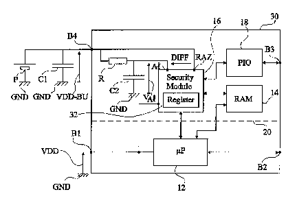
Fig. 2 shows an embodiment of a cryptoprocessor 30
according to the present invention which enables to prevent the
access to critical data during variations of backup supply
voltage VDD_BU. The elements common with cryptoprocessor 10 of
Fig. 1 are designated with the same reference numerals. Crypto-
processor 30 comprises all the elements of cryptoprocessor 10
and further comprises an additional capacitor C2 having a
terminal connected to a source of a reference voltage, for exam-
ple, ground GND of the reader, and having its other terminal
connected on the one hand to a terminal Al of security module 16
and on the other hand to terminal B4 via a device R (for exam-
ple, a resistor, a diode or other) forbidding a fast discharge
of capacitor C2 by an external action on terminal B4. Terminal
B4 is further directly connected to a terminal PAZ of security
module 16. Call DIFF the voltage between terminals Al and PAZ,
and VAl the voltage across capacitor C2. Security module 16 com-
prises an additional RAM 32 (Register) of decreased capacity
with respect to RAM 14 and for which the read and write opera-
tions may be carried out by processing unit 16 over a small
number of clock cycles and at a low power cost. It for example
is a register of a few hundreds of bits, for example, 256 bits.
In the present embodiment, the critical data are
stored in memory 14 in encrypted form, the used encrypted method
CA 02687582 2009-11-17
implementing at least one key, called primary key. The primary
key is stored in additional memory 32 of security module 16. In
normal operation, when microprocessor 12 desires to use critical
data stored in memory 14, it also reads the primary key stored
5 in additional memory 32 to decrypt the critical data stored in
memory 14. On detection of an unauthorized access attempt,
security module 16 first deletes the primary key stored in addi-
tional memory 32 then may delete the critical data stored in
memory 14.
10 In
case of an interruption of main supply VDD, micro-
processor 12 stops operating and security module 16 keeps on
operating by being powered by cell P. Capacitor C2 is charged by
backup Supply voltage VDD_BU applied to terminal B4. Voltage Vpil
is also equal to backup supply voltage VDD_BU. Voltage DIFF is
then substantially zero. In the case where backup supply voltage
VDD BU varies, which for example corresponds to a deactivation
of cell P or to an intentional manipulation of voltage VDD_BU,
the voltage at terminal RAZ varies while voltage VA1 at terminal
Al is maintained at a substantially constant value by capacitor
C2. The increase in absolute value of voltage DIFF is detected
by security module 16 as an unauthorized access attempt, for
example when it is greater than a determined threshold for a
given number of clock cycles. Since backup supply voltage VDD_BU
may have decreased, security module 16 is then powered by addi-
tional capacitor C2 until it is discharged. An unauthorized
access attempt having been detected, security module 16 first
deletes the primary key stored in secondary memory 32. Then, if
its power supply is sufficient, security module 16 attempts to
delete the critical data stored in memory 14.
The size of additional memory 32 being small, the
operation of deleting the data stored in additional memory 32
may be carried out rapidly with a low energy cost. In particu-
lar, it may be performed while security module 16 is only being
powered by capacitor C2. However, according to the size of RAM
14, the capacitance of capacitor C2 may be insufficient to
CA 02687582 2009-11-17
11
ensure a sufficient power supply of security module 16 enabling
to delete all the critical data stored in memory 14. But even if
the power supply of security module 16 by capacitor C2 is insuf-
ficient to enable the deleting of all the critical data stored
in memory 14 and even if backup supply voltage VDD_BU is taken
to a value for which the operation of security module 16 is
disturbed so that it is then no longer able to delete the
remaining critical data stored in memory 14, the remaining crit-
ical data stored in memory 14 are no longer usable since the
primary key stored in additional memory 32 has been deleted. The
critical data remaining in memory 14 are then no longer accessi-
ble.
As an example, the capacitance of capacitor C2 may be
smaller than a few picofarads. Such a capacitance is sufficient
to ensure a power supply current of security module 16 on the
order of a few hundreds of nanoamperes for a few clock cycles.
This is sufficient to ensure the operation of security module 16
for the few clock cycles necessary to detect an intrusion
attempt and to delete additional memory 32. In particular, when
additional memory 32 corresponds to a register, the deleting of
the data stored in memory 32 may be performed in a single clock
cycle. Capacitor C2 may be integrated with the other elements of
security module 16. As an example, capacitor C2 may correspond
to the stray capacitances of MOS transistors forming security
module 16. Further, since capacitor C2 powers security module
16, the constraints of protection of cell P. of capacitor Cl,
and of the electric connection between cell P, capacitor Cl, and
access terminal B4 may be less strict than for the circuit shown
in Fig. 1.
Specific embodiments of the present invention have
been described. Various alterations and modifications will occur
to those skilled in the art. In particular, although the present
invention has been described in the case of a cryptoprocessor
connected to a main power supply source and to a backup supply
source, it should be clear that it may apply to a cryptopro-
CA 02687582 2009-11-17
12
cessor connected to a single supply source, the additional capa-
citor integrated to the cryptoprocessor being then charged by
the single power supply source, and the voltage provided by the
single power supply source being compared with the voltage
across the additional capacitor by the security module for the
detection of an unauthorized access attempt.