Note: Descriptions are shown in the official language in which they were submitted.
CA 02688576 2009-11-27
WO 2008/144906 PCT/CA2008/001004
1
APPLICATIONS FOR SCANNING TUNNELLING MICROSCOPY
CROSS-REFERENCE TO RELATED APPLICATIONS
[0001] This application claims the benefit of priority from United States
provisional
application serial no. 60/932,381 filed May 31, 2007.
FIELD OF THE INVENTION
[0002] This invention relates to scanning tunneling microscopy in general, and
the use of
scanning tunneling microscopy to transfer particles from one location to
another in
particular.
BACKGROUND OF THE INVENTION
[0003] Nanofabrication is the design and manufacture of devices with
dimensions
measured in nanometers, or units measuring 10-9 meters. Nanofabrication has
potential
applications in many fields such as computer and/or electronic technologies,
aerospace
technologies, and medical and/or biotechnologies. For example, nanofabrication
techniques have the potential to offer super-high-density microprocessors and
memory
chips that could advance computer and computer-related technologies.
[0004] There are several ways that nanofabrication might be done. One
traditional
method involves nanolithography. Nanolithography is the process of etching,
writing, or
printing at the microscopic level, where the dimensions of characters are on
the order of
nanometers. For example, individual atoms may be manipulated using the tip of
a
scanning tunneling microscope (STM). However, the utility of STM in
nanofabrication
techniques is traditionally limited to the manipulation of atoms and small
inorganic
molecules such as Xe, CO, metal atom clusters, or metal nanoparticles commonly
having
diameters greater than 10 nanometers, such as gold nano-particles or silver
nanoparticles.
[0005] Nanoscale substances can also be transferred from one point to another
using a
scanning probe microscope (SPM). Korean Application No. 10-2004-0094982
discloses
the use of a scanning probe microscope to transfer a substance from the SPM
tip to a
surface. The SPM tip is submerged in a solution having a voltage potential,
which results
in the SPM having a bias voltage that is opposite the polarity of the target
substance in the
solution. The bias voltage enables the substance to be collected onto the tip.
The
SUBSTITUTE SHEET (RULE 26)
CA 02688576 2009-11-27
WO 2008/144906 PCT/CA2008/001004
2
substance is then transferred to a desired surface in a wet state and before
the tip contacts
the surface the tip bias is removed. By this method, substances are deposited
imprecisely
and necessarily densely since deposition occurs due to capillary action upon
the SPM tip
contacting the surface. Therefore, the number of particles and the precise
location of
deposition cannot be controlled using this method.
SUMMARY OF THE INVENTION
[0006] In one aspect, the present invention provides methods of selectively
transferring
nano-sized material from one location to another using STM where the number of
particle
material and the location of deposition can be precisely controlled by varying
the polarity
of the potential, pulse period, and the clearance between the STM tip and a
surface. These
methods include providing a stylus having a bias, providing the material,
providing a
surface, and changing the bias of the stylus such that the material transfers
from one
location to another.
[0007] One aspect of the present invention provides methods of using a STM to
selectively transfer at least one particle from one location to another by
providing a stylus
having a bias, providing a surface, providing at least one particle, and
changing the bias of
the stylus such that at least one particle transfers from one location to
another.
[0008] Another aspect of the present invention provides methods of using a STM
to
selectively transfer at least one protein molecule from one location to
another by providing
a stylus having a bias, providing a surface, providing at least one protein
molecule, and
changing the bias of the stylus bias such that at least one protein molecule
transfers from
one location to another.
[0009] Another aspect of the present invention provides methods of creating a
design on a
surface by transferring at least one protein from a stylus to the surface.
This transfer is
accomplished by providing a stylus having a bias, providing at least one
protein, providing
a surface, and changing the bias of the stylus bias such that a single protein
transfers from
the stylus to the surface.
[0010] Another aspect of the present invention provides the removal of at
least one
protein from a surface using a STM, by providing a stylus having a bias,
providing a
surface, providing at least one protein on the surface, wherein the bias has a
magnitude
and polarity sufficient to transfer at least one protein from the surface to
the stylus when
the stylus is raster scanned over the surface.
SUBSTITUTE SHEET (RULE 26)
CA 02688576 2009-11-27
WO 2008/144906 PCT/CA2008/001004
3
[0011] Another aspect of the present invention provides the removal of a
single protein
from a surface using STM, by providing a stylus having a bias, providing a
surface,
providing a protein on the surface, and changing the bias of the stylus such
that the protein
is transferred from the surface to the stylus.
BRIEF DESCRIPTION OF THE DRAWINGS
[0012] FIG. I is an STM-generated image of an annealed gold surface without
any
particles;
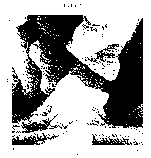
[0013] FIG. 2 is an STM-generated image of an annealed gold surface on which
single (3-
LG molecules are deposited in accordance to one embodiment of the present
invention;
[0014] FIG. 3 is an STM-generated image of a gold surface printed with the
design
"CACN" in accordance to one embodiment of the present invention;
[0015] FIG. 4 is an STM-generated image of a gold surface printed with the
design
"ACMA" in accordance to one embodiment of the present invention; and
[00161 FIG. 5 is an STM-generated image of a gold surface having a partially
erased
"ACMA" design in accordance to one embodiment of the present invention;
[0017] FIG. 6A is an STM-generated image of a gold surface having three nano-
patterns
of (3-LG molecules deposited in accordance to one embodiment of the present
invention;
[0018] FIG. 6B is an STM-generated image of a gold surface having a series of
nano-
patterns of (3-LG molecules deposited in decreasing potential in accordance to
one
embodiment of the present invention;
[0019] FIG. 7 is an STM-generated image of a gold surface having nano-patterns
deposited in overlap and deposited separately in accordance to one embodiment
of the
present invention;
[0020] FIG. 8A is an STM-generated image of a gold surface having a long nano-
band
deposited in accordance to one embodiment of the present invention;
[0021] FIG. 8B is an STM-generated image of a gold surface having a wide nano-
band
depositing in accordance to one embodiment of the present invention;
[0022] FIG. 9A is an STM-generated image of a gold surface having four nano-
patterns of
multiple (3-LG molecules deposited in accordance to one embodiment of the
present
invention; and
SUBSTITUTE SHEET (RULE 26)
CA 02688576 2009-11-27
WO 2008/144906 PCT/CA2008/001004
4
[0023] FIG. 9B is an STM-generated image of a gold surface having a series of
nano-
patterns of multiple (3-LG molecules deposited in accordance to one embodiment
of the
present invention.
DETAILED DESCRIPTION OF THE INVENTION
1. DEFINITIONS
[0024] As used herein, a"protein" or "protein molecule" is an organic compound
made of
amino acids arranged in a linear chain and joined together by peptide bonds
between the
carboxyl and amino groups of adjacent amino acids. Examples of proteins
include (3-
lactoglobulin ([3-LG), bovine serum albumin (BSA), lysozyme, or immunoglobin G
(IgG).
[0025] As used herein, a "stylus" or "tip" is an atomically sharp probe for
use in scanning
tunneling microscopy, which when electrically charged and brought sufficiently
close to a
surface, can deliver a tunneling current between the conducting or
semiconducting surface
atoms and the tip.
[0026] As used herein, "biomolecule" refers to protein, DNA, RNA, or other
biological
compounds and mixtures thereof. Protein is defined above.
[00271 As used herein, a "surface" is the outer or the topmost boundary of an
object or a
material layer constituting such a boundary. A surface can comprise any plane
or contour.
Surfaces suitable for the present invention are those surfaces that are
capable of being
scanned using STM. For example, these surfaces are semiconducting or
conducting.
[0028] A "bias" or "voltage bias" is a steady state voltage. A "change in
bias" or
"changing the bias" refers to a change or the act of changing the magnitude
and/or polarity
of a bias. The change lasts for a duration sufficient to transfer at least one
particle from
one location to another (e.g., the duration can be extended, i.e., lasting I
second or longer,
or temporary, i.e., lasting for less than I second). For example, a bias may
undergo a
change in magnitude and polarity that lasts for a fraction of a second (e.g.,
from about
0.001 milliseconds to about 10 milliseconds, from about 0.75 milliseconds to
about 1.25
milliseconds, or from about 0.9 milliseconds to about 1.1 milliseconds.) In
another
example, a bias is changed from about +0.5V to about -0.5V for a period of
about I
millisecond (e.g., from about 0.5 milliseconds to about 1.5 milliseconds).
Another
example of a change in bias includes changes in bias within the range +5.0 V
to about -
5.0 V.
SUBSTITUTE SHEET (RULE 26)
CA 02688576 2009-11-27
WO 2008/144906 PCT/CA2008/001004
[0029] As used herein, "conductive material" is any material that conducts
electric current
when an electrical potential difference is applied across two different points
on the
material. Exemplary conductive materials include conductors and semi-
conductors. Other
exemplary conductive material includes metals (e.g., copper, iron, gold,
silver, platinum,
palladium, ruthenium, rhodium, osmium, iridium, zinc, nickel, aluminum,
silver, titanium,
mercury, chromium, cadmium, alloys thereof, and the like), graphite, solutions
of salts,
plasmas, some glasses (e.g., silicon), or conducting or semiconducting
polymers.
[0030] As used herein, "STM" refers to a scanning tunneling microscope or
scanning
tunneling microscopy.
[0031] As used herein, "material" refers to at least one particle, at least
one biomolecule,
and/or at least one protein molecule. For example, 'material' refers to a
single particle or a
plurality of particles. In another example, material refers to a single
protein molecule or a
plurality of protein molecules, where the protein molecules may be of the same
kind (e.g.,
chemically identical protein molecules) or of a different kind (e.g.,
chemically different
protein molecules).
[0032] As used herein, "transferring" or "transfer" means conveying material
(e.g., at least
one particle (e.g., at least one atom, at least one ion, at least one molecule
(e.g.,
biomolecule), or the like)) from one place to another. For example,
'transferring' can
describe conveying at least one particle (e.g., at least one protein molecule)
from a stylus
to a surface or conveying at least one particle (e.g., at least one protein
molecule) from a
surface to a stylus.
[0033] As used herein, "selectively transferring" refers to the transfer of a
particle from a
desired location to another desired location. Transferring is defined above.
[0034] As used herein, "particle" refers to an atom, an atom cluster, i.e., a
non-covalently
bonded group of atoms), or a molecule (e.g., a biomolecule, (e.g., a protein
molecule,
DNA, or RNA)).
II. STM TECHNOLOGY
[0035] In the present invention, it has been discovered that Scanning
Tunneling
Microscopy is a useful tool for fabrication on a nano-sized scale by
selectively transferring
material (e.g., at least one particle (e.g., at least one protein)) from one
location to another
location.
SUBSTITUTE SHEET (RULE 26)
CA 02688576 2009-11-27
WO 2008/144906 PCT/CA2008/001004
6
[0036] STM employs a stylus that has been treated so that it has an atomically
sharp tip.
When a potential difference is applied to a stylus and the stylus is brought
sufficiently
close to a surface, a tunneling current flows between the surface and the
stylus. The
tunneling current (1) is measured from the variation in the bias voltage, or
bias, (U)
between the stylus and the surface at the measurement point. The tunneling
current I can
be expressed as:
I= K X U X e-(kxd) (I)
[0037] where K and k are constants, U is the tunneling bias, and d is the
distance between
the stylus and the surface. Based on the relationship expressed in equation
(1), the
tunneling current is directly dependent on the bias, U, and the distance
between the stylus
and the surface, d. Furthermore, the tunneling current undergoes exponential
decay as the
distance between the stylus and the surface increases. At a separation of a
few atomic
diameters, the tunneling current rapidly increases as the distance between the
stylus and
the surface decreases when the stylus maintains a constant bias. This rapid
change of
tunneling current with distance results in atomic resolution when the tip is
raster scanned
over the surface to produce an image.
[0038] However, the present invention employs STM to selectively transfer
material from
one location to another location. This method is useful for creating a
nanometer-scaled
design on a surface by selectively depositing material (e.g., protein
molecules) or by
selectively removing material (e.g., protein molecules) from a surface.
III. TRANSFERRING PARTICLES USING STM
[0039] The methods of the present invention are useful for selectively
transferring
material from a first location to a second location comprising providing a
stylus having a
bias, providing a surface, providing material, and changing the bias of the
stylus such that
material is transferred from the first location to the second location,
wherein the material
comprises at least one particle (e.g., at least one protein molecule).
[0040] As shown in FIG. 1, an annealed gold surface without any particles
deposited onto
it appears as smooth terraces. The (3-lactoglobulin ((3-LG) particles were
removed or
erased from the surface by scanning the surface with the (3-LG-coated stylus
with the
stylus bias set to +0.5 V (surface as reference).
[0041] Reversing the stylus bias to -0.5 V (surface as reference) causes
particles such as
[3-LG to be deposited onto the annealed gold surface. As shown in FIG. 2,
scanning the
SUBSTITUTE SHEET (RULE 26)
CA 02688576 2009-11-27
WO 2008/144906 PCT/CA2008/001004
7
surface with the (3-LG-coated stylus biased to -0.5 V (surface as reference)
results in single
(3-LG molecules being deposited evenly onto the gold surface from the stylus
when the
stylus is raster scanned over the gold surface.
[0042] It is also a feature of the present invention that the amount of
material transferred
(e.g., at least one particle (e.g., at least one protein molecule)) and the
precision of material
deposition is tunable approximately in accordance with the relationship
expressed in
equation (1) above. Thus, the amount of material transferred and the precision
with which
it is transferred can be adjusted by changing the bias and/or changing the
distance between
the stylus and the surface. For example, when the distance between the surface
and the
stylus, i.e., clearance, is increased by about 0.1 nm, and the bias undergoes
a given change,
a plurality of particles can be deposited onto a surface. However, when the
distance
between the surface and the stylus is increased by about 0.5 nm, and the bias
undergoes
the same change, a single particle can be deposited onto the surface.
[0043] Surfaces can also be printed with a desired design (FIGS. 3-5).
Furthermore, the
number of molecules deposited and the location of deposition can be selected
by
controlling the bias potential and the pulse duration. In FIG. 3, a gold
surface was printed
with the design "CACN" using bias pulses of -3.0 V and 1 millisecond pulse
duration,
where each nanopattern consists of about a dozen [3-LG molecules. Each letter
in the
string "CACN" fabricated or written with small nanopatterns are only 70 nm in
height.
Each pattern consisting of several single molecules was smaller than 20 nm.
[0044] In FIG. 4, a gold surface was printed with the design "ACMA" using bias
pulses of
-3.2 V and 1 millisecond pulse duration, where each nanopattern consists of
one or a
couple of P-LG molecules, forming characters no more than 40 nm in height.
Subsequently scanning a desired location on the gold surface using a reversed
bias
potential will erase the design. Shown in FIG. 5 is another printed gold
surface with an
"ACMA" design where subsequently the upper portion of the design has been
erased.
[0045] One aspect of the present invention provides a method of selectively
transferring at
least one particle from a first location to a second location comprising
providing a stylus
having a bias, providing a surface, providing at least one particle, and
changing the bias of
the stylus such that at least one particle transfers from the first location
to the second
location.
[0046] Another example provides a method of selectively transferring at least
one protein
molecule from a first location to a second location comprising providing a
stylus having a
SUBSTITUTE SHEET (RULE 26)
CA 02688576 2009-11-27
WO 2008/144906 PCT/CA2008/001004
8
bias, providing a surface, providing at least one protein molecule, and
changing the bias of
the stylus such that at least one protein molecule transfers from the first
location to the
second location.
[0047] In several examples, STM is used to selectively deposit at least one
particle (e.g.,
at least one protein molecule) on a surface or selectively remove at least one
particle (e.g.,
at least one protein) from a surface by changing the bias of the stylus, such
that at least one
particle (e.g., at least one protein molecule) is transferred from the stylus
to a selected
location on the surface or at least one particle (e.g., at least one protein
molecule) is
transferred from a selected location on the surface to the stylus. In one
example, at least
one particle (e.g., at least one protein molecule (e.g., P-LG, BSA, lysozyme,
IgG, or the
like)) is transferred from a stylus to a selected location on a surface by
changing the
polarity and/or magnitude of the bias of the stylus. In another example, at
least one
particle (e.g., protein molecule (e.g., P-LG, BSA, lysozyme, IgG, or the
like)) is
transferred from a selected location on a surface to a stylus by changing the
polarity and/or
magnitude of the bias of the stylus. In another example, at least one particle
(e.g., protein
molecule (e.g., P-LG, BSA, lysozyme, IgG, or the like)) is transferred from a
stylus to a
selected location on a surface by changing the polarity and/or magnitude of
the bias of the
stylus, and changing the distance between the stylus and the surface. In
another example,
at least one particle (e.g., protein molecule (e.g., P-LG, BSA, lysozyme, IgG,
or the like))
is transferred from a selected location on a surface to a stylus by changing
the polarity
and/or magnitude of the bias of the stylus, and changing the distance between
the stylus
and the surface.
[0048] Another aspect of the present invention provides a method of
selectively
transferring a single particle (e.g., protein molecule) from a first location
to a second
location by providing a stylus having a bias, providing a surface, providing a
single
particle (e.g., protein molecule), and changing the bias of the stylus. For
example, a single
particle (e.g., protein molecule (e.g., P-LG, BSA, lysozyme, IgG, or the
like)) is
transferred from a stylus to a selected location on a surface by changing the
bias of the
stylus such that a single particle (e.g., protein molecule (e.g., P-LG, BSA,
lysozyme, IgG,
or the like)) is transferred. For instance, a single particle (e.g., protein
molecule (e.g., 0-
LG, BSA, lysozyme, IgG, or the like)) is transferred from a stylus to a
selected location on
a surface by changing the polarity and/or the magnitude of the bias of the
stylus such that a
single particle (e.g., protein molecule (e.g., P-LG, BSA, lysozyme, IgG, or
the like)) is
SUBSTITUTE SHEET (RULE 26)
CA 02688576 2009-11-27
WO 2008/144906 PCT/CA2008/001004
9
transferred. In another example, a single particle (e.g., protein molecule
(e.g., P-LG, BSA,
lysozyme, IgG, or the like)) is transferred from a stylus to a selected
location on a surface
by changing the polarity and/or the magnitude of the bias of the stylus and
changing the
distance between the stylus and surface such that a single particle (e.g.,
protein molecule
(e.g., P-LG, BSA, lysozyme, IgG, or the like)) is transferred.
[0049] In one example, at least one protein molecule (e.g., P-LG, BSA,
lysozyme, IgG, or
the like) is transferred from a stylus to a selected location on a surface by
changing the
bias from about +5.0 V to about -5.0 V for a duration sufficient to transfer
the protein
molecule(s). In another example, at least one protein molecule (e.g., P-LG,
BSA,
lysozyme, IgG, or the like) is transferred from a stylus to a selected
location on a surface
by changing the bias from about +0.5 V (e.g., from about +1.0 V to about +0.1
V) to about
-4.5 V (e.g., from about -0.1 V to about -3.6 V, or from about -0.5 V to about
-3.2 V) for a
duration of about 1 millisecond (e.g., from about 0.001 milliseconds to about
10
milliseconds, from about 0.5 milliseconds to about 1.5 milliseconds, or from
about 0.7
milliseconds to about 1.3 milliseconds). In one example, at least one protein
molecule
(e.g., P-LG, BSA, lysozyme, IgG, or the like)) is transferred from a stylus to
a selected
location on a surface by changing the bias from about +0.5 V (e.g., from about
+1.0 V to
about +0.1 V) to about -4.5 V (e.g., from about -0.1 V to about -3.6 V, or
from about -0.5
V to about -3.2 V) for a duration of about 1 millisecond (e.g., from about 0.5
milliseconds
to about 1.5 milliseconds, or from about 0.7 milliseconds to about 1.3
milliseconds) and
increasing the distance between the stylus and the surface by about 0.2 nm
(e.g., from
about 0.05 nm to about 0.21 nm, or from about 0.05 nm to about 0.20 nm).
[0050] Another aspect of the present invention provides a method of removing
at least one
protein molecule (e.g., P-LG, BSA, lysozyme, IgG, or the like)) from a desired
location on
a surface comprising providing a stylus having a bias, providing a surface,
providing at
least one protein on the surface, and changing the bias such that at least one
protein
molecule is transferred from the surface to the stylus. In one example, at
least one protein
molecule (e.g., P-LG, BSA, lysozyme, IgG, or the like)) is transferred from a
selected
location on a surface to a stylus to a selected location on a surface by
changing the bias
from about -4.5 V (e.g., from about -3.6 V to about -0.1 V, or from about -3.2
V to about -
0.5 V, or about -0.5 V)) to about +0.5 V (e.g., from about +1.0 V to about
+0.1 V) for a
duration sufficient to transfer the protein(s).
SUBSTITUTE SHEET (RULE 26)
CA 02688576 2009-11-27
WO 2008/144906 PCT/CA2008/001004
[0051] Another aspect of the present invention provides a method of
selectively
transferring at least one protein comprising providing a stylus having a bias,
providing a
surface, providing at least one protein, and changing the bias such that a
single protein is
transferred, wherein the protein has a mass of about 5 kDa. In several
examples, the
protein has a mass of at least 10 kDa (e.g., at least 15 kDa, at least 20 kDa,
at least 50 kDa,
or at least 100 kDa). In other examples, the protein has a mass of from about
5 kDa to
about 200,000 kDa (e.g., from about 10 kDa to about 180,000 kDa, or from about
20 kDa
to about 150,000 kDa). For instance, at least one protein molecule having a
mass of at
least 5 kDa is transferred from a stylus to a selected location on a surface
by changing the
bias from about +0.5 V (e.g., from about +1.0 V to about +0.1 V) to about -4.5
V (e.g.,
from about -0.1 V to about -3.6 V, or from about -0.5 V to about -3.2 V) for a
duration of
about 1 millisecond (e.g., from about 0.5 milliseconds to about 1.5
milliseconds, or from
about 0.7 milliseconds to about 1.3 milliseconds). In another instance, at
least one protein
molecule having a mass of at least 15 kDa is transferred from a stylus to a
selected
location on a surface by changing the bias from about +0.5 V (e.g., from about
+1.0 V to
about +0.1 V) to about -4.5 V (e.g., from about -0.1 V to about -3.6 V, or
from about -0.5
V to about -3.2 V) for a duration of about 1 millisecond (e.g., from about 0.5
milliseconds
to about 1.5 milliseconds, or from about 0.7 milliseconds to about 1.3
milliseconds) and
increasing the distance between the stylus and the surface by about 0.2 nm
(e.g., from
about 0.05 nm to about 0.21 nm, or from about 0.05 nm to about 0.20 nm).
[0052] An alternative aspect of this invention provides a method of
selectively transferring
a protein from one location to another location comprising providing a stylus
having a
bias, providing a surface, providing a protein, and changing the bias such
that a single
protein is transferred, wherein the protein comprises at least 50 amino acids
(e.g., at least
60 amino acids, at least 75 amino acids, at least 100 amino acids, at least
150 amino acids,
or at least 300 amino acids) wherein each residue is independently selected
from alanine,
cysteine, aspartic acid, glutamic acid, phenylalanine, glycine, histidine,
isoleucine, lysine,
leucine, methionine, asparagines, proline, glutamine, arginine, serine,
threonine,
selenocysteine, valine, tryptophan, and tyrosine, including variations on
these amino acids
and other similar molecules incorporated into proteins. In several examples,
the protein
comprises from about 100 amino acids to about 600 amino acids, each of which
is
independently selected from the abovementioned list of amino acids.
SUBSTITUTE SHEET (RULE 26)
CA 02688576 2009-11-27
WO 2008/144906 PCT/CA2008/001004
11
[0053] It is recognized that molecules transferable using the present methods
are not
restricted to these proteins or even biomolecules.
[0054] Another aspect of the present invention provides a method of
selectively
transferring at least one P-LG molecule or at least one BSA molecule from a
first location
to a second location comprising providing a stylus having a bias, providing a
surface,
providing at least one P-LG molecule or at least one BSA molecule, and
changing the bias
such that at least one P-LG molecule or at least one BSA molecule is
transferred from the
first location to the second location. For example, STM is used to selectively
deposit a
single P-LG molecule or a single BSA molecule on a surface or selectively
remove a
single P-LG molecule or a single BSA molecule from a surface by changing the
bias of the
stylus such that the P-LG molecule or BSA molecule is transferred from the
stylus to a
selected location on the surface or from a selected location on the surface to
the stylus. In
one example, a single P-LG molecule or a single BSA molecule is transferred
from a
stylus to a selected location on a surface by changing the polarity and/or
magnitude of the
bias of the stylus for a duration sufficient to transfer the P-LG molecule or
the BSA
molecule. In another example, a single P-LG molecule or a single BSA molecule
is
transferred from a selected location on a surface to a stylus by changing the
polarity and/or
magnitude of the bias of the stylus for a duration sufficient to transfer the
(3 -LG molecule
or the BSA molecule. In other examples, at least one P-LG molecule or at least
one BSA
molecule is transferred from a selected location on a surface to a stylus by
changing the
polarity and/or magnitude of the bias of the stylus, and changing the distance
between the
stylus and the surface. In still other examples, a single P-LG molecule or a
single BSA
molecule is transferred from a stylus to a selected location on a surface by
changing the
polarity and/or magnitude of the bias of the stylus, and changing the distance
between the
stylus and the surface.
[0055] Another aspect of the present invention provides a method of
selectively
transferring at least one protein molecule comprising providing a stylus
having a bias,
providing a surface, providing at least one protein molecule, and changing the
polarity
and/or magnitude of the bias such that the protein molecule(s) is transferred,
wherein the
protein molecule(s) has a positive net charge when subjected to a neutral
buffered
environment. Another aspect of the present invention provides a method of
selectively
transferring a protein comprising providing a stylus having a bias, providing
a surface,
providing a protein, and changing the polarity and/or magnitude of the bias
such that a
SUBSTITUTE SHEET (RULE 26)
CA 02688576 2009-11-27
WO 2008/144906 PCT/CA2008/001004
12
single protein is transferred, wherein the protein has a negative net charge
when subjected
to a neutral buffered environment. Exemplary proteins include (3-LG, BSA,
lysozyme, or
IgG.
[0056] Another aspect of the present invention provides a method of
selectively
transferring a protein comprising providing a stylus having a bias, providing
a surface,
providing a protein, and changing the bias of the stylus such that a single
protein is
transferred, wherein the stylus comprises a conductive material. For example,
the stylus
comprises at least one metal, e.g., gold, silver, platinum, palladium,
ruthenium, rhodium,
osmium, iridium, tungsten, or combinations thereof. In other examples, the
stylus
comprises platinum and iridium. In other examples, the stylus comprises
essentially
platinum and iridium in any proportion. For instance, the stylus further
comprises about
80 wt % (e.g., from about 70 wt % to about 90 wt %) of platinum and about 20
wt % (e.g.,
from about 30 wt % to about 10 wt %) of iridium.
[0057] Another aspect of the present invention provides methods of selectively
transferring a protein from a stylus to a gold surface or from a gold surface
to a stylus by
providing a gold surface, providing a protein, providing a stylus having a
bias, and
changing the bias of the stylus such that a protein transfers from a stylus to
a gold surface
or from a gold surface to a stylus. Surfaces suitable for the present
invention include any
contour. However, surfaces suitable for use in the present invention include
any surface
that is suitable for STM scanning. Such surfaces include those that are
conducting or
semiconducting. Examples of several surfaces include those comprising a
conductor or a
semiconductor. In other examples, a surface comprises gold, silver, platinum,
copper,
palladium, ruthenium, rhodium, osmium, tungsten, iridium, zinc, nickel,
aluminum, iron,
titanium, chromium, graphite, mercury, silicon, silicon dioxide, combinations
thereof, or
the like.
[00581 The change in bias can refer to a change in magnitude and/or polarity
of a bias for
a duration of time sufficient to transfer at least one particle (e.g., at
least one protein
molecule (e.g., at least one [3-LG, BSA, lysozyme, IgG, or the like)). The
change can be
extended, i.e., more than 1 second, or the change can be temporary, i.e., 1
second or less.
For example, a bias undergoes a change in magnitude and/or polarity that lasts
for a
fraction of a second (e.g., from about 0.25 milliseconds to about 2.5
milliseconds, from
about 0.75 milliseconds to about 1.25 milliseconds, or from about 0.9
milliseconds to
about 1.1 milliseconds) that constitutes a pulse. When the transfer of at
least one particle
SUBSTITUTE SHEET (RULE 26)
CA 02688576 2009-11-27
WO 2008/144906 PCT/CA2008/001004
13
(e.g., at least one protein molecule (e.g., at least one (3-LG, BSA, lysozyme,
IgG, or the
like)) conveys the particle(s) from a stylus to a selected location on a
surface, the change
in bias lasts for a sufficient time to convey the particle(s) to the selected
location on the
surface (e.g., the bias change is temporary). When the transfer of at least
one particle
(e.g., protein molecule (e.g., (3-LG, BSA, lysozyme, IgG, or the like))
conveys the
particle(s) from a selected location on a surface to a stylus, the change in
bias also lasts for
a sufficient time to convey the particle(s) to the selected location on the
surface (e.g., the
bias change is temporary or extended). For example, when transferring several
particles
from a desired location or area of a surface to a stylus, the change in bias
lasts at least for a
time sufficient to raster the stylus over desired location or area of the
surface or position
the stylus over the particle(s).
[0059] In other examples, the magnitude of the bias is changed for a brief
amount of time
or an extended amount of time. For instance, the bias is changed from about
+0.1 V to
about -0.5 V for about 1 millisecond. In another instance, the bias is changed
from about
+0.1 V to about -0.8 V for about 1 millisecond.
[0060] As noted above, the amount of material that is transferred from one
location to
another location and the change in bias necessary to accomplish the transfer
depends on
the clearance, i.e., the distance between the stylus and the surface. For
example, the
clearance can be tuned to transfer a desired amount of material from one
location to
another (e.g., from a stylus to a surface or from a surface to a stylus). As
such, the
clearance can be tuned to facilitate the transfer. For example, the clearance
can be
increased or decreased to provide the transfer of a desired amount of material
from a first
location to a second location. Furthermore, the clearance can be increased or
decreased to
improve or exacerbate the precision of material deposition from a stylus onto
a surface.
For example, the clearance can be increased or decreased by as much as about
0.3 nm
(e.g., up to about 0.25 nm, or up to about 0.20 nm) to improve or exacerbate
the precision
of material deposition from a stylus onto a surface.
[0061] Another aspect of the present invention provides a method of producing
a biochip
comprising using STM to selectively transfer at least one protein molecule
from a first
location (e.g., a stylus) to a second location (e.g., surface) comprising
providing a stylus
having a bias, providing a surface, providing at least one protein molecule,
and changing
the bias of the stylus such that at least one protein molecule is transferred.
SUBSTITUTE SHEET (RULE 26)
CA 02688576 2009-11-27
WO 2008/144906 PCT/CA2008/001004
14
[0062] According the methods of the present invention, designs can be created
"top down"
or "bottom up" wherein at least one particle is added to a surface to create a
design, or at
least one particle is removed from a surface to create a design.
IV. EXAMPLES
[0063] Proteins were dissolved at a concentration of 1.0 g/mL in 100 mM
phosphate
buffer (pH 7.0). Gold coated cover slips were employed as substrates, which
were
annealed at about 820 C for two hours in order to attain atomically flat
terraces as shown
in FIGS. 1 and 2. A stylus made of Pt and Ir (Pt:lr, 80:20 wt%) was cut
manually and
calibrated to make sure it was atomically sharp at its end. The stylus was
then coated with
biomolecules. The stylus was soaked in the buffer containing the proteins. No
bias
potential is needed to coat the stylus with the target biomolecules. The
stylus was then
removed and allowed to air dry. The STM tunneling current was set at about 0.1
nA.
Transferring of the protein was accomplished using two modes as follows:
[0064] 1. Scanning mode: In this mode, the protein coated tip was employed.
The
deposition was accomplished by scanning over an area, and removal or erasure
of the
proteins was accomplished by scanning over the same area with a changed bias.
In the
whole process, the tip was engaged in tunneling state and when the bias was
changed, it
was changed to a certain value that was maintained until the next change.
[0065] Using the protein coated Pt-Ir tip, the clean annealed gold sample
illustrated in
FIG. I was scanned using STM in a normal stable imaging mode at a bias set at
+0.5 V.
When the (3-LG coated tip bias was set to -0.5 V, (3-LG molecules were
transferred evenly
onto the gold surface when the tip was in scanning mode as illustrated in FIG.
2. The
transferring rate is proportional to the bias magnitude and is dependent on
the clearance.
For depositing in scanning mode, the bias ranged from -0.1 V to -2.0 V.
[0066] 2. Pulse mode: This mode was developed in order to deposit molecules
according to a predefined pattern. A protein coated tip was approached to
tunneling state,
and then transfer of the protein was controlled by three factors: pulse bias,
pulse period,
and clearance. Clearance could be changed by the software manually; i.e. raise
the tip by
0.2 nm. In this way, the tip was either raised or lowered in order to control
the density of
the deposited biomolecules on the substrate. By adjusting the additional
clearance and
pulse period and the bias, single molecule manipulation was achieved. In pulse
mode, the
bias change means the bias was changed from an initial value to another value
that was
SUBSTITUTE SHEET (RULE 26)
CA 02688576 2009-11-27
WO 2008/144906 PCT/CA2008/001004
held for a specific length of time and then it was returned to the initial
value; i.e., the
initial bias was -0.5 V, changed to the pulse value of -1.5 V for 1
millisecond, and then
returned to the initial bias of -0.5 V.
[0067] The pulse mode was developed for precision patterning as demonstrated
in FIGS.
3-5. By adjusting the clearance, bias magnitude and bias pulse period, single
molecule
manipulation was achieved. Referring to FIG. 3, a string "ACMA" of single [3-
lactoglobulin molecules was written with the pulse magnitude of -3.2 V. It was
observed
that tip bulk material was transferred when the bias is very high; i.e. for a
Pt-Ir tip and
gold surface, it is normally about 4.0 V. However, no tip bulk material was
observed to
transfer with any smaller bias. With a bias smaller than 4.0 V only protein
molecules are
transferred between the tip and substrate.
[0068] In another example shown in FIG. 6A, three nanopatterns of dozens of (3-
lactoglobulin molecules were deposited onto a gold surface with the release of
three pulses
of -3.0 V and 1 millisecond. In all three nano-fabrications, tips were lifted
up by 0.2 nm
when a pulse was released
[0069] In FIG. 6B, a series of nano-patterns of multiple (3-LG molecules were
deposited
onto a gold surface. Each one corresponds to a bias pulse respectively but of
different
potentials. From left to right, the potential was decreased from -3.1 V to -
3.3 V by a step
of -0.1 V.
[0070] FIG. 7 shows another example where the top pattern consists of two nano-
patterns
deposited and overlapping each other using two pulses at -1.8 V and for 10
milliseconds.
Two nano-patterns deposited separately are shown just below the first pattern.
[0071] FIG. 8A shows another example of a long nano-band generated
corresponding to
the release of a pulse of -1.8 V for 50 milliseconds. FIG. 8B shows a wide
nano-band
generated by depositing three thin ones side by side.
[0072]
[0073] FIG. 9A shows four nano-patterns of multiple (3-LG molecules deposited
onto a
gold surface. The specific shape of the formed nano-patterns is probably due
to the shape
of the tip. Each nano-pattern was formed from a single bias pulse of -2.0 V
for 10
milliseconds, and each pulse resulted in a nano-pattern of a similar shape and
size.
[0074] FIG. 9B shows a series of nano-patterns of multiple (3-LG molecules
deposited
onto a gold surface. Each pattern corresponds to a bias pulse of the same
duration but of
SUBSTITUTE SHEET (RULE 26)
CA 02688576 2009-11-27
WO 2008/144906 PCT/CA2008/001004
16
different potentials. From left to right, the potential was decreased from -
2.6 V to -3.4 V
by an incremental step of -0.2 V.
[0075] The abovementioned examples can also be performed using BSA, which
yields
similar results.
OTHER EMBODIMENTS
[0076] The foregoing discussion discloses and describes merely exemplary
embodiments
of the present invention. One skilled in the art will readily recognize from
such discussion
and from the accompanying drawings and claims, that various changes,
modifications and
variations can be made therein without departing from the spirit and scope of
the invention
as defined in the following claims. For example, a scanning probe microscope
capable of
carrying out the methods of this invention can be used in place of a scanning
tunneling
microscope.
SUBSTITUTE SHEET (RULE 26)