Note: Descriptions are shown in the official language in which they were submitted.
CA 02689613 2009-12-30
DESCRIPTION
Horizontal Junction Field-Effect Transistor
This is a divisional application of Canadian Patent Application Serial
No. 2 395 264 filed on December 6, 2000.
Technical Field
The present invention relates to a transverse junction field effect
transistor (JFET: Junction Field Effect Transistor), and more specifically, it
relates to a transverse junction field effect transistor employed as a power
transistor for electric power.
It should be understood that the expression "the invention" and the
like encompasses the subject-matter of both the parent and the divisional
applications.
Background Technique
A junction field effect transistor (JFET) applies a reverse bias
voltage from a gate electrode to a p-n junction provided on a side portion of
a channel region passing carriers therethrough, thereby spreading a
depletion layer from the p-n junction to the channel region and controlling
the conductance of the channel region for performing operation such as
switching. In a "transverse" JFET, carriers move in parallel with an
element face in the channel region. While the carriers for the channel
may be either electrons (n-type) or holes (p-type), mobility of electrons is
higher as compared with holes in SiC to which the present invention is
directed, and hence the channel region is generally formed by an n-type
impurity region. For the purpose of convenience, therefore, it is assumed
that the carriers for the channel are electrons and hence the channel region
is an n-type impurity region in the following description, while the channel
region may alternatively be formed by a p-type impurity region, as a matter
of course.
SiC, having large mobility of carriers similarly to Si as described
above, a high saturation drift velocity similarly to GaAs and a high
withstand voltage, is subjected to study for application to a high-speed
-1-
CA 02689613 2009-12-30
switching element or a high-power element. Crystal structures of SiC
include a hexagonal closest packing structure and a cubic closest packing
structure, while the hexagonal closes packing structure includes a number of
ones having different cycle periods of layers and at least 100 polytypes
- la -
CA 02689613 2009-12-30
are known. Representative polytypes are 3C, 4H, 6H and the like. C
means cubic and H means hexagonal, while the prefixed numerals express
cycle periods. Only 3C is cubic and referred to as P-SiC, and the
remaining polytypes are referred to as a-SiC as a whole. In the following
description, only 6H or 4H of a-SiC is solely employed.
Fig. 34 is a sectional view showing an exemplary JFET employing
SiC (U.S. Patent No. 5,264,713 granted to John W. Palmour et al.).
Referring to Fig. 34, the conductivity type of an SiC substrate 101 is
preferably the p-type, to define a p-type SiC substrate. The conductivity
type of an SiC film 102 formed on a partial region of the SiC substrate 101
is also preferably the p-type, to define a p-type SiC film 102. Further, an
n-type SiC film 103 is formed on this p-type SiC film 102 to include a
thinned portion 111 corresponding to a channel region. An n+-type
impurity layer 117 coming into ohmic contact with a source electrode 112
and an n+-type impurity layer 118 coming into ohmic contact with a. drain
electrode 113 are formed on the n-type SiC film 103. A gate electrode 114
is formed on the back side of the aforementioned p-type SiC substrate 101
as a back gate 114. Face portions excluding the aforementioned source,
drain and gate electrodes are covered with protective films 126.
In the aforementioned prior art (Fig. 34), the conductivity type of the
SiC substrate is preferably set to the p-type for the following reason: As
hereinabove described, carriers for the channel region are formed by
electrons (n-type), since high mobility is attained. Therefore, the n-type
SiC film defines a layer including the channel region. Thus, the p-type
SiC film defines a layer limiting the carriers in this n-type SiC film in the
periphery. If an n-type SiC substrate is employed as the SiC substrate for
forming this p-type SiC film, a reverse bias voltage is applied to the
junction between the n-type SiC substrate and the p-type SiC film to result
in a depletion layer when a plus potential is applied to the gate electrode.
Therefore, it is necessary to evaluate and determine influence by this
depletion layer. When the p-type SiC substrate is employed to the
contrary, this influence by a depletion layer may not be evaluated and no
reverse bias voltage may be taken into consideration in the junction of the
-2-
CA 02689613 2009-12-30
multilayer part reaching the channel region in on-off action. When the
SiC substrate of the aforementioned conductivity type is employed,
therefore, a high-speed switching element for high power or the like can be
obtained with carriers having high mobility by growing a depletion layer
only in the channel region at need.
However, the p-type SiC substrate has higher defect density of
micropipes or the like as compared with the n-type SiC substrate.
Therefore, the defect density is increased also in a crystal growth layer
essential in fabrication of the semiconductor element such as the JFET.
Reflecting such high defect density, the JFET formed on the p-type SiC
substrate exhibits a low yield for defining a JFET of complete quality, while
a completed JFET exhibits a large leakage current.
In the aforementioned transverse JFET shown in Fig. 34, a forward
bias voltage is applied to the junction between the source region 103 formed
by an n-type impurity region and the p-type impurity layer 102 in an ON-
state. In an OFF-state, a reverse bias voltage is applied to the
aforementioned junction, and a depletion layer grows in the channel region
to block the channel region. In the ON-state, the forward bias voltage is
desirably applied to the junction between the source region 103 formed by
an n-type impurity region and the p-type impurity layer 102, and a current
escapes from the channel region and flows into the gate electrode 114. The
current leaking from the channel region and flowing into the gate electrode
114 increases along with forward bias voltage rise and temperature rise.
'The current leaking from the channel region and flowing into the gate
electrode exerts influence on the amplification factor, and the amplification
factor is problematically lowered when this current increases.
In the transverse JFET shown in Fig. 34, the aforementioned p-n
junction is formed on the overall face of the p-type epitaxial SiC film. As
compared with the area of the part of the channel region in contact with the
bottom of a trench 124, therefore, the area of the aforementioned p-n
junction between the n-type impurity region 103 and the p-type impurity
region is problematically excessive. In other words, the ratio of a part not
contributing to on-off action but defining the path for the aforementioned
-3-
CA 02689613 2009-12-30
current leaking from the channel region is problematically large as
compared with a small ratio of the area of the channel region performing
on-off action in the p-n junction.
Fig. 35 is a schematic sectional view of another conventional
transverse JFET employing SiC (P. A. Ivanov et al.: 4H-SiC Field-Effect
Transistor Hetero-Epitaxially Grown on 6H-SiC Substrate by Sublixnati.on,
p. 757, Silicon Carbide and Related Materials, 1995 Conf., Kyoto, Japan).
Referring to Fig. 35, a 4H-SiC film 109 containing Sn is hetero-epitaxially
grown on a 6H-SiC substrate 101, for defining a buffer layer 109. An SiC
film 102 containing Al serving as a p+-type impurity is formed on the buffer
layer 109, and an n-type SiC film 103 containing nitrogen, having a
channel region 111 arranged on the central portion along with a source
region 117 and a drain region 118 located on both sides thereof is formed
thereon. A source electrode 112 and a drain electrode 113 are provided on
upper portions of the left and right sides of the channel region, and. gate
electrodes 114 are formed on portions downward beyond the source an
drain electrodes through trenches 115. Ni films defining underlayer films
120 and Al films defining upper films 121 are formed as the electrodes 114.
When this transverse JFET is employed, a JFET having high drift mobility
of electrons and extremely high mobility of electrons can be formed.
However, the JFET shown in Fig. 35 has the following problems:
(a) The JFET is insufficient in points of high withstand voltage and
low ON-state resistance.
The withstand voltage of a JFET depends on the withstand voltage
of a p-n junction formed by an n-type impurity region defining a channel
and a p-type impurity region in contact with this region. In order to
improve the withstand voltage of the JFET, therefore, the withstand
voltage of the p-n junction may be improved. While the concentration of
an n-type impurity defining the impurity in the channel may be reduced in
order to improve the withstand voltage of the p-n junction, the quantity of a
current in the channel is reduced and ON-state resistance (resistance in a
state where carriers flow in the channel region) is increased as a result.
Consequently, power is consumed and the element temperature is
-4-
CA 02689613 2009-12-30
increased. A transverse JFET exhibits a negative temperature coefficient
in a large drain current range and hence negative feedback is applied with
respect to temperature rise, while no negative feedback is applied in a
small drain current range. Power consumption in the element is
unpreferable regardless of the value of the drain current. Another reason
for the impossibility of reducing the aforementioned ON-state resistance of
the JFET resides in contact resistance in the electrodes. When each
electrode is made of Ni in the structure shown in Fig. 35, impurity
concentration is so low that Schottky contact tends to remain and ohmic
contact cannot be attained.
(b) The JFET is insufficient in switching speed.
The switching speed depends on the charge/discharge time for a
depletion layer in the p-n junction. Assuming that C represents the
capacitance of the depletion layer and Rg represents gate resistance, the
charge/discharge time is substantially proportionate to the product CRg
thereof. Therefore, the switching time can be quickened if the gate
resistance Rg can be lowered, while the trenches are formed in the second
conductivity region and the gate resistance cannot be sufficiently lowered
in the conventional JFET shown in Fig. 35. When attaching importance to
intuitive grasp while slightly sacrificing correctness, the gate resistance Rg
can be regarded as the resistance of paths reaching the p-n junction
interface on the central portion of the channel 111 from the gate electrodes
114.
(c) Fabrication steps are complicated and require precise and strict
management.
The aforementioned JFET shown in Fig. 35 is fabricated by the
following method: The buffer layer 109 is formed on the SiC substrate 101,
followed by formation of the p+-type SiC film 102. Then, the n-type SiC
film is formed for patterning portions formed with the channel, source ar).d
drain regions by RIE (reactive ion etching), as shown in Fig. 36. Then, the
Ni films are formed as the underlayers 120 of the electrodes, as shown in
Fig. 37. The Al films defining the upper layers 121 of the electrodes are
formed on the Ni films, as shown in Fig. 38. At this time, the Al films may
-5-
CA 02689613 2009-12-30
not be registrable immediately on the Ni films but may be misregistered.
When adhering to side walls or the like, Al acts as floating electrodes to
unstabilize the element operation. Then, the portion between the source
electrode 112 and the drain electrode 113 is etched by RIE through the
electrodes 112 and 113 serving as masks for forming the channel region 111,
as shown in Fig. 39. At this time, the face of the p+ film 102 is also etched
for defining the trenches 115 along with the channel region. In this
etching, Al or the like adhering due to the aforementioned misregistration
is also removed. The electrodes are formed by the two-layer films of the Ni
films and the Al films, in order to form ohmic contact. The resistance Rg
of the paths reaching the p-n junction interface on the central portion of the
channel region from the gate electrodes is increased due to the
aforementioned trenches, and the rise (fall) time is increased when the
JFET is applied to a switching element. Further, additional man-hours
are required for forming the trenches, leading to increase of the cost.
(d) Transistor characteristics remarkably fluctuate in response to
dispersion of the impurity concentration, the thickness etc. of the channel
region. When a high-concentration impurity element is injected for
reducing the electric resistance of the channel region in order to avoid such
dispersion between elements, withstand voltage is deteriorated. Therefore,
awaited is a JFET, employing no high-concentration impurity, hardly
influenced by dispersion of the impurity concentration, the thickness etc. of
the channel region.
(e) The aforementioned JFET is of a normally on type (enters an ON-
state when no voltage is applied to the gate) in general, and the structure of
the gate circuit is complicated when employed for controlling a rotary
machine or the like. In other words, the JFET enters an ON-state when
no voltage is applied to the gate, and hence the rotary machine hazardously
remains rotating if the gate circuit breaks down. In preparation for
breakdown, therefore, the gate circuit must be provided with a mechanism
for turning off the same upon breakdown. Further, a voltage must be
continuously applied in an OFF-state, and hence power consumption takes
place in the OFF-period.
-6-
CA 02689613 2009-12-30
(f) Operation is unstabilized due to surface charges with a large
surface leakage current.
A malfunction results from such surface charges or the surface
leakage current, to lower the yield.
The present invention has been proposed in order to solve the
aforementioned problems, and a first object thereof is to obtain a transverse
JFET of SiC bringing a high yield, employing an n-type SiC substrate and
comprising a channel region having carriers exhibiting high mobility.
A second object of the present invention is to provide a transverse
JFET, which is easy to fabricate, has low loss and is excellent in withstand
voltage and high-speed switching characteristics.
A third object of the present invention is to provide a transverse
JFET suppressing a current leaking from a channel region in an ON-state
to cause no reduction of the amplification factor.
Disclosure of the Invention
A transverse JFET according to a first aspect of the present
invention comprises an n-type SiC substrate, a p-type SiC film formed on
the right face of the n-type SiC substrate, an n-type SiC film, including a
channel region, formed on the p-type SiC film, source and drain regions
formed on the n-type SiC film separately on both sides of the channel
region respectively, and a gate electrode provided in contact with the n-type
SiC substrate.
According to the aforementioned structure, a JFET driving carriers
exhibiting high mobility can be prepared with a high yield while employing
an n-type SiC substrate having low defect density. In this case,
presence/absence of a problem depends on whether the JFET is in an ON-
state or in an OFF-state. The significance of the transverse JFET
according to the first aspect of the present invention resides in that thc
transverse JFET is prepared on the n-type SiC substrate, and hence it is
premised that the n-type and the p-type are not replaced with each other
only in the transverse JFET according to the first aspect of the present
invention. To 6e contrary, the remaining aspects of the present inventi0z1
-7-
CA 02689613 2009-12-30
hold also when the n-type and the p-type are replaced with each other, and
hence replacement of the n-type and the p-type is assumed.
In an OFF-state of a normally on JFET, a negative gate voltage is
applied and hence no problem arises. In other words, a forward bias
voltage is applied to the junction between the n-type SiC substrate and the
p-type SiC film in the OFF-state, and hence no depletion layer is formed on
this junction. In the aforementioned OFF-state, a reverse bias voltage is
applied to only the junction between the p-type SiC film and the n-type SiC
film, and a depletion layer spreads in the channel region having a low
impurity concentration to block a carrier path.
In an OFF-state of a normally off JFET, built-in potentials are
generated in the junction between the n-type SiC substrate and the p-type
SiC film and the junction between the p-type SiC film and the n-type SiC
film respectively to form depletion layers, while the same individually
spread respectively to cause no problem.
In an ON-state of the normally on JFET, the gate voltage may be.set
to 0 V, while a depletion layer spreads due to a built-in potential. In order
to feed a larger quantity of current, a plus potential must be supphed to the
gate in order to eliminate the depletion layer resulting from the built-in
potential. Therefore, study is required as to the depletion layer formed
following apphcation of the plus potential to the gate. When the potential
of the gate electrode is plus, a reverse bias voltage is applied to the
junction
between the n-type SiC substrate and the p-type SiC film. When both of
the impurity concentration of the n-type SiC substrate and the impurity
concentration of the p-type SiC film are increased, however, the width of
the depletion layer is reduced. Therefore, a current flows through the
depletion layer due to tunneling. Withstand voltage of the junction may
disappear due to the increased impurity concentrations, to result in flow of
a current. Therefore, the depletion layer in the aforementioned junction
hardly influences the operation. In order to obtain the aforementioned
junction, the n-type impurity concentration of the n-type SiC substrate may
be set to about 1 x 1019 cm-3, and the p-type impurity concentration of the p-
type SiC film may be set to about 1 x 1019 cm-3_ Consequently, a JFET of
-8-
CA 02689613 2009-12-30
SiC capable of high-speed operation such as high-speed switching can be
prepared by improving the yield from preparation of the SiC substrate to
completion of the product.
In an ON-state of the normally off JFET, a phenomenon similar to
that in the ON-state of the aforementioned normally on JFET takes place,
and hence no particular problem arises as described above.
A voltage is apphed in the following manner in response to whether
the JFET is normally on or normally off, for performing on-off action: In
the normally on JFET, the gate voltage is varied in the range of minus (off)
to plus (on). In the normally off JFET, the gate voltage is varied in the
range of zero (off) to plus (on). The normally off JFET is implemented by
satisfying prescribed requirements as to the impurity concentrations and
the structures, as described above.
In the JFET according to the aforementioned first aspect of the
present invention, a region of the p-type SiC film can include a region of
the n-type SiC film as viewed in plane, for example.
According to this structure, an end face of the n-type SiC film is
located inside the end face of the p-type SiC film forming the underlayer as
viewed in plane. In other words, a step is provided between the p-type SiC
film and the n-type SiC film located thereon. The end faces of these SiC
films are generally formed by RIE (reactive ion etching). In the structure
that the end face of the n-type SiC film and the end face of the p-type SiC
film ahgn with each other as in the prior art, the end face of the n-type SiC
film is continuously exposed to ions when both the n-type SiC film and the
p-type SiC film forming the underlayer therefor are etched. In the
aforementioned structure, on the other hand, the end face of the n-type SiC
film is formed by second etching after etching the end face of the p-type SiC
film. Therefore, this end face is exposed to ions only in a short period for
the second etching. Consequently, the end face of the n-type SiC film
including the channel, source and drain regions is exposed to ions for a
short time to hardly result in deterioration of a surface crystal layer
remarkably influencing transistor characteristics.
In the JFET according to the aforementioned first aspect of the
-9-
CA 02689613 2009-12-30
present invention, the gate electrode is arranged on the right face of the n-
type SiC substrate in the vicinity of an end of the p-type SiC film, for
example.
According to this structure, the JFET can be prepared by a simple
preparation method, while an OFF-state can be implemented by reliably
applying a reverse bias voltage to the junction between the p-type
semiconductor film and the channel region (the n-type semiconductor film)
and forming a depletion layer.
In the JFET according to the aforementioned first aspect of the
present invention, the gate electrode is formed on the back side of the n-
type SiC substrate, for example, and arranged in a back gate structure.
A signal for applying a gate voltage is hnearly transmitted to the
channel region from the front face of the channel region in a wide range
due to employment of the aforementioned back gate structure, whereby the
switching speed can be improved. Further, the gate electrode is not
arranged on a position spreading from the channel region but
stereoscopically arranged in superposition with the channel region,
whereby the degree of integration of the JFET can be improved. Also in
the back gate structure, a depletion layer is formed on the junction between
the n-type SiC substrate and the p-type SiC film due to application of a
plus voltage to the gate. However, this depletion layer can be prevented
from influencing the operation of the JFET by improving the impurity
concentrations on both sides, as described above.
In the JFET according to the first aspect of the present invention, the
thickness of the channel region is rendered smaller than the width of a
depletion layer in the n-type SiC film resulting from a built-in potential on
the junction between the p-type SiC film and the n-type SiC film formed on
the p-type SiC film, for example.
According to this structure, a depletion layer is formed on the
junction between the p-type SiC film and the n-type SiC film when the gate
potential is zero, and the forward end of the width of the depletion layer
exceeds the thickness of the channel region. Therefore, the channel region
is deenergized and an OFF-state is implemented when the gate voltage is
-10-
CA 02689613 2009-12-30
zero.
The JFET according to the aforementioned first aspect of the present
invention can further comprise a low-concentration n-type SiC film, held in
contact between the p-type SiC film and the n-type SiC film, containing an
n-type impurity of a lower concentration than the n-type impurity
concentration of the channel region, for example.
According to this structure, a transverse JFET having high
withstand voltage can be obtained with an n-type SiC substrate having low
defect density, without influencing a current in the channel region. Thus,
a transverse JFET exhibiting small power consumption and low
temperature rise also when fed with a high current can be fabricated at a
low cost.
In the JFET according to the aforementioned first aspect of the
present invention, the channel region can contain an n-type impurity of a
higher concentration than the impurity concentration of portions of the n-
type SiC film located on both sides thereof, for example.
According to this structure, a depletion layer can be formed to close
sections of the channel on both sides of the channel region with the n-type
SiC substrate having low defect density for attaining an OFF-state so that
the portion of the depletion layer withstands the voltage. Therefore, ON-
state resistance can be reduced without reducing the withstand voltage of
the transverse JFET, which can be employed as a switching element having
high withstand voltage with low loss.
The JFET according to the aforementioned first aspect of the present
invention can have a conductor film arranged in contact with the face of the
channel region, for example.
According to this structure, the channel region and the conductor
film are arranged in parallel with respect to a current flowing through the
channel. Therefore, when the electric resistance of the conductor film is
lower by 1 order as compared with the channel region, for example, a
current flowing through the conductor film in an ON-state is increased by
about 10 times as compared with that flowing through the channel reVi.() 11.
Also when the impurity concentration or the thickness of the channel
-11-
CA 02689613 2009-12-30
region is dispersed, therefore, influence exerted on the transistor
characteristics is so small that influence by dispersion of such a factor
substantially causes no problem. In an OFF-state, on the other hand, a
depletion layer extends toward the n-type SiC film in the junction between
the n-type SiC film including the channel region and the p-type SiC film
defining the underlayer therefor due to a negative potential (reverse bias
voltage) apphed to the gate electrode. This depletion layer more widely
expands toward a side having lower concentration in proportion to the
aforementioned reverse bias voltage and in inverse proportion to the
impurity concentrations of the n-type SiC film including the channel region
and the p-type SiC film serving as the underlayer therefor. When this
depletion layer blocks the channel region, the path for carriers passing
through the channel region is blocked. Consequently, the OFF-state can
be readily implemented.
When the JFET according to the aforementioned first aspect of the
present invention comprises the conductor film, the length of the conductor
film along the channel length direction can be rendered smaller than a
channel length, for example.
At least an end of the conductor film is insulated from a side wall,
and hence the JFET can be turned off by deenergizing the channel region
on the side insulated from the depletion layer.
When the JFET according to the aforementioned first aspect of the
present invention comprises the conductor film, the thickness of the
channel region can be rendered smaller than the width of a depletion layer
in the n-type SiC film resulting from a built-in potential on the junction
between the p-type SiC film and the n-type SiC flm formed on the p-type
SiC film, for example.
When the gate potential is zero, the depletion layer formed on the
junction between the p-type SiC film and the n-type SiC film due to the
built-in potential blocks the channel region. Therefore, a normally off
transverse JFET can be obtained and can be employed for controlling a
rotary machine or the like without taking countermeasures against
breakdown of the gate circuit or the like. Further, power consumption call
-12-
CA 02689613 2009-12-30
be reduced in the ON-state, and influence by dispersion of the impurity
concentration of the channel region or the like can be avoided.
When the JFET according to the aforementioned first aspect of the
present invention comprises the conductor film, the conductor film can be
either a metal film or a semiconductor film containing a high-concentration
impurity, for example.
According to the aforementioned structure, a parallel bypass of low
resistance can be simply provided on the channel region with a metal film
of low resistance. The metal film may be made of any material so far as
the same serves as an electrode material, while aluminum (Al) or an
aluminum alloy is desirable in consideration of easiness of etching and high
conductivity.
In the JFET according to the aforementioned first aspect of the
present invention, the SiC substrate is a 6H-SiC substrate, and both of the
p-type SiC film and the n-type SiC film are made of 6H-SiC.
According to this structure, thin films having excellent crystallinity
are stacked so that the yield is not reduced due to a malfunction or the like
resulting from poor crystallinity.
In the JFET according to the aforementioned first aspect of the
present invention, both of the p-type SiC film and the n-type SiC film can
be made of 4H-SiC, and the p-type SiC film consisting of 4H-SiC can be
formed on a 6H-SiC substrate through a buffer layer of 4H-SiC, for example.
A 4H-SiC film having excellent crystallinity can be obtained by the
buffer layer while 4H-SiC exhibits mobility of electrons superior to that in
6H-SiC or the like, whereby the JFET can be rendered suitable to a high-
speed switching element or the like.
In the JFET according to the aforementioned first aspect of the
present invention, the SiC substrate can be a 4H-SiC substrate, and both of
the p-type SiC film and the n-type SiC film can be made of 4H-SiC, for
example.
According to the aforementioned structure, thin films having
excellent crystallinity are stacked, and the yield or the like is not reduced
due to a malfunction or the like resulting from poor crystallinity. Further,
-13-
CA 02689613 2009-12-30
4H-SiC exhibits mobility of electrons superior to that in 6H-SiC or the like
as described above, whereby the JFET can be rendered suitable to a high-
speed switching element or the like.
In the JFET according to the aforementioned first aspect of the
present invention, both of the p-type SiC film and the n-type SiC film can
be made of 6H-SiC, and the p-type SiC film consisting of 6H-SiC can be
formed on a 4H-SiC substrate through a buffer layer of 6H-SiC, for example.
A 6H-SiC film having excellent crystallinity can be obtained by the
buffer layer, and SiC of a proper crystal type can be employed in response
to application.
The significance of the transverse JFET according to the first aspect
of the present invention resides in that the transverse JFET is prepared on
the n-type SiC substrate as hereinabove described, and hence it is premised
that the n-type and the p-type are not replaced with each other only in the
transverse JFET according to the first aspect of the present invention. To
the contrary, transverse JFETs according to those following a second aspect
of the present invention hold also when the n-type and the p-type are
replaced with each other, and hence the conductivity type of an impurity is
referred to as a first conductivity type or a second conductivity type. The
first conductivity type may be either the p-type or the n-type, and the
second conductivity type may be either the n-type or the p-type.
The transverse JFET according to the second aspect of the present
invention comprises an SiC substrate, a second conductivity type SiC film
formed on the SiC substrate, a first conductivity type SiC film formed on
the second conductivity type SiC film, a channel region formed by reducing
the thickness of the first conductivity type SiC film, a source region and a
drain region, films consisting of first conductivity type SiC formed on the
first conductivity type SiC film, separately formed on both sides of the
channel region respectively, and a gate electrode, and the gate electrode is
formed on a flat region of second conductivity type SiC.
According to this structure, the gate is formed on the flat region of
the second conductivity type SiC, whereby gate resistance can be reduced
and a speed of response in switching can be increased as a result. Ftarther,
-14-
CA 02689613 2009-12-30
slight misregistration in formation of the gate electrode causes no problem
in a fabrication step, whereby the yield can be prevented from reduction.
Thus, the JFET can be applied to a high-speed switching element.
In the transverse JFET according to the aforementioned second
aspect of the present invention, the second conductivity type SiC film has
an untrenched face, and the gate electrode consists of two gate electrodes
formed on the flat face of the second conductivity type SiC film forming the
flat region of second conductivity type SiC, for example.
According to this structure, no trenches or the hke are provided
between the source and drain regions and the gate, whereby gate resistance
can be reduced and the speed of response in switching can be improved as a
result. Further, shght misregistration in formation of the gate electrode
causes no problem in a fabrication step, whereby the yield can be prevented
from reduction.
In the transverse JFET according to the aforementioned second
aspect of the present invention, the SiC substrate is a second conductivity
type SiC substrate containing a second conductivity type impurity, and the
gate electrode is formed in a back gate structure provided on the back side
of the second conductivity type SiC substrate forming the flat region of
second conductivity type SiC, for example.
According to this structure, the gate electrode is provided on the
overall back side of the second conductivity type SiC substrate, whereby
gate resistance is reduced. Consequently, the speed of response in
switching is improved, and the JFET can be employed as a high-speed
switching element. Further, the gate electrode can be readily formed.
The transverse JFET according to the aforementioned second aspect
of the present invention preferably further comprises a low-concentration
first conductivity type SiC film, held in contact between the second
conductivity type SiC film and the first conductivity type SiC film,
containing a first conductivity type impurity of a lower concentration than
the first conductivity type impurity concentration of the channel region.
According to this structure, withstand voltage can be improved
without exerting influence on a current iii the cr annel region. Therefore,
-15-
CA 02689613 2009-12-30
high withstand voltage can be attained with small power consumption
without increasing the temperature also when feeding a high current.
Consequently, the JFET can be apphed to a high-voltage and high-power
switching element.
In the transverse JFET according to the aforementioned second
aspect of the present invention, the channel region can contain a first
conductivity type impurity of a higher concentration than the impurity
concentration of portions of the first conductivity type SiC film located on
both sides thereof.
According to this structure, a depletion layer is formed to close
sections of the channel from both sides of the channel region for attaining
an OFF-state so that the portion of the depletion layer withstands the
voltage, whereby ON-state resistance can be reduced without reducing the
withstand voltage of the transverse JFET. Therefore, this transverse
JFET, consuming no power also when fed with a high current, can be
employed as a switching element having high withstand voltage with low
loss.
In the transverse JFET according to the aforementioned second
aspect of the present invention including the low-concentration first
conductivity type SiC film, the channel region contains a first conductivity
type impurity of a higher concentration than the impurity concentration of
portions of the first conductivity type SiC film located on both sides
thereof.
According to this structure, ON-state resistance can be reduced
without remarkably reducing the withstand voltage of the transverse JFET.
Consequently, the JFET can be applied to a high-voltage high-power
switching element.
In the transverse JFET according to the aforementioned second
aspect of the present invention, the thickness of the channel region is
smaller than the width of a depletion layer in the first conductivity type
SiC film resulting from a built-in potential on the junction between the
second conductivity type SiC film and the first conductivity type SiC film
formed on the second conductivity type SiC film, for example.
According to the aforementioned structure, a vormally off JFET can
-16-
CA 02689613 2009-12-30
be obtained by spreading the depletion layer resulting from a built-in
potential on the junction between the channel region (first conductivity
type semiconductor layer) and the second conductivity type semiconductor
layer located under the same, for example. In this transverse JFET, the
impurity concentration of the channel region is not more than 5 x 1016 cm-3,
and the thickness of the channel region is set to not more than 550 nm, for
example. When setting the impurity concentration of the channel region
to not more than 5 x 1016 cm-3 while setting the impurity concentration in
the second conductivity type SiC film to a general-level concentration
higher than the same, the width of the aforementioned depletion layer
exceeds 550 nm. Therefore, a state where the depletion layer extending in
the channel region blocks this channel region is implemented with a gate
voltage of zero. In other words, a normally off JFET can be obtained and
the aforementioned JFET can be loaded on a rotary machine or the hke
without providing a circuit employing a complicated countermeasure
against breakdown of the gate circuit.
In order to attain an ON-state, a positive potential overcoming the
built-in potential may be applied. A built-in potential generated in a
thermal equilibrium state is 2 V to 3 V in general, and hence the
aforementioned depletion layer is removed and the channel region is
rendered conductive when a positive potential of 2 V to 3 V is supplied to
the gate electrode. The applied potential in the aforementioned OFF-state
is 0 V, and hence off-time power consumption can be remarkably reduced
as compared with an applied potential of about 22 V necessary for turning
off a normally on JFET. Consequently, a JFET having low power
consumption readily loadable on a rotary machine or the like can be
provided while ensuring a high-speed switching function with low loss and
high withstand voltage.
In the transverse JFET having the channel region containing the
first conductivity type impurity in a higher concentration than the impurity
concentration of the portions of the first conductivity type SiC film located
on both sides thereof according to the aforementioned second aspect of the
present invention, the thickness of the channel region is rendered smaller
-17-
CA 02689613 2009-12-30
than the width of a depletion layer in the first conductivity type SiC film
resulting from a built-in potential on the junction between the second
conductivity type SiC film and the first conductivity type SiC film formed
on the second conductivity type SiC film, for example.
This structure implements a state where the depletion layer
extending toward the first conductivity type SiC film on the side portion of
the channel region blocks the channel region with a gate voltage of zero.
The depletion layer may block one side of the channel region, or may block
both sides of the channel region. Therefore, a normally off JFET is
obtained and can be employed without forming a complicated mechanism
for a countermeasure against breakdown of the gate circuit for controlling a
rotary machine or the like.
The transverse JFET according to the aforementioned second aspect
of the present invention can have a conductor film arranged in contact with
the face of the channel region.
According to the aforementioned structure, the channel region and
the conductor film are arranged in parallel with respect to a current
flowing through the channel. Therefore, when the electric resistance of
the conductor film is lower by 1 order as compared with the channel region,
for example, a current flowing through the conductor film in an ON-state is
higher by about 10 times as compared with that in the channel region.
Also when the impurity concentration or the thickness of the channel
region is dispersed, therefore, only slight influence is exerted on the
transistor characteristics such that influence by dispersion of such factors
substantially causes no problem. In the OFF-state, on the other hand, the
depletion layer extends toward the first conductivity type semiconductor
layer on the junction between the first conductivity type semiconductor
layer including the channel region and the second conductivity type
semiconductor layer located under the same due to the negative potential
(reverse bias voltage) applied to the gate electrode. This depletion layer
more widely expands toward a side having a lower concentration in
proportion to the aforementioned reverse bias voltage and in inverse
proportion to the impurity concentration of the first conductive layer and
-18-
CA 02689613 2009-12-30
the second conductive layer. When this depletion layer blocks the channel
region, a path for carriers passing through the channel region is blocked.
When the aforementioned conductor film is so arranged that the side
portions thereof are not in contact with the portions of the first
conductivity
type semiconductor layer holding the channel region therebetween, for
example, not only the channel region but also the conductor film is
deenergized by the aforementioned deenergization. Consequently, the
OFF-state can be readily implemented. Also when the aforementioned
conductor film is in contact with only one side of the aforementioned first
conductivity type semiconductor layer without coming into contact with the
other side, the aforementioned OFF-state can be readily implemented and
the resistance can be reduced. This reduction of the resistance reduces
influence by dispersion of the impurity concentration or dispersion of the
thickness of the channel region. When both sides of the aforementioned
conductor film are in contact with the aforementioned first conductivity
type semiconductor layer respectively, the resistance is further reduced, to
be more hardly influenced by dispersion of the aforementioned impurity
concentration or dispersion of the thickness of the channel region. The
first conductivity type may be either the n-type or the p-type, and the
second conductivity type may be either the p-type or the n-type. Further,
the semiconductor substrate may be either an n-type Si substrate or a p-
type Si substrate, or may be either an n-type SiC substrate or a p-type SiC
substrate.
In the transverse JFET according to the aforementioned second
aspect of the present invention, the length of the conductor film along the
channel length direction is preferably rendered smaller than a channel
length.
According to this structure, difficulty in attainment of OFF action
can be ehminated when both ends of the conductor film are in contact with
side walls. In other words, at least an end of the aforementioned
conductor film is insulated from the side wall, and hence the JFET can be
turned off by blocking the channel region on the side where the depletion
layer is insulated.
-19-
CA 02689613 2009-12-30
In the transverse JFET according to the aforementioned second
aspect of the present invention, the thickness of the channel region is
rendered smaller than the width of a depletion layer in the first
conductivity type SiC film resulting from a built-in potential on the
junction between the second conductivity type SiC film and the first
conductivity type SiC film formed on the second conductivity type SiC fill-n.
According to the aforementioned structure, the depletion layer
generated on the junction between the second conductivity type
semiconductor film and the first conductivity type semiconductor film due
to the built-in potential blocks the channel region when the gate potential
is zero. Therefore, a normally off JFET can be obtained and can be
employed for controlling a rotary machine or the like without a
countermeasure against breakdown of the gate circuit. Further, power
consumption can be reduced in the ON-state, and influence by dispersion of
the impurity concentration of the channel region or the like can be avo)'ded,
In the transverse JFET according to the aforementioned second
aspect of the present invention, the conductor film is either a metal film or
a semiconductor film containing a high-concentration impurity, for example.
According to the aforementioned structure, a parallel bypass of low
resistance can be readily provided on the channel region with a metal film
of low resistance. The metal film may be made of any material so far as
the same serves as an electrode material, while aluminum (Al) or an
aluminum alloy is desirable in consideration of easiness of etching and high
conductivity.
.25 In the transverse JFET according to the aforementioned second
aspect of the present invention, the source region and the drain region can
contain a first conductivity type impurity of a higher concentration than
the impurity concentration of portions of the first conductivity type SiC film
located on both sides of the channel region.
According to this structure, the ON-state resistance can be reduced
without reducing the withstand voltage. Further, ohmic contact can be
formed without bringing the electrode into a two-layer structure emplaya.1-1.g
Ni and Al or the like. Therefore, no trenches may be formed in a
-20-
CA 02689613 2009-12-30
fabrication step as a result. Consequently, gate resistance can be
suppressed and a rise (fall) time in switching can be reduced.
In the transverse JFET according to the aforementioned second
aspect of the present invention, the impurity concentration of the second
conductivity type SiC film can exceed 1019 cm-3.
According to this structure, ohmic contact in the gate electrode holds
and the gate resistance is reduced also in a case of a single-layer electrode
of Ni or the like. Therefore, a rise time or a fall time in switching can be
reduced, and high-speed response is enabled.
In the transverse JFET according to the aforementioned second
aspect of the present invention, a source electrode formed on the source
region, a drain electrode formed on the drain region and the gate electrode
formed on the second conductivity type SiC film or the second conductivity
type SiC substrate are preferably made of metals coming into ohmic contact
with SiC, containing impurities, in contact with the respective electrodes.
According to this structure, the electrodes can be formed through
simple steps. In other words, electrode plates may have a single-layer
structure, and may not have a two-layer structure or the like. Therefore,
no trenches for increasing gate resistance are formed as a result, and the
rise (fall) time in switching can be reduced. Metals forming ohmic contact
with the second conductivity type and first conductivity type SiC films
containing impurities in high concentrations include Ni and the like.
In the transverse JFET according to the aforementioned second
aspect- of the present invention, a face portion excluding the source
electrode, a drain electrode and the gate electrode is preferably covered
with an insulating film.
When the element face is exposed, unstable operation results from a
surface leakage current or formation of surface charges. Switching
operation can be stably carried out while preventing such trouble due to the
covering with the aforementioned insulating film.
In the transverse JFET according to the aforementioned second
aspect of the present invention, the SiC substrate is a 6H-SiC subst)uIt;e,
and both of the second conductivity type SiC film and the first conducti,~.ty
-21-
CA 02689613 2009-12-30
type SiC film are made of 6H-SiC, for example.
According to the aforementioned structure, thin films having
excellent crystallinity are stacked and no reduction of the yield or the like
is caused due to a malfunction or the like resulting from poor crystallinity.
In the transverse JFET according to the aforementioned second
aspect of the present invention, both of the second conductivity type SiC
film and the first conductivity type SiC film are made of 411-SiC, and the
second conductivity type SiC film consisting of 4H-SiC is formed on a 6H-
SiC substrate through a buffer layer of 4H-SiC, for example.
A 4H-SiC film having excellent crystallinity can be obtained by the
buffer layer, and the mobility of electrons in 4H-SiC is superior to that in
6H-SiC or the hke, whereby the JFET can be rendered suitable to a high-
speed switching element or the like.
In the transverse JFET according to the aforementioned second
aspect of the present invention, the SiC substrate is a 4H-SiC substrate,
and both of the second conductivity type SiC film and the first conductivity
type SiC film are made of 4H-SiC, for example.
According to the aforementioned structure, thin films having
excellent crystallinity are stacked and no reduction of the yield or the hke
is caused due to a malfunction or the like resulting from poor crystallinity.
Further, the mobility of electrons in 4H-SiC is superior to that in 6H-SiC or
the like as hereinabove described, whereby the JFET can be rendered
suitable to a high-speed switching element or the like.
In the transverse JFET according to the aforementioned second
aspect of the present invention, both of the second conductivity type SiC
film and the first conductivity type SiC film are made of 6H-SiC, and the
second conductivity type SiC film consisting of 6H-SiC is formed on a 4H-
SiC substrate through a buffer layer of 6H-SiC, for example.
A 6H-SiC film having excellent crystallinity can be obtained by the
buffer layer, and SiC of a proper crystal type can be employed in response
to application.
A transverse JFET according to a third aspect of the present
invention comprises an SiC substrate, having a gate electrode, of a
-22-
CA 02689613 2009-12-30
conductivity type of either a first conductivity type or a second conductivity
type reverse thereto, a first SiC film formed on the SiC substrate, and a
first conductivity type second SiC film, formed on the first SiC film,
including a channel region reduced in thickness and source and drain
regions holding the channel region from both sides. In this transverse
JFET, the first SiC film consists of a high-concentration impurity region,
provided on a portion located under the channel region, having a width
substantially identical to the width of the channel region and a length
smaller than the length of the channel region and containing a second
conductivity type impurity in a higher concentration than the value of the
first conductivity impurity concentration of the channel region and a high-
resistance region, other than the high-concentration impurity region,
having high electric resistance.
The aforementioned high-concentration impurity region forms a
junction between the same and the channel region and forms a high
potential barrier against carriers, while the carriers penetrate into the
high-concentration impurity region due to tunneling or the like. The
carriers penetrating into the high-concentration impurity region recombine
with the high-concentration impurity to annihilate and form a wattless
leakage current, disadvantageously reducing the amplification factor.
Such a wattless leakage current tends to increase as the forward bias
voltage is increased and the temperature is increased. Therefore, the
length of the high-concentration impurity region is reduced beyond that of
the channel region for reducing the sectional area along the thickiiess
direction, thereby increasing electric resistance of the high-concentration
impurity region along the thickness direction. The remaining potion of the
first SiC film other than the high-concentration impurity region is rendered
to define a high-resistance region despite a large sectional area along the
thickness direction. This high-resistance region is so provided that the
quantity of currents leaking from the source and channel regions to the first
SiC film can be reduced as compared with a case of rendering the overall
portion to define the aforementioned high-concentration impurity region
without providing this. In other words, the electric resistance of the first
-23-
CA 02689613 2009-12-30
SiC film in contact with the source region and the channel region is
increased as a whole, thereby suppressing currents leaking from the source
region and the channel region to the first SiC film in the ON-state.
Therefore, most current flows from the source region into the drain region
through the channel region. On the other hand, the OFF-state is
implemented by a depletion layer extending to the channel region and
deenergizing the channel region by applying a reverse bias voltage to the
junction between the aforementioned high-concentration impurity region
and the channel region. The longitudinal direction of the channel region
is regarded as the length, the direction perpendicular to the stacked faces is
regarded as the thickness direction, and the direction perpendicular to
these directions is regarded as the direction of width of the transverse
JFET.
The aforementioned gate electrode may be provided either on the
back side of the SiC substrate or on portions of the SiC substrate located on
both sides of the aforementioned first SiC film. The SiC substrate
preferably contains the impurity in high concentration regardless of the
first or second conductivity type, in order to enable ohmic contact with the
gate electrode.
Growth of the depletion layer to the channel region upon apphcation
of the reverse bias voltage is simplified as the ratio between the second
conductivity type impurity concentration of the high-concentration
impurity region and the first conductivity type impurity concentration of
the channel region is increased. Therefore, the high-concentration
impurity region containing the impurity of the reverse conductivity type to
the channel region in higher concentration than the value of the impurity
concentration in the channel region is provided, while the length thereof is
reduced below that of the channel region since the sectional area with
respect to the thickness direction must be reduced for increasing the
electric resistance. The sectional area with respect to the thickness
direction is reduced as the length of the high-concentration impurity region
is reduced, such that the current flowing into the gate electrode can be
suppressed to a degree causing no problem in practice by setting the length
-24-
CA 02689613 2009-12-30
to not more than about 1 m, for example. If the length is excessively
reduced, however, the depletion layer hardly blocks the channel region and
carriers pass through the depletion layer due to tunneling even if the
depletion layer blocks the channel region, and hence the length is set to at
least a level capable of implementing the OFF-state due to formation of the
depletion layer.
Consequently, the currents leaking from the source and channel
regions to the first SiC film can be suppressed for preventing the
amplification factor from reduction.
In the transverse JFET according to the aforementioned third aspect
of the present invention, the high-resistance region contains a first
conductivity type impurity having a concentration value lower than the
value of the first conductivity type impurity concentration of the second SiC
film, for example.
Any of the following four structures corresponds to the
aforementioned structure: (a) A case where the channel region and the
high-resistance region are of the n-type and the substrate (gate) is of the p-
type, (b) a case where the channel region and the high-resistance region are
of the n-type and the substrate (gate) is of the n-type, (c) a case where the
channel region and the high-resistance region are of the p-type and the
substrate (gate) is of the n-type, and (d) a case where the channel region
and the high-resistance region are of the p-type and the substrate (gate) is
of the p-type. In the cases (b) and (d) among these, i.e., when the high-
resistance region and the substrate are of the same conductivity type, no
depletion layer is formed on the junction between the high-resistance
region and the substrate but the aforementioned leakage current is
suppressed by high resistance resulting from low impurity concentration.
In the cases (a) and (c), i.e., when the high-resistance region and the
substrate are of different conductivity types, on the other hand, the
following takes place: In the case (a), a plus potential is applied to the
gate in the ON-state. In the case (c), a minus potential is applied to the
gate in the ON-state. In both cases (a) and (c), therefore, the substrate
and th e high-resistance layer in the first SiC film are forward-biased to
-25-
CA 02689613 2009-12-30
spread no depletion layer. Also in the cases (a) and (c), the
aforementioned leakage current can be suppressed due to the high-
resistance layer resulting from the low impurity concentration.
In any of the aforementioned cases, most current flows from the
source region to the drain region via the channel region in the ON-state.
Therefore, reduction of the amplification factor can be prevented by
suppressing wattless currents leaking from the source and channel regions
to the first SiC film. In the aforementioned transverse JFET, the low
concentration value in the impurity concentration in the high-resistance
region is preferably set to not more than 1 x 1017 cm-3. When the low
concentration value of the first conductivity type or second conductivity
type impurity in the aforementioned high-resistance region is set to not
more than 1 x 1017 cm-3, the electric resistance can be remarkably increased
due to formation of the depletion layer, or the electric resistance can be
increased without forming the depletion layer.
In the transverse JFET according to the aforementioned third aspect
of the present invention, the high-resistance region contains a second
conductivity type impurity having a concentration value lower than the
value of the first conductivity type impurity concentration of the second SiC
film, for example.
Any of the following four cases corresponds to the aforementioned
structure: (e) A case where the channel is of the n-type, the high-resistance
region is of the p-type and the substrate (gate) is of the p-type, (f) a case
where the channel is of the n-type, the high-resistance region is of the p-
type and the substrate (gate) is of the n-type, (g) a case where the channel
is of the p-type, the high-resistance region is of the n-type and the
substrate
(gate) is of the n-type, and (h) a case where the channel is of the p-type,
the
high-resistance region is of the n-type and the substrate (gate) is of the p-
type. In the cases (e) and (g) among these, i.e., when the high-resistance
region and the substrate are of the same conductivity type, no depletion
layer is formed on the junction between the high-resistance region and the
substrate but the aforementioned leakage current can be suppressed due to
high resistance resulting from the low-concentration impurity.
-26-
CA 02689613 2009-12-30
In the cases (f) and (h) (when the high-resistance region and the
substrate are of different conductivity types), on the other hand, a depletion
layer is formed on the junction between the substrate and the high-
resistance region in the ON-state. In other words, the substrate is of the
p-type and forms an n-p- junction with the high-resistance region in the
case (f), while the substrate is of the p-type and forms a p-n- junction with
the high-resistance region in the case (h). In the case (f) (when the first
conductivity type is set to the n-type), a zero or slightly plus potential is
apphed to the gate electrode in the ON-state. In the case (h) (when the
first conductivity type is set to the p-type), a zero or slightly minus
potential is applied to the gate electrode in the ON-state. At this time, it
follows that a reverse bias voltage is applied to each of the aforementioned
n-p- and p-n- junctions, to result in a depletion layer. The electric
resistance of the path from the channel region toward the first SiC film is
extremely increased due to this depletion layer in addition to the high
resistance resulting from the low-concentration impurity.
Consequently, the wattless currents leaking from the source and
channel regions to the first SiC film are suppressed and the amplification
factor is prevented from reduction.
In the transverse JFET according to the aforementioned third aspect
of the present invention, the high-resistance region consists of a two-layer
structure of a first layer and a second layer, for example, the first layer
contains a first conductivity type impurity having a concentration value
lower than the value of the first conductivity type impurity concentration of
the second SiC film, and the second layer contains the first conductivity
type impurity having a concentration value lower than the value of the first
conductivity type impurity concentration of the second SiC film.
This two-layer structure is (A) a two-layer structure of p- (upper
layer)/n- (lower layer), or (B) a two-layer structure of n= (upper layer)/p-
(lower layer).
In the case of the two-layer structure (A), a reverse bias voltage is
apphed between the upper layer and the lower layer to form a depletion
layer in the ON-state. This depletion layer is formed regard.less of the
-27-
CA 02689613 2009-12-30
conductivity type of the channel region and the conductivity type of the SiC
substrate.
In the case of the two-layer structure (B), a reverse bias voltage is
applied to the junction between the p- layer (lower layer) and the n-type
SiC substrate to form a depletion layer in the ON-state when the
conductivity type of the SiC substrate is the n type.
In the aforementioned case, the electric resistance is extremely
increased due to formation of the depletion layer. This depletion layer is
formed regardless of the conductivity type of the channel region. When
the conductivity type of the SiC substrate is the p-type in the
aforementioned case (B), no depletion layer is formed while both of the
upper and lower layers of the aforementioned two-layer structure exhibit
low impurity concentrations and hence the electric resistance reaches a
high value. In the aforementioned transverse JFET, the low concentration
value in the impurity concentration in the high-resistance region is
preferably set to not more than 1 x 1017 cm-3. When the low concentration
value of the first conductivity type or second conductivity type impurity in
the aforementioned high-resistance region is set to not more than 1 x 10¹⁷
cm-3, the electric resistance can be extremely increased due to formation of
the depletion layer, or the electric resistance can be increased without
forming the depletion layer.
In any of the aforementioned cases, high electric resistance is so
ensured that wattless currents flowing from the source and channel regions
to the first SiC film can be suppressed for preventing reduction of the
amplification factor.
In the transverse JFET according to the aforementioned third aspect
of the present invention, the high-concentration impurity region and the
channel region are so formed that a depletion layer resulting from a built-
in potential shuts off the channel region.
According to the aforementioned structure, normally off operation
can be carried out. When the gate potential is set to zero with respect to
the source potential (ground potential in general), the channel region is
deenergized by the depletion layer extending from the junction between the
-28-
CA 02689613 2009-12-30
same and the high-concentration impurity region due to the built-in
potential. Therefore, the JFET enters an OFF-state with the gate
potential of zero. In order to bring the JFET into an ON-state, a
prescribed plus potential may be apphed. When no depletion layer grows
as described above with the built-in potential, it follows that the JFET
carries out normally on operation. In other words, carriers unrestrictedly
move in the channel region with the gate potential of zero, while a minus
potential is applied to the gate electrode for applying a high reverse bias
potential for attaining an OFF-state. When the JFET carrying out
normally on operation is loaded on a rotary machine, power is supplied to
the rotary machine also when a peripheral circuit breaks down, and hence
a counter control circuit must be provided for preventing danger. When
the normally on operation is set as described above, the aforementioned
control circuit is unnecessary. Whether to perform normally on operation
or normally on operation can be set in response to the ratios of the impurity
concentrations in the channel region and the high-concentration impurity
region, the length of the high-concentration impurity region, the thickness
of the channel region or the hke. As hereinabove described, the normally
off operation can be readily attained as the ratio between the second
conductivity type impurity concentration in the high-concentration
impurity region and the first conductivity type impurity concentration in
the channel region is increased. In this description, the normally on
operation is assumed unless the normally off operation is stated in
particular.
In the transverse JFET according to the aforementioned third aspect
of the present invention, the channel region can contain a first conductivity
type impurity of a higher concentration than the impurity concentration of
portions of the first conductivity type SiC film located on both sides
thereof,
for example.
According to this structure, the depletion layer is formed to block the
sections of the channel from both sides of the channel region to attain the
OFF-state so that the portion of this depletion layer withstands the voltage,
whereby ON-state re-istance can be reduced without reducing the
-29-
CA 02689613 2009-12-30
withstand voltage of the transverse JFET. Therefore, this transverse
JFET, consuming no power also when fed with a large current, can be
applied to a switching element having low loss and high withstand voltage.
The transverse JFET according to the aforementioned third aspect of
the present invention can have a conductor film arranged in contact with
the face of the channel region, for example.
According to the aforementioned structure, influence exerted on the
transistor characteristics is small also when the impurity concentration of
the channel region or the thickness of the channel region is dispersed, and
influence by dispersion of these factors substantially causes no problem.
When the aforementioned conductor film is so arranged that side portions
thereof are not in contact with portions of the first conductivity type
semiconductor layer holding the channel region therebetween in the OFF-
state, for example, on the other hand, not only the channel region but also
the conductor film is deenergized due to the aforementioned deenergization.
Consequently, the OFF-state can be readily implemented.
When the transverse JFET according to the aforementioned third
aspect of the present invention has the conductor film, the length of the
conductor film along the channel length direction can be rendered smaller
than a channel length, for example.
According to this structure, at least an end of the conductor film is
insulated from a side wall, whereby the JFET can be turned off by
deenergizing the channel region on the side where the depletion layer is
insulated.
When the transverse JFET according to the aforementioned third
aspect of the present invention has the conductor film, the thickness of the
channel region can be rendered smaller than the width of a depletion layer
in the first conductivity type SiC film resulting from a built-in potential on
the junction between the second conductivity type SiC film and the said
first conductivity type SiC film formed on the second conductivity type SiC
film.
According to the aforementioned structure, a normally off JFET caxi
be obtained and employed for controlling a rotary machine or the like wath
-30-
CA 02689613 2009-12-30
no countermeasure against breakdown of the gate circuit. Further, power
consumption can be reduced in the ON-state, and influence by dispersion of
the impurity concentration of the channel region or the like can also be
avoided.
When the transverse JFET according to the aforementioned third
aspect of the present invention has the conductor film, the conductor film
can be formed by either a metal film or a semiconductor film containing a
high-concentration impurity.
According to the aforementioned structure, a parallel bypass of low
resistance can be simply provided on the channel region with a metal film
of low resistance. The metal film may be made of any material so far as
the same serves as an electrode material, while aluminum (Al) or an
aluminum alloy is desirable in consideration of easiness of etching and high
conductivity.
According to an aspect of the present invention there is provided a
transverse junction field effect transistor comprising'
an SiC substrate (1);
a second conductivity type SiC film (2) formed on said SiC substrate;
a first conductivity type SiC film (3) formed on said second conductivity type
SiC film;
a channel region (11) formed by reducing the thickness of said first
conductivity type SiC film;
a source region and a drain region (22, 23), films consisting of first
conductivity type SiC formed on said first conductivity type SiC film,
separately formed on both sides of the channel region respectively; and
a gate electrode (14), wherein
said gate electrode (14) is formed on a flat region (1, 2) of second
conductivity type SiC.
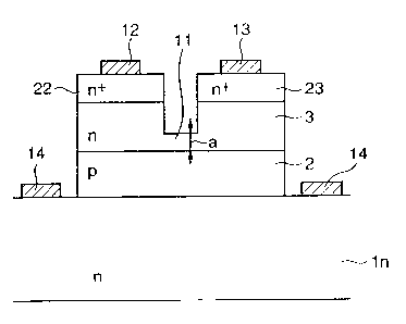
According to another aspect of the present invention there is provided
a transverse junction field effect transistor comprising~
an n-type SiC substrate (ln);
a p-type SiC film (2) formed on the right face of said n-type SiC substrate;
an n-type SiC film (3) including a channel region (11), formed on said p-type
SiC film;
-31-
CA 02689613 2009-12-30
source and drain regions (22, 23) formed on said n-type SiC film separately
on both sides of said channel region respectively; and
a gate electrode (14) provided in contact with said n-type SiC substrate.
According to a further aspect of the present invention there is provided
a transverse junction field effect transistor comprising*
a SiC substrate (1);
a second conductivity type SiC film (2) formed on said SiC substrate;
a first conductivity type SiC film (3) formed on said second conductivity type
SiC film;
a channel region (11) formed by reducing the thickness of said first
conductivity type SiC film;
a source region and a drain region (22, 23), films consisting of first
conductivity type SiC formed on said first conductivity type SiC film,
separately formed on both sides of the channel region respectively; and
a gate electrode (14), wherein
said gate electrode (14) is formed on a flat region (1) of said SiC substrate
or
a flat region (2) of said second conductivity type SiC film.
According to a further aspect of the present invention there is provided
a transverse junction field effect transistor comprising:
an SiC substrate (1) having a gate electrode (14);
a first SiC film (2) formed on said SiC substrate; and
a first conductivity type second SiC film (3), formed on said first SiC film,
including a channel region (11) reduced in thickness and source and drain
regions holding said channel region from both sides, wherein
said first SiC film (2) consists of a high-concentration impurity region (2a),
provided on a portion located under said channel region (11), having a width
substantially identical to the width of said channel region and a length
smaller than the length of said channel region and containing a second
conductivity type impurity in a higher concentration than the value of the
first conductivity impurity concentration of said channel region and a high-
resistance region (2b, 2c, 20b, 20c, 21b, 21c), other than said high-
concentration impurity region, having high electric resistance.
According to a further aspect of the present invention there is provided
a transverse junction field effect transistor comprising*
an n-type SiC substrate;
a p-type SiC film formed on a front face of said n-type SiC substrate;
- 31a-
CA 02689613 2009-12-30
an n-type SiC film, including a channel region, formed on said p-type SiC
film;
source and drain regions formed on said n-type SiC film separately on both
sides of said channel region respectively; and
a gate electrode provided in contact with said n-type SiC substrate,
wherein n-type impurity concentration included in the n-type SiC substrate
is set to same high level of p-type impurity concentration included in the p-
type SiC film so that current flows in a junction portion between the n-type
SiC substrate and the p-type SiC film when positive voltage is applied to the
gate electrode.
According to a further aspect of the present invention there is provided
a transverse junction field effect transistor comprising:
an SiC substrate;
a second conductivity type SiC film formed on said SiC substrate;
a first conductivity type SiC film formed on said second conductivity type
SiC film;
a channel region formed by reducing the thickness of said first conductivity
type SiC film;
a source region and a drain region formed in films comprising first
conductivity type SiC formed on said first conductivity type SiC film,
separately formed on both sides of the channel region respectively; and
a gate electrode,
wherein said gate electrode is formed on a flat region of said SiC substrate
or a flat region of said second conductivity type SiC film, and
wherein said channel region contains a first conductivity type impurity of a
higher concentration than the impurity concentration of portions of the first
conductivity type SiC film located on both sides of said channel region.
According to a further aspect of the present invention there is provided
a transverse junction field effect transistor comprising:
an SiC substrate having a gate electrode;
a first SiC film formed on said SiC substrate; and
- 3lb-
CA 02689613 2009-12-30
a first conductivity type second SiC film, formed on said first SiC film,
including a channel region reduced in thickness and source and drain regions
holding said channel region from both sides, wherein
said first SiC film consists of a high-concentration impurity region, provided
on a portion located under said channel region, having a width substantially
identical to a width of said channel region and a length smaller than a length
of said channel region and containing a second conductivity type impurity in
a higher concentration than a value of the first conductivity impurity
concentration of said channel region and a high-resistance region, other than
said high-concentration impurity region, having high electric resistance.
Brief Description of the Drawings
Fig. 1 is a sectional view of a transverse JFET according to a first
embodiment of the present invention.
Fig. 2 is a sectional view of a transverse JFET according to a second
embodiment of the present invention.
Fig. 3 is a sectional view of a transverse JFET according to a third
embodiment of the present invention.
Fig. 4 is a sectional view of a comparative JFET for the transverse
JFET according to the third embodiment of the present invention.
Fig. 5 is a sectional view of another transverse JFET according to the
third embodiriment of the present invention.
Fig. 6 is a sectional view of a transverse JFET according to a fourth
embodiment of the present invention.
Fig. 7 is a sectional view of a stage forming an n+ SiC film and
patterning the same by RIE in an intermediate fabrication stage for the
transverse JFET shown in Fig. 6.
Fig. 8 is a sectional view of a stage forming a channel region by RIE
after the stage shown in Fig. 7.
- 31c-
CA 02689613 2009-12-30
Fig. 9 is a sectional view of a stage forming an Ni film for forming
electrodes after the stage shown in Fig. 8.
Fig. 10 is a sectional view of a transverse JFET according to a fifth
embodiment of the present invention.
Fig. 11 is a sectional view of a transverse JFET according to a sixth
embodiment of the present invention.
Fig. 12 is a sectional view of a stage forming an n+ SiC film and
patterning the same by RIE in an intermediate fabrication stage for the
transverse JFET shown in Fig. 11.
Fig. 13 is a sectional view of a stage forming a channel region by RIE
after the stage shown in Fig. 12.
Fig. 14 is a sectional view of a stage forming an Ni film for forming
electrodes after the stage shown in Fig. 13.
Fig. 15 is a sectional view of a transverse JFET according to a
seventh embodiment of the present invention.
Fig. 16 is a sectional view of a transverse JFET according to an
eighth embodiment of the present invention.
Fig. 17 is a sectional view of a stage forming an n+ SiC film and
patterning the same by RIE in an intermediate fabrication stage for the
transverse JFET shown in Fig. 16.
Fig. 18 is a sectional view of a stage forming a channel region by RIE
and ion-implanting an impurity after the stage shown in Fig. 17.
Fig. 19 is a sectional view of a stage forming an Ni film for forming
electrodes after the stage shown in Fig. 18.
Fig. 20 is a sectional view of a transverse JFET according to a ninth
embodiment of the present invention.
Fig. 21 is a sectional view of a transverse JFET according to a tenth
embodiment of the present invention.
Fig. 22 illustrates the relation between an element breakdown
voltage and H.
Fig. 23 is a sectional view of a transverse JFET according to an
eleventh embodiment of the present invention.
Fig. 24 is a sectional vi--w of a transverse JFET according to a
-32-
CA 02689613 2009-12-30
twelfth embodiment of the present invention.
Fig. 25 is a model diagram illustrating an OFF-state in the
transverse JFET shown in Fig. 24;
Fig. 26 is a sectional view of a transverse JFET according to a
thirteenth embodiment of the present invention.
Fig. 27 is a sectional view of a transverse JFET according to a
fourteenth embodiment of the present invention.
Fig. 28 is a sectional view of a transverse JFET according to a
fifteenth embodiment of the present invention.
Fig. 29 is a sectional view of a transverse JFET according to a
sixteenth embodiment of the present invention.
Fig. 30 is a sectional view of a transverse JFET according to a
seventeenth embodiment of the present invention.
Fig. 31 is a sectional view of a transverse JFET according to an
eighteenth embodiment of the present invention.
Fig. 32 is a sectional view of a transverse JFET according to a
nineteenth embodiment of the present invention.
Fig. 33 is a sectional view of a transverse JFET according to a
twentieth embodiment of the present invention.
Fig. 34 is a sectional view of a conventional transverse JFET.
Fig. 35 is a sectional view of another conventional transverse JFET.
Fig. 36 is a sectional view of a stage forming an n-channel layer in an
intermediate fabrication stage for the transverse JFET shown in Fig. 35.
Fig. 37 is a sectional view of a stage forming an Ni film defining a
first layer of a two-layer electrode after the stage shown in Fig. 36.
Fig. 38 is a sectional view of a stage forming an Al film defining a
second layer of the two-layer electrode after the stage shown in Fig. 37.
Fig. 39 is a sectional view of a stage providing a trench between a
gate region and a central portion after the stage shown in Fig. 38.
Best Modes for Carrying Out the Invention
Embodiments of the present invention are now described with
reference to the drawings.
-33-
CA 02689613 2009-12-30
(First Embodiment)
Fig. 1 is a sectional view of a transverse JFET according to a first
embodiment of the present invention. A p-type SiC film 2 is formed on an
n-type SiC substrate 1n, and an n-type SiC film 3 reduced in thickness in a
portion of a channel region 11 is formed thereon. On the n-type SiC film,
n+-type impurity layers defining a source region 22 and a drain region 23
are formed through the channel region 11. A source electrode 12 and a
drain electrode 13 form ohmic contact with the source region 22 and the
drain region 23 respectively. According to this embodiment, gate
electrodes 14 are formed to hold the source and drain regions 22 and 23
therebetween in plane. The feature of the aforementioned structure
resides in the multilayer structure of the n-type SiC substrate/(L)
multilayer junction/p-type SiC filml(G) gate junction/n-type SiC film having
the channel region.
(A) A normally on JFET can perform high-speed switching for high
power with a high yield due to employment of the aforementioned structure.
(B) On the other hand, a normally off JFET is so structured that the
thickness of a depletion layer exceeds the thickness a of the channel due to
spreading of the width of the depletion layer toward the n-type SiC film
resulting from a built-in potential in the aforementioned p-n junction.
Therefore, the n-type impurity concentration of the n-type SiC film 3
including the channel region is set to 1 x 1016 cm-3, and the thickness a of
the channel is set to not more than 500 nm, for example. This operation of
the normally off JFET is performed as follows:
(B-1): When the JFET is off, i.e., when the potentials of the gate
electrodes are zero, a diffusion voltage is applied to the gate junction to
form a depletion layer. In this junction, the impurity concentration of the
p-type SiC film is increased for suppressing the depletion layer in
application of a reverse bias voltage to the (L) multilayer junction. Thus,
the impurity concentration is set higher than the n-type impurity
concentration in the channel region as a matter of course, and hence the
depletion layer widely extends toward the channel region with a small
width of extension toward the p-type SiC film. Thus, the depletion layer
- 34 -
CA 02689613 2009-12-30
can block only the channel region by adjusting the impurity concentration.
Consequently, the OFF-state is implemented.
(B-2): When the JFET is on, i.e., when the gate voltage is plus, a
forward bias voltage is applied to the (G) gate junction, no depletion layer
is
formed, and the ON-state is implemented. When the potentials of the gate
electrodes are plus, a reverse bias voltage is applied to the aforementioned
(L) multilayer junction. However, both of the p-type impurity
concentration of the p-type SiC film and the n-type impurity concentration
of the n-type SiC substrate are so increased that the width of a depletion
layer is small and a current flows due to tunneling. As to the
aforementioned high impurity concentrations, the n-type impurity
concentration of the n-type SiC substrate ln is set to about 1 x 1019 cm-3,
and the p-type impurity concentration of the p-type SiC film is set to about
1 x 1019 cm-3. Since the impurity concentrations are increased as described
above, the withstand voltage on the junction may be so reduced that
withstand voltage disappears to allow a current flow. Therefore, the
depletion layer in the aforementioned junction hardly influences on on-off
action of the JFET.
According to the structure of the transverse JFET in the
aforementioned first embodiment, a high-power JFET having a high
switching speed can be prepared with a high yield by employing electros
having high mobility as carriers in the channel region while employing an
n-type SiC substrate having low defect density. The yield of the JFET
according to the aforementioned embodiment in a prototype stage was as
follows: For the purpose of comparison, the yield of a conventional JFET
is also shown.
Inventive Sample: preparation on an n-type SiC substrate (first
embodiment): yield 90 %
Conventional Sample: preparation on a p-type SiC substrate: yield
10%
From the aforementioned results, it is understood that the yield of
the JFET according to this embodiment is remarkably improved.
(Second Embodiment)
-35-
CA 02689613 2009-12-30
Fig. 2 is a sectional view showing a transverse JFET according to a
second embodiment of the present invention. This embodiment is
remarkably different from the JFET according to the first embodiment in a
point that a gate electrode 14 is arranged on the back side of an n-type SiC
substrate in. Operation and functions relevant to the remaining parts are
identical to the operation and functions shown in the first embodiment.
According to this embodiment, the gate electrode 14 is arranged on the back
side of the n-type SiC substrate, whereby a channel region 11 can be
linearly and widely seen through from the gate electrode 14 to the front
face. Therefore, a signal applied to the gate electrode is linearly and
widely transmitted to the channel region, whereby the JFET can perform
on-off action at a high speed. In other words, the JFET can implement a
high-speed switching element. Further, the planar size is reduced in the
JFET according to the second embodiment as compared with the
arrangement of the gate electrodes in the first embodiment, to exhibit
stereoscopic arrangement. Thus, the degree of integration of the JFET can
be improved.
(Third Embo(hment)
Fig. 3 is a sectional view showing a transverse JFET according to a
third embodiment of the present invention. Fig. 4 is a sectional view of a
JFET to be compared therewith. According to this embodiment, an end
face 31 of a p-type SiC film 2 and an end face 32 of an n-type SiC film 3
formed thereon are so misaligned with each other that the former is located
inward beyond the latter in plane. Referring to Fig. 4, on the other hand,
both end faces are formed as aligned end faces 30. In this case, the end
faces 30 are so exposed to ions during RIE that crystals may be damaged
when etched by RIE. In the case of the end face structure shown in Fig. 3,
on the other hand, the end face of the n-type SiC film is etched by first
etching A, while the inner portion is etched and exposed by second etching
B and hence this portion is exposed to an ion atmosphere for only a short
period. Therefore, such a possibihty that crystals around the end face 32
are damaged by ions is extremely reduced. Thus, a JFET having excellent
transistor characteristics can be obtained while ensuring a high yield.
-36-
CA 02689613 2009-12-30
While the JFET shown in Fig. 3 has a back gate structure, a JFET
having a structure arranging gate electrodes 14 on side portions of a
channel is also an influential structure of the present invention. In other
words, a JFET exhibiting a high yield can be obtained without damaging
surface crystals on end portions by employing the structure shown in Fig. 5.
(Fourth Embodiment)
Fig. 6 is a sectional view of a transverse JFET according to a fourth
embodiment. Referring to Fig. 6, a p+-type SiC film 2 is formed on an SiC
substrate 1. The SiC substrate 1 and the p+-type SiC film 2 may be either
of 6H or of 4H. An n-type SiC film 3 formed with a channel region is
formed on the aforementioned p+-type SiC film 2. The n-type SiC film 3 is
reduced in thickness at the center, for defining the channel region 11. A
source electrode 12 and a drain electrode 13 are formed on a source region
and a drain region, which are n+-type SiC films 4 located above both side
portions of the channel respectively. Ends of the p+-type SiC film 2 are not
covered with the upper n-type SIC film 3 but two gate electrodes 14 are
formed on the uncovered relatively wide single plane to hold the source
electrode 12 and the drain electrode 13 formed above the center
therebetween. In other words, conductive paths between the source and
drain regions and the gate electrodes have no portions narrowly necked by
trenches or the like partway but communicate with each other with wide
sections. The n-type impurity concentrations of the source region and the
drain region are set high to attain ohmic contact with Ni or the li_ke. The
impurity concentrations of the respective regions are preferably set as
follows, for example:
The channel region 11 and the n-type SiC film 3: n-type impurity 2 x
1017 cm-3
The source and drain regions (n+-type SiC films) 4: n-type impurity >
1 x 1019 cm-3
The p+-type SiC film 2: p-type impurity > 1 x 1019 cm-3
As to the channel region, the thickness a, the length L and the width
w in a direction perpendicular to the plane of Fig. 6 can be decided in
response to the size of the element. All of the source electrode 12 and the
-37-
CA 02689613 2009-12-30
source region 22, the drain electrode 13 and the drain region 23 and the
gate electrodes 14 and the p+-type SIC film 2 defining the gate region are
connection of high-concentration regions having impurity concentrations
exceeding 1 x 1019 cm-3 and metal films, and hence ohmic contact can be
formed by employing Ni as the material for the metal films, for example.
In order to attain an OFF-state, a reverse bias voltage is applied to
the gate electrodes 14 for extending a depletion layer from a p-n junction
under the channel region 11 toward the channel region 11 and blocking the
section of the channel region. In a broad way, gate resistance Rg is formed
between the gate electrodes and the lower end of the center of the depletion
layer, and the capacitance of the depletion layer can be regarded as the
gate capacitance Cg. In order to attain an ON-state, the reverse bias may
be canceled for eliminating the depletion layer. In the ON-state, carriers
flow from the source electrode toward the drain electrode through the
channel region 11. When repeating on-off action, the aforementioned gate
resistance Rg and the gate capacitance Cg can be regarded as serially
connected, and a rise (fall) time is proportionate to RgCg, which is the time
constant in a transient phenomenon of this circuit. Therefore, the rise
(fall) time in switching can be reduced by reducing the gate resistance Rg.
When the structure of the transverse JFET shown in Fig. 6 is
employed, a JFET having stable performance can be provided by improving
withstand voltage without increasing on-state resistance and reducing a
switching response time. This JFET, providing simple and easy
fabrication steps and hardly causing trouble such as reduction of the yield,
can be fabricated at a low cost as a result.
(Example Corresponding to Fourth Embodiment)
A transverse JFET employing the structure shown in Fig. 6 was
fabricated. In the channel region 11, the channel length L was set to 10
m, the channel thickness a was set to 300 nm (0.3 m), and the channel
width w perpendicular to the plane of Fig. 6 was set to 700 m. Figs. 7 to
9 are diagrams illustrating inventive steps corresponding to Figs. 36 to 39
illustrating the method of fabricating the conventional transverse JFE'1".
First, a p+-type SiC film is formed on a p-type SiC substrate by a
-38-
CA 02689613 2009-12-30
thickness of 1 m, followed by formation of an n-type SiC film. An n+-type
SiC film is further formed thereon followed by etching by RIE, for
patterning a region including source and drain regions. The center of the
portion including the source and drain regions is etched by RIE for
providing a trench thereby isolating the source region 22 and the drain
region 23 from each other (Fig. 8). Further, the gate electrodes are
provided on the p+-type SiC film 2, while the source electrode 12 and the
drain electrode 13 are provided on the source region 22 and the drain
region 23 which are n+ impurity regions respectively (Fig. 9). Thereafter
no etching step is provided for providing trenches in the p+-type SiC film 2.
In the comparative transverse JFET, impurity concentrations were not
particularly increased in both of the source region and the drain region but
left at the concentration of 2 x 1017 cm-3 of the n-type SiC film 3, as shown
in Fig. 35. A transverse JFET setting the depth of the trenches in the p-
type SiC film shown in Fig. 35 to 0.7 m and setting the thickness of p-type
SiC film remaining on the bottom portion to 0.3 m was also prototyped as
comparative example.
Rise (fall) times in switching were measured as to both transverse
JFETs. Table 1 shows results of measurement normalizing the rise time
in comparative example to 1.
Table 1
Transverse JFET Structure Rise (Fall) Ratio
(trenched: 1)
Untrenched (Inventive Example) 0.33
Trenched (Comparative Example) 1
As shown in Table 1, it was possible to reduce the switching rise
(fall) time to 1/3 by forming the p-type SiC film 2 as an untrenched smooth
plane and forming the gate electrodes 14 thereon. Consequently, it has
been rendered possible to obtain a transverse JFET having a high
withstand voltage and low ON-state resistance and capable of high-speed
switching.
(Fifth Embodiment)
-39-
CA 02689613 2009-12-30
Fig. 10 is a sectional view of a transverse JFET according to a fifth
embodiment of the present invention. The impurity concentrations of
portions other than a gate electrode are identical to those of the transverse
JFET shown in Fig. 6. Fig. 10 is characterized in that the gate electrode
14 is formed over the back side of a p-type SiC substrate 1. According to
the structure shown in Fig. 10, ON- and OFF-states can be implemented by
the same manner of applying a gate voltage as that in Fig. 6. Further,
gate resistance Rg can be further reduced, and a rise (fall) time in
switching can consequently be reduced. A fabrication method is also
simplified, and the yield can be improved.
(Sixth Embodiment)
Fig. 11 is a sectional view of a transverse JFET according to a sixth
embodiment. Referring to Fig. 11, a p+-type SiC film 2 is formed on an SiC
substrate 1. On the aforementioned p+-type SiC film 2, a low-
concentration layer 7 containing an n-type impurity of a lower
concentration than a channel region is interposed between an n-type SiC
film and the p+-type SiC film 2 so that there is no portion where these films
3 and 2 are in contact with each other. The channel region 11 is formed on
the said low-concentration layer 7 at the center. A source electrode 12 and
a drain electrode 13 are formed on a source region and a drain region which
are n+ SiC films 4 located above both sides of the channel as viewed from
the channel region respectively. Ends of the p+-type SiC film 2 are not
covered with the upper n-type SiC film 3 but two gate electrodes 14 are
formed on the- uncovered relatively wide single plane to hold the source
electrode 12 and the drain electrode 13 formed above the center
therebetween. In other words, conductive paths between the source and
drain regions and the gate electrodes have no portions narrowly necked by
trenches or the like partway but communicate with each other with wide
sections. The impurity concentrations of the respective regions are
preferably set as follows, for example:
The channel region 11: n-type impurity 2 x 10L7 cm-3
The source and drain regions (n+-type SiC films) 4: n-type inipurity >
1 x 1019 cm-3
-40-
CA 02689613 2009-12-30
The low-concentration layer 7: n-type impurity < 2 x 1017 cm-3
The p+-type SiC film 2: p-type impurity > 1 x 1019 cm-3
As to the channel region, the thickness a, the length L and the width
w in a direction perpendicular to the plane of Fig. 11 can be decided in
response to the size of the element. Except the portions of the electrodes
12, 13 and 14, the face is covered with a protective film 5 consisting of
Si02o
All of the source electrode 12 and the source region 22, the drain electrode
13 and the drain region 23 and the gate electrodes 14 and the p+-type SiC
film 2 defining the gate region are connection of high-concentration regions
having impurity concentrations exceeding 1 x 1019 cm-3 and metal films,
and hence ohmic contact can be formed by employing Ni as the material for
the metal films and performing heat treatment, for example.
Referring to Fig. 11, a forward bias voltage is apphed to the gate
electrodes in an ON-state, and no depletion layer is formed in the channel
region 11. Therefore, carriers flow through a path reaching the drain
region through the source region and the channel region. This path has no
factor increasing ON-state resistance in particular, leading to no power
consumption. When a reverse bias voltage is applied to the gate electrodes
14, a depletion layer extends toward the channel region from a p-n junction
under the channel region and finally completely blocks the channel portion,
for implementing an OFF-state. When no trenches are provided in the p-
type SiC film 2 as in the present invention, gate resistance is so small that
the rise (fall) time is reduced in repetition of this on-off action.
When the structure of the transverse JFET shown in Fig. 11 is
employed, a JFET having stable performance can be provided by improving
withstand voltage without increasing on-state resistance and reducing a
switching response time. This JFET, providing simple and easy
fabrication steps and hardly causing trouble such as reduction of the yield,
can be fabricated at a low cost as a result.
(Example 1 Corresponding to Sixth Embodiment)
A transverse JFET employing the structure shown in Fig. 11 was
fabricated. The structures of respective regions of portions excluding the
channel region 11 and the low-concentration layer 7 are as described above..
-41-
CA 02689613 2009-12-30
In the channel region 11, the channel length L was set to 10 m, the
channel thickness a was set to 300 nm (0.3 m), and the channel width w
perpendicular to the plane of Fig. 11 was set to 700 m. The impurity
concentration of the low-concentration layer (n-impurity layer) was set to 1
x 1015 cm-3, and the thickness was set to 0.1 m.
Figs. 12 to 14 are diagrams illustrating a method of fabricating the
inventive transverse JFET corresponding to Figs. 36 to 39 illustrating the
method of fabricating the conventional transverse JFET. First, a p+-type
SiC film 2 is formed on a p-type SiC substrate 1 followed by formation of a
low-concentration n-type SiC film 7, and an n-type SiC film 3 is formed
thereon. Further, an n+-type SiC film 4 is formed thereon, followed by
etching by RIE, for patterning a region including source and drain regions
(Fig. 12). The center of the portion including the source and drain regions
is etched by RIE for providing a trench thereby isolating the source region
22 and the drain region 23 from each other (Fig. 13). Further, the gate
electrodes are provided on the p+-type SIC film 2, while the source electrode
12 and the drain electrode 13 are provided on the source region 22 and the
drain region 23 which are n+ impurity regions respectively (Fig. 14).
Thereafter no etching step is provided for providing trenches in the p+-type
SiC film 2. A transverse JFET having the structure shown in Fig. 35 was
also prepared for the purpose of comparison. In the comparative
transverse JFET, impurity concentrations were not particularly increased
in both of the source region and the drain region but left at the
concentration of 2 x 1017 cm-3 of the n-type SiC film 3. Table 2 shows
results of measurement of withstand voltages and ON-state resistance
values as to these two transverse JFETs.
-42-
CA 02689613 2009-12-30
Table 2
Withstand ON-State
Transverse JFET Structure Voltage Resistance
(V) (m 4 -cm2)
With Low-Concentration Layer 250 8.7
_
(Inventive Example)
With No Low-Concentration Layer 250 10.0
(Comparative Example)
As shown in Table 2, it was possible to reduce the ON-state
resistance from 10 mS.2.cm2 to 8.7 mS2=cm2 while keeping a high withstand
voltage of 250 V.
(Example 2 Corresponding to Sixth Embodiment)
The structure of the aforementioned transverse JFET according to
the sixth embodiment was employed for measuring the rise (fall) time upon
voltage application as the index of a response speed of a switching eleinent
while varying only the p-type impurity concentration of the p-type SiC film.
Ni films were employed for the electrodes for forming ohmic contact
between the p-type impurity region and the electrodes. Table 3 shows
the results of measurement.
Table 3
Impurity Concentration of
Rise (Fall) Time (ns)
P-Type SiC Film (/cm3).
1 x 10¹⁸ 2000
1x10¹⁹ 200
1 x 10²⁰ 20
1x10²¹ 2
As shown in Table 3, the p-type impurity concentration and the
aforementioned rise time are in inverse-proportional relation, and the ri.se
(fall) time tends to be reduced as the p-type impurity concentration is
increased.
(Seventh Embodiment)
Fig. 15 s a sectional view of a transverse JFET according to a
-43-
CA 02689613 2009-12-30
seventh embodiment of the present invention. Fig. 15 is characterized in
that a gate electrode is formed over the back side of a p-type SiC substrate.
According to the structure shown in Fig. 15, gate resistance Rg can be
reduced, and a rise (fall) time in switching can be reduced as a result.
Further, a fabrication method is also rendered simple and easy, for
improving the yield.
(Eighth Embodiment)
Fig. 16 is a sectional view of a transverse JFET according to an
eighth embodiment of the present invention. Referring to Fig. 16, a 6H-p+-
type SiC film 2 is formed on a 6H-SiC substrate 1. A 4H-type substrate
can be employed in place of the 6H-type substrate, as a matter of course.
"6H-" or "4H-" is omitted in the following description. Referring to Fig. 16,
a channel region 11 contains an n-type impurity in a higher concentration
than the impurity concentration of portions of an n-type SiC film 3 located
on both sides thereof. A source electrode 12 and a ch=ain electrode 13 are
formed on a source region and a drain region which are n+ SiC films 4
located above both sides of the channel as viewed from the channel region
11 respectively. Ends of the p+-type SiC film 2 are not covered with the
upper n-type SiC film 3 but two gate electrodes 14 are formed on the
uncovered relatively wide single plane to hold the source electrode 12 and
the drain electrode 13 formed above the center therebetween. In other
words, conductive paths between the source and drain regions and the gate
electrodes have no portions narrowly necked by trenches or the like
partway but communicate with each other with wide sections. The
impurity concentrations of the respective regions are set as follows, for
example:
The channel region 11: n-type impurity > 1 x 1018 cm-3
The portions of the n-type SiC film 3 located on both sides of the
channel region: n-type impurity 2 x 1017 cm-3
The source and drain regions (n+-type SiC films) 4: n-type impurity >
1 x 1019 cm-3
The p-type SiC film 2: p-type impurity > 1 x 1019 cm-3
As to the channel region, the thickness a, the length L and the width
-44-
CA 02689613 2009-12-30
w in a direction perpendicular to the plane of Fig. 16 can be decided in
response to the size of the element. The source electrode 12 and the source
region 22 as well as the drain electrode 13 and the drain region 23 are
connection of high-concentration regions having impurity concentrations
exceeding 1 x 1019 cm-3 and metal films, and hence ohmic contact can be
formed by employing Ni as the material for the metal films, for example.
Further, connection between the gate electrodes 14 and the p-type SiC film
2 defining the gate region is also connection of high-concentration regions
having impurity concentrations exceeding 1 x 1019 cm-3 and a metal film,
and hence ohmic contact can be formed by employing Ni as the material for
the metal film and performing heat treatment, for example.
In an ON-state of this transverse JFET, carriers flow through a path
reaching the drain region 23 from the source electrode 12 through the
source region 22 and the channel region 11. In this path, the channel
region has a high impurity concentration despite the small sectional area,
whereby resistance can be reduced, ON-state resistance is reduced, and
power consumption can be reduced. Also when a high current is fed,
therefore, power loss is so small that heat generation can be suppressed.
In order to attain an OFF-state, a reverse bias voltage is applied to the gate
electrodes 14 for forming a depletion layer on an n-type SiC film side of a p-
n junction. This depletion layer remarkably develops on both sides of the
channel region 11 and grows into the channel to block the section of the
path of the channel region as the reverse bias voltage is increased. The
OFF-state is attained when the depletion layer blocks the section of the
path of the channel region.
When this structure of the transverse JFET is employed, a JFET
having stable performance can be provided by improving withstand voltage
without increasing ON-state resistance and reducing the switching
response time. Therefore, the JFET can be employed as a high-power
high-speed switching element having low loss. This JFET, providing
simple and easy fabrication steps and hardly causing trouble such as
reduction of the yield, can be fabricated at a low cost as a result.
(Example Corresponding to Eighth Embodiment)
-45-
CA 02689613 2009-12-30
A transverse JFET employing the structure shown in Fig. 16 was
fabricated. Figs. 17 to 19 are diagrams illustrating steps corresponding to
Figs. 36 to 39 illustrating the method of fabricating the conventional
transverse JFET. First, a p+-type SiC film is formed on a p-type SiC
substrate, followed by formation of an n-type SiC film. The impurity
concentration of this n-type SiC film 3 was set to 1.66 x 1017 cm-3. An n+-
type SiC film is further formed thereon followed by etching by RIE, for
patterning a region including source and drain regions (Fig. 17). Then,
the center of the portion includ.ing the source and drain regions is etched by
RIE for providing a trench thereby isolating the source region 22 and the
drain region 23 from each other. A channel region 11 formed under the
bottom of this trench is doped with an n-type impurity by ion implantation
(Fig. 18). The n-type impurity concentration of the channel region 11 was
set t 1.36 x 1018 cm-3. The channel length L was set to 8 m, the channel
thickness -awas set to 214 nm (0.214 m), and the width w of a direction
perpendicular to the figures was set to 0.72 mm. Further, the gate
electrodes are provided on the p+-type SiC film 2, while the source electrode
12 and the drain electrode 13 are provided on the source region 22 and the
drain region 23 which are n+ impurity regions respectively (Fig. 19).
Thereafter no etching step is provided for providing trenches in the p+-type
SiC film 2. In a comparative transverse JFET, impurity concentrations
were not particularly increased in both of the source region and the drain
region but left at the concentration of 1.66 x 101' cm-3 of the n-type SiC
fihn
3, as shown in Fig. 35. A channel was shaped identically to that of the
aforementioned transverse JFET according to the present invention.
Withstand voltages and ON-state resistance values were measured as to
both transverse JFETs. Table 4 shows the results of measurement in both
JFETs.
-46-
CA 02689613 2009-12-30
Table 4
Withstand Voltage ON-State Resistance
Channel (V) (With Application of 1 V)
(m S2 -cm2)
High-Impurity
Concentration Channel 155 0.93
(Inventive Exam le)
Conventional Channel 155 2.20
(Com arative Exam le)
As shown in Table 4, it was possible to reduce the ON-state
resistance from 2.20 mS2-cm2 to 0.93 mS2.cm2 while keeping a high
withstand voltage of 155 V.
(Ninth Embodiment)
Fig. 20 is a sectional view of a transverse JFET according to a ninth
embodiment of the present invention. The impurity concentrations of
portions other than a gate electrode are identical to those in the transverse
JFET shown in Fig. 16. Fig. 20 is characterized in that the gate electrode
14 is formed over the back side of a p-type SiC substrate 1. According to
the structure shown in Fig. 20, ON- and OFF-states can be implemented by
the same manner of applying a gate voltage as that in Fig. 16. Further,
gate resistance Rg can be more reduced, whereby a rise (fall) time in
switching can be reduced as a result. A fabrication method is also
simplified, and improvement of the yield can be attained.
(Tenth Embodiment)
Fig. 21 is a sectional view of a transverse JFET according to a tenth
embodiment of the present invention. Referring to Fig. 21, the thickness a
of a channel region 21 is rendered smaller than the width of a depletion
layer formed on the side of an n- layer due to a built-in potential (about 2 V
to 3 V) of a p-n- junction. The "width" of the junction part indicates the
thickness in Fig. 21. More specifically, the thickness a of the channel
region is not more than 500 nm when the impurity concentration of the n-
layer is set to 1 x 1016 cm-3. The impurity concentration n of the channel
region is preferably set larger than the concentration n- of the n- layer. In
-47-
CA 02689613 2009-12-30
order to implement an ON-state in the transverse JFET shown in Fig. 21, a
positive potential higher than a source potential is applied to gate
electrodes. The p-n- junction is rendered conductive if the gate potential is
increased beyond the built-in potential, and hence it is meaningless to
increase the gate potential beyond the built-in potential. In other words,
the gate potential may be set to zero in an OFF-state, while the gate
potential may be set to a positive level of about 3 V in the ON-state.
Withstand voltage design as to the transverse JFET shown in Fig. 21
is now described. The JFET is designed to have a withstand voltage of 200
V, and the thickness H of an n-type SiC film 3 shown in Fig. 21 is set to 900
nm. At this time, the withstand voltage is 210 to 220 V, reliably exceeding
200 V, on the basis of the relation between H and the withstand voltage
shown in Fig. 22. When H is 900 nm, the thickness a of the channel
region can be set to 500 nm, and the impurity concentration of the n- layer
providing the thickness of the depletion layer larger than this thickness n
resulting from the built-in potential is not more than about 1 x 1016 cm-3, as
described above. The impurity concentration n of the channel region 11
can be set to 3.8 x 1017 cm-3, which is higher than the impurity
concentration of the n- layer. Thus, a normally off transverse JFET can be
obtained while ensuring withstand voltage. Therefore, a normally off
state can be implemented, power consumption can be reduced and a rotary
machine or the like can be controlled by this transverse JFET with no
countermeasure against breakdown of a gate circuit.
(Eleventh Embodiment)
Fig. 23 is a sectional view of a transverse JFET according to an
eleventh embodiment of the present invention. Referring to Fig. 23, an n-
type SiC film is formed by two layers of lower n- layers 3a and upper ni
layers 3b on both sides of a channel region 21. In order to implement
withstand voltage, high-speed on-off action and a normally off state, thc,
concentration ni of the upper layers and the concentration n2 of the channel
region 11 are preferably higher than n-, and n2 is preferably higher than n-.
Also according to this structure, a normally off transverse JFET can be
obtained similarly to the tenth embodiment while ensuring high-speed on-
-48-
CA 02689613 2009-12-30
off action and withstand voltage at a high level.
In order to attain a withstand voltage of 200 V, the thickness H of
the aforementioned two layers (n- layer/ ni layer) is set to 1200 nm, while
setting the impurity concentrations as follows respectively: The withstand
voltage of 200 V can be ensured for obtaining a normally off transverse
JFET carrying out high-speed on-off action by setting the concentration ni
of the upper n layers to 1 x 10L7 cm-3, the concentration n- of the lower n
layers to 1 x 1016 cm-3, the concentration n2 of the channel region to 3.8 x
10" cm-3 and the thickness a of the channel region to 500 nm.
(Twelfth Embodiment)
Fig. 24 is a sectional view showing a transverse JFET according to a
twelfth embodiment of the present invention. Referring to Fig. 24, a p-
type SiC film 2 is formed on an SiC substrate 1, and an n-type SiC film 3
having a portion of a channel region 11 reduced in thickness is formed
thereon. On portions of the n-type SiC film 3 located on both sides of the
channel region 11, n+-type SiC films 22 and 23 for defining source and
drain regions are formed, and source and drain electrodes 12 and 13 are
further formed on the respective regions. Two gate electrodes 14 are
formed on the p-type SiC film through the source and drain regions in
plane. The maximum feature of this embodiment resides in that an
aluminum film 17 is formed on the channel region. The sectional length of
this aluminum film is smaller than a channel length L, and the aluminum
film is included in the channel region in plane. In other words, the
aluminum film 17 is not in contact with walls on both sides of the channel
region 11.
Operation of this JFET is now described. In an ON-state, carriers
flow through the channel region 11 along the substrate face. When the
aluminum film 17 is arranged on the channel region at this time, a
current flows through a parallel circuit formed by the channel region 11
and the aluminum film 17. When the electric resistance of the aluminum
film is lower by 1 order, for example, as compared with the electric
resistance of the channel region, the current flowing through the aluminum
film 17 is highEr substantially by 1 order than the current flowing through
-49-
CA 02689613 2009-12-30
the channel region. Consequently, the current flowing in the
semiconductor is substantially ignorable, and transistor characteristics
hardly depend on the impurity concentration of the channel region or the
thickness a of the channel region. Consequently, the channel region may
not be doped with an impurity of a high concentration for reducing the
electric resistance thereof but other transistor characteristics can be
ensured with no dispersion while keeping high withstand voltage.
In an OFF-state, on the other hand, a negative potential is applied to
the gate electrodes 14 shown in Fig. 25. Therefore, a depletion layer is
formed on the junction between the p-type SiC film 2 and the n-type SiC
film 3, and the width of the depletion layer spreads toward a side having a
lower impurity concentration substantially in inverse proportion to the
impurity concentration as the absolute value of the negative potential is
increased. When the forward end of the width of the depletion layer
exceeds the thickness a of the channel region 11, the depletion layer blocks
the channel region and hinders passage of the carriers. The aluminum
film 17 is not in contact with the walls on both sides of the channel region
11 as described above, and hence the OFF-state is implemented when the
aforementioned forward end of the width of the depletion layer exceeds the
thickness -a of the channel region.
(Example Corresponding to Twelfth Embodiment)
The JFET shown in the twelfth embodiment of Fig. 24 was
prototyped for measuring channel resistance upon application of I V. This
JFET was prepared as an element having a withstand voltage of 100 V.
The impurity concentration of the n-type SiC films 3 and 4 including the
channel region was set to 4.0 x 1017 cm-3, the channel length L was set to
10000 nm (10 m), and the thickness a of the channel region was set to 230
nm.
-50-
CA 02689613 2009-12-30
Table 5
Channel Resistance
Classification (With Application of 1 V)
Unit : m SZ c m2
Inventive Example 1.6
Conventional Example 7.8
According to the results shown in Table 5, the channel resistance of a
conventional JFET (JFET prepared by removing the aluminum film from
the JFET shown in Fig. 24) having no metal film on a channel region was
7.8 mSZcm2. On the other hand, the channel resistance of the JFET
(inventive sample) according to the twelfth embodiment comprising the
aluminum film was remarkably reduced to 1.6 mS2cm2. Therefore, it has
been recognized that the channel resistance is remarkably reduced due to
the inventive sample. Thus, it was possible to obtain a JFET having small
dispersion between elements with no influence by fluctuation of the
irnpurity concentration of the channel region or the thickness of the
channel region.
(Thirteenth Embodiment)
The transverse JFET according to the aforementioned twelfth
embodiment shown in Figs. 24 and 25 implements a normally on state
where the current flows through the channel region 11 when the gate
voltage is zero. A normally on JFET, having a possibility of not stopping
rotation when employed for controlling a rotary machine or the like and a
gate circuit is broken down, must comprise a mechanism for dealing with
breakdown of the gate circuit. It is troublesome to comprise such a
mechanism, and hence a normally off JFET is desirable. The normally off
JFET is described with reference to a thirteenth embodiment. As shown in
Fig. 26, the maximum feature of this embodiment resides in the following
point: The width of a depletion layer resulting from a built-in potential of
a p-n2 junction, i.e., a depletion layer formed when a gate potential is zero,
is rendered larger than the thickness a of a channel region. When (a)
setting a concentration 112 to 1 x 1016 cm-3 and (b) setting the thickness a
of
-51-
CA 02689613 2009-12-30
the channel region to not more than about 500 nm, for example, the width
of the depletion layer resulting from the built-in potential exceeds the
thickness a of the channel region, so that the normally off JFET can be
obtained.
When employing the aforementioned structure, a normally off JFET
neither reducing withstand voltage nor dispersing characteristics due to
fluctuation of the channel concentration or the like can be implemented.
Consequently, the JFET can be applied to a controller for a large-sized
rotary machine or the like without providing a mechanism for dealing with
breakdown of a gate circuit.
(Fourteenth Embodiment)
Fig. 27 is a sectional view showing a transverse JFET according to a
fourteenth embodiment of the present invention. On a p+-type SiC
substrate, p-type epitaxial SiC films 2a, 2b and 2c adjusted in
concentration in response to regions are formed. A p+ SiC layer 2a is
formed on a high-concentration impurity region located under a channel
region 11, and p- SIC layers 2b and 2c of high electric resistance layers are
arranged on both sides thereof. An n-type epitaxial SiC film is formed
thereon, and a trench 19 defines portions connecting the channel region 11
and source and drain regions 22 and 23. High-concentration n- source and
drain regions 22 an 23 are formed on these portions for implementing
ohmic contact respectively, and source and drain electrodes 12 and 13 are
provided thereon. A gate electrode 14 is provided on the back side of the
high-concentration p+-type SiC substrate, for forming a back gate structure.
The gate electrode is provided on the SiC substrate containing an impurity
in high concentration, since ohmic contact can be obtained. However, the
gate electrode may not necessarily have the back gate structure, but such
gate electrodes may alternatively be provided on portions of the SiC
substrate 1 located on sides of the p- SiC layers 2b and 2c of high electric
resistance layers. When the back gate structure is employed, a power
device improved in degree of integration can be formed. When the gate
electrodes are provided on the portions of the SiC substrate 1 located on
sides of the p- SiC layers 2b and 2c of high electric resistance layers, on
the
-52-
CA 02689613 2009-12-30
other hand, the JFET can be advantageously completed while forming
respective portions on a single face in a fabrication flow for a semiconductor
device such as an LSI chip.
Fig. 27 is characterized in that the length of the p+ SiC layer 2a is
rendered smaller than the length of the channel region, and although the
impurity concentration is high, electric resistance of this high-concentration
impurity region is increased by reducing the sectional area in the thickness
direction. Referring to Fig. 27, it is assumed that the direction
perpendicular to the plane of the figure is the width direction of the
transverse JFET, the longitudinal direction of the channel is the length,
and the direction orthogonal to the plane of lamination is the thickness
direction.
The aforementioned p+ SiC layer 2a of the high-concentration
impunty region may not be provided under the channel region 11 but may
be located on a portion close to the source region 22. The p- SiC layers 2b
and 2c of the high-resistance regions located on both sides thereof have a
low impurity concentration and high resistance, and hence the quantities of
currents leaking from the source and channel regions and penetrating into
the p- SiC layers 2b and 2c are reduced.
When the p+ SiC layer 2a is formed by ion implantation, the
minimum width can be set to about 1 m. Therefore, the resistance of this
p+ SiC layer 2a reaches a large value..
When providing the p+ SiC layer 2a small and reducing the
concentration on both sides thereof as described above, a channel leakage
current following a forward bias can be suppressed as compared with the
prior art. Consequently, reduction of the amplification factor in an ON-
state can be prevented.
(Fifteenth Embodiment)
Fig. 28 is a sectional view showing a transverse JFET according to a
fifteenth embodiment of the present invention. Structures different from
those of the transverse JFET shown in Fig. 27 are only high-resistance
regions under source, channel and drain regions. These high-resistance
regions are provided as n- SiC :ayers 2b and 2c on both sides of a p+ SiC
-53-
CA 02689613 2009-12-30
layer 2a. The n-type impurity concentration of these layers 2b and 2c is
reduced, as a matter of course.
In the case of the aforementioned structure, the resistance of the n-
SiC layers 2b and 2c on both sides of the p+ SiC layer 2a is large similarly
to the fourteenth embodiment. Therefore, currents leaking from the
source and channel regions to a first SiC film are suppressed and reduction
of the amplification factor can be prevented, similarly to the fourteenth
embodiment.
(Sixteenth Embodiment)
Fig. 29 is a sectional view showing a transverse JFET according to a
sixteenth embodiment of the present invention. Structures different from
those of the transverse JFET shown in Fig. 27 are only high-resistance
regions under source, channel and drain regions. These high-resistance
regions are provided as two-stage layers, i.e., p- SiC layers 21b and 21c/n-
SiC layers 20b and 20c on both sides of a p+ SiC layer 2a. A reverse bias
voltage is applied to p--n- junction planes of the high-resistance regions
provided on both sides in an ON-state. Therefore, depletion layers are
formed on the p--n- junction planes shown by arrows in Fig. 29. Thus,
resistance against currents leaking from source and channel regions is
extremely increased, and the aforementioned leakage currents are
remarkably suppressed. The case where depletion layers are formed on
peripheral regions other than a high-concentration impurity region of a
first SiC film so that the electric resistance of high-resistance regions is
extremely increased in an ON-state as in this embodiment is most desirable.
(Seventeenth Embodiment)
Fig. 30 is a sectional view showing a transverse JFET according to a
seventeenth embodiment of the present invention. The structure of the
transverse JFET shown in Fig. 30 is different from that of the transverse
JFET according to the fourteenth embodiment shown in Fig. 27 only in a
point that an n+ SiC substrate 1 is employed as the substrate. In other
words, a p+ SiC layer 2a of a high-concentration impurity region is provided
with the smallest possible length, similarly to the fourteenth embodim.ent.
The n+ SiC substrate 1 is employed as the substrate, whereby a
-54-
CA 02689613 2009-12-30
reverse bias voltage is applied to junction planes between the substrate 1
and p- SiC layers 2b and 2c in an ON-state, and hence depletion layers
grow on the p- SiC layers 2b and 2c. According to this embodiment,
therefore, resistance is extremely increased due to formation of the
depletion layers on both sides of the p+ SiC layer 2a of the high-
concentration impurity region, so that currents leaking from source and
channel regions to a first SiC film can be remarkably suppressed. Also in
the seventeenth embodiment, a case where depletion layers are formed on
high-resistance layers in an ON-state is most desirable.
(Eighteenth Embodiment)
Fig. 31 is a sectional view showing a transverse JFET according to
an eighteenth embodiment of the present invention. The structure of the
transverse JFET shown in Fig. 31 is different from that of the transverse
JFET according to the fifteenth embodiment shown in Fig. 28 only in a
point that an n+ SiC substrate 1 is employed as the substrate. In other
words, a p+ SiC layer 2a of a high-concentration impurity region is provided
with the smallest possible length, similarly to the fifteenth embodiment.
A principle suppressing currents leaking to a first SiC film is also identical
to that in the transverse JFET shown in Fig. 28, and hence description is
omitted.
(Nineteenth Embodiment)
Fig. 32 is a sectional view showing a transverse JFET according to a
nineteenth embodinient of the present invention. The structure of the
transverse JFET shown in Fig. 32 is different from that of the transverse
JFET according to the sixteenth embodiment shown in Fig. 29 only in a
point that an n+ SiC substrate 1 is employed as the substrate. In other
words, a p+ SiC layer 2a of a high-concentration impurity region is provided
with the smallest possible length, similarly to the sixteenth embodiment.
A principle suppressing currents leaking to a first SiC film as well as a
principle forming depletion layers are also identical to those in the
transverse JFET shown in Fig. 29, and hence description is omitted.
(Twentieth Embodiment)
Fig. 33 is a sectional view showiu~ g a transverse JFET according to a
-55-
CA 02689613 2009-12-30
twentieth embodiment of the present invention. Each of the
aforementioned fourteenth to nineteenth embodiments has been assumed
to carry out normally on operation. In other words, it has been assumed
that a gate voltage is set to zero or slightly plus with respect to a source
potential (ground potential in general) for attaining an ON-state. In order
to attain an OFF-state, therefore, a prescribed minus voltage must be
applied to a gate. However, an additional control circuit must be provided
on a normally on JFET as a countermeasure against breakdown, and a
transverse JFET carrying out normally off operation is more preferable.
In other words, it is preferable that a depletion layer grows to a channel
region from a p+ SiC layer 2a to block the channel region when the gate
voltage is zero, for attaining an ON-state when the gate voltage is set to a
prescribed plus level.
Referring to Fig. 33, the concentration of a p+ SiC layer 2 of a high-
concentration impurity region is increased and the n-type impurity
concentration of a channel region 11 is reduced so that a depletion layer 18
blocks the channel region 11 with a gate voltage of zero, i.e., with a built-
in
potential. Therefore, the JFET is turned off with the gate voltage of zero,
and no control circuit may be provided for dealing with breakdown of a gate
circuit. The structure of the transverse JFET shown in Fig. 33 is identical
to the structure of the transverse JFET shown in Fig. 27 except the
aforementioned portion, and hence a mechanism of suppressing currents
leaking from source and channel regions to a first SiC film is identical to
that described in the fourteenth embodiment.
While embodiments and Examples of the present invention have
been described in the above, the embodiments and Examples of the present
invention disclosed in the above are only illustrative, and the scope of the
present invention is not restricted to these embodiments and Examples of
the present invention. The scope of the present invention is shown by
description of the scope of claim for patent, and includes all modifications
within the meaning and range equivalent to the description of the scope of
claim for patent.
According to the present invention, it is possible to obtain a JFET of
-56-
CA 02689613 2009-12-30
SiC employing an n-type SiC substrate bringing a high yield and
comprising a channel region employing electrons having high mobility.
Further, it is possible to provide a transverse JFET of uniform quality
suitable for a high-power semiconductor switching element excellent in
withstand voltage and high-speed property. Further it is possible to
obtain a transverse JFET capable of suppressing currents leaking from
source and channel regions to a first SiC film and preventing reduction of
the amplification factor.
-57-