Note: Descriptions are shown in the official language in which they were submitted.
CA 02689672 2009-12-10
= WO 2008/152616
PCT/1E2007/000056
- 1 -
"Low-Profile Transformer"
Technical Field
The present invention relates generally to the field of electrical
transformers for possible
use in motor drive applications, and, more particularly, to improved low-
profile
transformers that may be mounted on and integrated with a suitable substrate,
such as a
printed circuit board (PCB), containing some transformer components.
Background Art
Van Nostrand's Scientific Encyclopedia defines a transformer as being a device
for
transferring electrical energy from one circuit to another by magnetic
induction, usually
with an accompanying change of voltage. There are no moving parts; nor is
there any
electrical connection between the two circuits (except in the case of an auto-
transformer).
The electrical energy is transferred via the magnetic linkage. The energy-
supplying circuit
is termed the "primary", and the energy-receiving circuit is termed the
"secondary".
Some transformers employ three-dimensional bobbin-wound coils. Others employ
relatively-planar or substantially two-dimensional sheet windings that are
embedded in
various dielectric layers of a printed circuit board. For example, U.S. Pat.
No. 6,353,379
B1 discloses a transformer spanning multiple printed circuit boards. Each
board has a
multi-layer structure. Sheet windings are embedded in the various layers. A
magnetic
core, such as an E-core, may be mounted on the main board. The ostensible
purpose of
the device is to lower the profile of the dc-dc converter.
U.S. Pat. No. 5,990,776 discloses another type of transformer having sheet
windings
embedded in various layers of a multi-layer printed circuit board.
U.S. Pat. No. 4,547,961 discloses a miniaturized transformer having sheet
windings
embedded in various layers of a multi-layer printed circuit board. An E-core
embraces the
windings.
CA 02689672 2009-12-10
WO 2008/152616 PCT/1E2007/000056
- 2 -
These references demonstrate that there is an existing and ongoing need to
provide a low-
profile transformer that utilizes printed circuit board technology, that uses
standardizable
off-the-shelf components to minimize the number of different component parts
in the
assembled transformer, and that may use add-on piggyback boards to selectively
vary the
properties of the transformer.
Summary of the Invention
With parenthetical reference to the corresponding parts, portions or surfaces
of the
disclosed embodiment, merely for purposes of illustration and not by way of
limitation,
the present invention provides an improved transformer, which broadly
includes: a
substrate having first and second surfaces; a first board mounted on the
substrate first
surface; a second board mounted on the substrate second surface; the boards
being
identical to one another and being mounted on the respective proximate
substrate surfaces
as mirror images of one another; each of the boards having a plurality of
dielectric layers
with electrically-conductive sheet windings embedded therein; and cores
operatively
arranged to provide a path for magnetic flux attiibutable to a current in the
some of the
windings.
At least one winding of the first board may be connected in series with at
least one
winding of the second board, and these series-connected windings may form a
part of the
primary windings of the transformer.
At least one winding of the first board may be connected in parallel with at
least one
winding of the second board, and these parallel-connected windings may form a
part of
the secondary windings of the transformer.
At least one winding of the first board and/or the second board may be
independent of all
other windings.
The core may be formed by assembling two core portions. A first of the core
portions may
be arranged proximate the first board, and a second of the core portions may
be arranged
CA 02689672 2009-12-10
= WO 2008/152616
PCT/1E2007/000056
-.3 -
proximate the second board. At least one of the core portions may be E-shaped,
and the
other may be E- or I-shaped, or may have some other shape or configuration.
The substrate may be a printed circuit board, and this printed circuit board
may contain
one or more of the transformer windings.
The first and second boards may be formed by a printed circuit technique. Each
board
may include terminals on a surface thereof that are adapted to electrically
connect at least
one of the windings within such board. In one form, each board has at least
four terminals
that are operatively arranged to allow different voltages to be tapped off the
transformer,
even with a mirrored PCB arrangement. Different windings within a board may be
connected by vias.
At least one winding of the first board is connected to at least one winding
of the second
board by at least one via.
The transformer may possibly further include a third board piggybacked on the
first board
and electrically connected thereto, and may possibly include a fourth board
piggybacked
on the second board and electrically connected thereto. The third and fourth
boards may
be identical to one another, but different from the first and second boards.
The third and
fourth boards are preferably mounted on the first and second boards,
respectively, as
mirror images of one another. Each third and fourth board may have a plurality
of
terminals operatively arranged to allow different voltages to be tapped off
the boards. At
least one winding of the third board may be connected in parallel with at
least one
winding of the first board, and at least one winding of the fourth board maybe
connected
in parallel with at least one winding of the second board. Those knowledgeable
in the art
of transformer design will appreciate that this paralleling results in a lower
effective
winding resistance, hence allowing for an increase in the power throughput of
the
transformer. At least one winding of the third board may be conneeted in
series with at
least one winding of the first board, and at least one winding of the fourth
board may be
connected in series with at least one winding of the second board.
CA 02689672 2014-03-17
63 109-5 10
- 4 -
Each board contains groups of terminations associated with the windings of
that particular
board, and the group of terminations on one board is arranged to provide
adequate voltage
clearance, in accordance with IPC standards, relative to the group of
terminations on the same
board or on an adjacent board.
In another aspect, the invention provides a motor controller incorporating any
transformer as
defined above and power switches, the transformer performing DC/DC step-down
conversion
supplying drivers of the power switches.
In one embodiment, the power switches are Insulated Gate Bipolar Transistor
switches.
In a further aspect the invention provides a motor comprising any motor
controller as defined
above.
Accordingly, the invention may, in some embodiments, provide an improved
transformer.
Some embodiments may provide an improved low-profile transformer that is
suitable for use
in motor drive applications.
Some embodiments may provide a low-profile transformer in which the properties
of the
transformer (e.g., turns, ratio, etc.) may be quickly and easily changed or
modified by
mounting standard components (i.e., third and fourth boards) onto the first
and second boards.
Some embodiments may provide a low-profile transformer in which two identical
add-on
boards may be mounted on the first and second boards as mirror images of one
another.
Some embodiments may provide an improved low-profile transformer in which each
add-on
board has a group of terminals associated with the various windings of that
particular board to
allow a desired voltage, or different voltages, to be tapped off that board.
According to an aspect of the invention, there is provided a transformer,
comprising: a
substrate having first and second surfaces; a first board mounted on said
substrate first
surface; a second board mounted on said substrate second surface; a third
board mounted on
CA 02689672 2014-11-18
' 63109-510
- 4a -
said first board and electrically connected thereto; a fourth board mounted on
said second
board and electrically connected thereto; said first board and said second
board being identical
to one another and being mounted on the respective proximate substrate
surfaces as mirror
images of one another; each of said boards having a plurality of dielectric
layers with
electrically-conductive sheet windings embedded therein; and a core
operatively arranged to
provide a path for magnetic flux attributable to a current in some of said
windings.
According to another aspect of the present invention, there is provided a
motor controller
comprising a transformer described above or below, and power switches, the
transformer
performing DC/DC step-down conversion supplying drivers of the power switches.
According to still another aspect of the present invention, there is provided
a motor
comprising a controller described above or below.
According to yet another aspect of the present invention there is provided a
transformer,
comprising: a substrate having first and second surfaces; a first board
mounted on said
substrate first surface; a second board mounted on said substrate second
surface; said first and
second boards being identical to one another and being mounted on the
respective proximate
substrate surfaces as mirror images of one another; each of said first and
second boards having
a plurality of dielectric layers with electrically-conductive sheet windings
embedded therein;
said sheet windings being electrically connected; a core operatively arranged
to provide a path
for magnetic flux attributable to a current in said windings; and wherein each
of said first and
second boards has at least three terminals on a surface thereof that are
electrically connected
to at least one winding within such board and that are operatively arranged to
allow different
voltages to be tapped off.
CA 02689672 2014-03-17
63109-510
- 5 -
These and other aspects and advantages will become apparent from the foregoing
and
ongoing written specification, the drawings and the appended claims.
Brief Description of the Drawing Figures
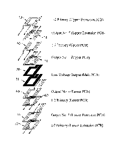
Fig. 1 is-a schematic isometric view showing the first and second boards, and
the
two E-cores, in exploded aligned relation to the main printed circuit board,
Fig. 2 is an enlarged fragmentary longitudinal cross-section of the assembled
transformer that was shown in exploded relation in Fig. 1, and showing the
various layers of each board, the assembled core structure, and the primary
and
secondary windings,
Fig. 3 is a schematic isometric view showing first forms of some of the series-
connected windings within the first and second boards, and showing the first
and
second boards as being arranged as mirror images of one another,
Fig. 4 is a schematic isometric view showing second forms of non-connected
windings within the first and second boards, and showing the first and second
boards as being arranged as mirror images of one another,
Fig. 5 is a schematic isometric view showing third forms of non-connected
windings within the first and second boards, and showing the first and second
boards as being arranged as mirror images of one another,
Fig. 6a is a top plan view of the top layer of the first board, showing the
termirials
of the primary and secondary windings spatially arranged about the PCB,
Fig. 6b is a view of the embedded winding within the second layer from the top
of
the first board, this being part of the primary winding,
CA 02689672 2009-12-10
' WO 2008/152616 PCT/1E2007/000056
- 6 -
Fig. 6c is a view of the embedded winding within the third layer from the top
of
the first board, this being part of the primary winding,
Fig. 6d is a view of the embedded winding within the fourth layer from the top
of
the first board, this being part of the primary winding,
Fig. 7a is a view of the embedded winding within the fifth layer from the top
of
the first board, this being a multi-tapped secondary winding,
Fig. 7b is a view of the embedded via arrangement within the sixth layer from
the
top of the 'first board, this being effectively an unused layer of the PCB,
Fig. 7c is a view of the embedded winding within the seventh layer from the
top
of the first board, this being another multi-tapped secondary winding,
Fig. 7d is a bottom plan view of the eighth layer from the top of the first
board
(i.e., the bottom layer), this view showing the terminals leading to the
center taps
and terminations of the secondary windings, and also showing the completion of
the primary winding,
Fig. 8 is a simplified exploded aligned isometric schematic view of the
transformer shown in Fig. 1, and shows the schematic windings of the first and
second boards and the main substrate boards, but without the two E-cores,
Fig. 9 is an exploded aligned isometric schematic view similar to Fig. 1, and
shows the first, second, third and fourth boards, and the two E-cores,
relative to
the main board, and
Fig. 10 is an exploded aligned isometric schematic view of the transformer
shown
in Fig. 9.
CA 02689672 2009-12-10
WO 2008/152616 PCT/1E2007/000056
- 7 -
Description of the Preferred Embodiments
At the outset, it should be clearly understood that like reference numerals
are intended to
identify the same structural elements, portions or surfaces consistently
throughout the
several drawing figures, as such elements, portions or surfaces may be further
described
or explained by the entire written specification, of which this detailed
description is an
integral part. Unless otherwise indicated, the drawings are intended to be
read (e.g., cross-
hatching, arrangement of parts, proportion, degree, etc.) together with the
specification,
and are to be considered a portion of the entire written description of this
invention. As
used in the following description, the terms "horizontal", "vertical", "left",
"right", "up"
and "down", as well as adjectival and adverbial derivatives thereof (e.g.,
"horizontally",
"rightwardly", "upwardly", etc.), simply refer to the orientation of the
illustrated structure
as the particular drawing figure faces the reader. Similarly, the terms
"inwardly" and
"outwardly" generally refer to the orientation of a surface relative to its
axis of elongation,
or axis of rotation, as appropriate.
The present invention concerns the design and manufacture of low-profile
transformers
for motor drive applications wherein multiple isolated bias supplies are
required. The
improved transformer may include two or more core portions assembled onto a
main
printed circuit board (PCB), with two identical multi-layered printed circuit
boards being
mounted on the main board. The invention allows, through the novel design of
the add-on
boards, the use of identical planar PCBs, and, secondary PCBs (if desired), to
reduce the
number of different components required during manufacture.
The transformer may advantageously be used in a motor controller as a dc/dc
step-down
transformer supplying the drivers of power switches such as Insulated Gate
Bipolar
Transistors (IGBTs) and also supplying bias requirements to control circuits.
The basic assembly is shown in Fig. 1. In this view, various components of an
improved
transformer, generally indicated at 20, are shown in exploded aligned relation
to one
another. These various components include a main printed circuit board 21
having a
planar upper surface 22 and a planar lower surface 23, a first board 24
adapted to be
CA 02689672 2009-12-10
WO 2008/152616 PCT/1E2007/000056
- 8 -
mounted on the substrate or main PCB board upper surface 22, a second board 25
positioned beneath the main board 21 and adapted to be mounted on main board
second
surface 23, and upper and lower E-cores 26,28, respectively, that are adapted
to embrace
the first and second boards so as to provide a path for magnetic flux
attributable to a
current in some of the transformer windings. The first and second boards 24,
25 are
preferably identical to one another, but are mounted on the respective
proximate substrate
surfaces 22, 23 as mirror-images of one another. The main board 21 is, in
fact, a printed
circuit board having a plurality of embedded sheet windings therein. The first
and second
boards are also manufactured by a suitable printed circuit board technique,
and include a
plurality of dielectric layers with various sheet windings embedded therein,
as discussed
infra. The first and second boards 24, 25 are shown as having a plurality of
terminals,
severally indicated at 29.
Fig. 2 is an enlarged fragmentary longitudinal vertical sectional view of the
transformer
shown in Fig. 1, after assembly. This view again shows the main printed
circuit board 21
as having upper and lower surfaces 22,23, respectively. The first and second
boards 24,
are shown as being mounted on these respective substrate surfaces 22,23,
respectively.
The main printed circuit board 21 is depicted as having a plurality of
dielectric layers.
Two vertically-spaced series-connected low voltage windings, indicated at 30,
31, are
20
disposed within the main printed circuit board. These windings are connected
via vias 32
which lead to terminals 33, 34 on the upper and lower surfaces of the main
printed circuit
board.
As previously noted, the first and second boards are preferably structurally
identical, so as
25 to
minimize the number and type of different components of the transformer, and
are
mounted on the proximate surfaces of the main printed circuit board as mirror-
images of
one another. Each of boards 24, 25 may be formed by a suitable printed circuit
board
technique, and may have a plurality of sheet windings, indicated at 35, 36, 37
and 38,
respectively, arranged within various respective vertically-spaced dielectric
layers.
Various of these windings are connected by vias, severally indicated at 39,
which
terminate in terminals 40 at one surface of the associated board. In the
accompanying
drawings, numeral 39 refers generally to a via and numeral 40 refers to a
terminal
CA 02689672 2014-03-17
63109-510
- 9 -
connected with that via. That is not to say that all vias are the same, or
that all vias are
connected to the same sheet windings within the associated board.
Fig. 3 is a schematic view of a sheet winding in one board as being series-
connected to
another identical board arranged as a mirror-image of the first. Note that
terminals "2" of
the boards are connected via a via 42 in the main PCB. Thus, a suitable
voltage may be
impressed between terminal "1" of the upper board and terminal "1" of the
lower board, to
cause current to flow in a clockwise direction, spiraling inwardly in the
upper board and
outwardly in the lower board. Thus, Fig. 3 illustrates the two mirror-image
windings
(41, 41) as being series-connected.
Fig. 4 is a schematic view of another arrangement, generally similar to that
shown in Fig.
3, in which an upper winding 43 is arranged as a mirror-image to a lower
winding 43.
These windings have an off-center tap that produces unequal voltages at the
output of the
transformer. Those knowledgeable in the art of transformer design will
appreciate that the
off-center tap arrangements result in different voltages being produced at the
outputs of
the top windings in comparison to those produced at the outputs of the bottom
winding
due to the fact that the windings are mirrored. Terminals "1" and 113" of the
winding
shown in Fig. 4 correspond generally to terminals "1" and "2" in the winding
shown in
Fig. 3. The principal difference is that there is an off-center tap lestifing
to an intermediate
terminal "2". This allows an interim voltage to be tapped off. The interim
voltage tapped
off in the upper winding 43 is not equivalent to the interim voltage tapped
off the lower
winding 43, due to the fact that the tapping is off center.
Fig. 5 is a schematic view of a corrected form of winding shown in Fig. 4. The
upper
= winding makes use of terminals "I", "2" and "4", whereas the lower
winding makes use of
terminals "4", "3" and "1". In other words, terminal "3" is unused in the
upper winding,
and terminal "2" is unused in the lower winding. This arrangement allows
equivalent
voltages to be achieved from upper and lower windings with the additional
taps. Thus, the
additional tap in each winding enables compensation of the off-center tap
combined with
a mirrored PCB.
CA 02689672 2014-03-17
63109-510
- 10 -
Figs. 6 and 7 are schematic views of the eight layers forming the upper board
24. Fig. 6a
is a top plan view of the uppermost layer 45. Layer 45 is shown as having a
plurality of
spaced rectangular terminals, severally indicated at 46, and a plurality of
spaced vertical
round vias, indicated at 48.
Fig. 6b is a schematic view of the sheet winding in the second layer from the
top, this
being immediately beneath the top layer. Note that current may flow from
terminal 50 in a
clockwise direction and may spiral inwardly to a termination 51. A via
communicates the
inner end of the coil shown in Fig. 6b with the inner end of a coil on the
third layer from
the top, as shown in Fig. 6c. Hence, in the third layer, current may spiral
outwardly
toward a terminal 52. Referring now to Fig. 6d, terminal 52 communicates via a
via with
an input terminal 53 on the fourth layer from the top. This terminal is
connected via a
sheet winding that spirals inwardly and terminates at an eutput 54. Terminal
54 is adapted
to communicate via a via with a mirror-image in the arrangement in the lower
board.
Referring to Fig. 7a, the fifth layer from the top of the upper board is shown
as having
another sheet winding that begins at WI input 55 and terminates at an output
56. The input
55 and output 56 on the fifth layer communicate via the vias shown in Fig. 7b
to
terminations on the eighth layer, as shown in Fig. 7d. Taps from this winding
are taken
from vias located at interim points in the winding, and these taps also
communicate with
the terminations on the eighth layer via vias. Another complete winding is
shown on the
seventh layer from the top, as shown in Fig. 7c. This winding spirals inwardly
between an
input 59 and an output 58. This winding also contains several vias spatially
arranged to
provide off-center taps and terminations, as seen in Fig. 7b.
As best shown in Figs. 7c-7d, input 59 communicates with a terminal 60.
Fig. 8 is a schematic view of the assembled transformer. The main PCB is shown
as
having two low-voltage output windings 30, 31. The first board 24 is shown as
having
one half of the primary winding, indicated at 61.1n fact, winding 61 may be
represented
by a plurality of series-connected windings on the various layers of the upper
board. The
upper board is also depicted as having an output winding, indicated at 62,
which may, in
CA 02689672 2009-12-10
' WO 2008/152616 PCT/1E2007/000056
- 11 -
fact, be on multiple layers. The uppermost winding 61 is shown as having
terminals at
positions "1" and "2", and the output winding 62 is shown as having four
output
terminals. The lower board 25 is arranged as a mirror-image of the upper
board, and has a
primary winding 61 and a secondary winding 62, as indicated above.
Referring now to Figs. 9 and 10, the present invention expressly contemplates
that one or
more additional boards, termed third and fourth boards, respectively, may be
mounted on
or "piggybacked" on the first and second boards, respectively, to improve or
extend the
electrical properties of the transformer. In Fig. 9, the assembly is shown in
an exploded
aligned relation.µ The improved transformer, generally indicated at 70, is
shown again as
including a main printed circuit board 21 having upper and lower surfaces 22,
23,
respectively; a first board 24; a second board 25; and upper and lower E-cores
26, 28 of
the core. However, in this form, a third board, generally indicated at 71, is
mounted on the
first board 24, and is embraced by the E-core. Similarly, a fourth board,
generally
indicated at 72, is mounted on the second board 25, and is embraced by E-core
28. The
third and fourth boards 71, 72 are identical to one another, but are mounted
on the first
and second boards, respectively, as mirror-images of one another. These third
and fourth
boards have terminals or groups of terminals that communicate with internal
windings
therein, and can be readily used to expand the capacity of the first and
second boards. For
example, the third and fourth boards might contain additional primary windings
that can
be parallel-connected to the windings of the first and second boards.
Alternatively, the
third and fourth boards may have additional secondary windings that can be
electrically
connected to the secondary windings of the first and second boards.
Alternatively, these
third and fourth boards may have additional secondary windings that increase
the number
of output voltages from the transformer.
Fig. 10 is a schematic view of the structure shown in Fig. 9. The two coils
30, 31 within
the main circuit board 21 are in the center of this view. Above and below the
main circuit
board are representations as to the first and second boards 24, 25,
respectively. These
boards are depicted as having various layers embedded therein. For example,
first board
24 is depicted as having a primary winding 60 and a secondary winding 61.
Similarly, the
second board is depicted as having a primary winding 60 and a secondary
winding 61.
CA 02689672 2014-03-17
63109-510
- 12 -
,
The third and fourth boards are depicted as having additional primary
windings, generally
indicated at 73 and secondary windings, generallyindicated at 74. These
various windings
are adapted to communicate the corresponding windings in the first and second
boards by
their array of terminals and vias connecting these terminals.
Modifications
The present invention expressly contemplates that many different changes and
modifications may be made. For example, while it is presently preferred that
the various
boards be constructive according to printed circuit board techniques, other
types of
constructional techniques might possibly be used. The number of layers is not
deemed
critical. The particular winding patterns are not deemed critical, albeit they
must be
governed by the ultimate end use. As indicated, the third and fourth boards
may be
piggybacked onto the first and second boards, respectively, if desired. The
array of vias
and groups of terminals is considered to be well within the ambit of a person
skilled in
this art.
Therefore, while several forms of the improved transformer have been shown and
described, and several modifications thereof discussed, persons skilled in
this art will
readily appreciate that various additional changes and modifications maybe
made,
as defined and differentiated by the following claims.