Note: Descriptions are shown in the official language in which they were submitted.
CA 02690153 2009-12-08
WO 2008/154404 PCT/US2008/066159
DYNAMIC EAS DETECTION SYSTEM AND METHOD
SPECIFICATION
CROSS-REFERENCE TO RELATED APPLICATIONS
This utility application claims the benefit under 35 U.S.C. 119(e) of
Provisional
Application Serial No. 60/942,873 filed on June 8, 2007 entitled DYNAMIC EAS
DETECTION and whose entire disclosure is incorporated by reference herein.
BACKGROUND OF THE INVENTION
1. FIELD OF INVENTION
This invention relates to dynamically controlled, digitally-phased, multiple
antenna
elements for generating a dynamically enhanced electromagnetic field for
orientation-
independent tag detection and digital synthesis techniques which improves
signal sensitivity of
electronic article surveillance (EAS) systems.
2. DESCRIPTION OF RELATED ART
An electronic article surveillance (EAS) system typically consists of (a)
tags, (b)
interrogation antenna(s), and (c) interrogation electronics, each playing a
specific role in the
overall system performance.
An EAS loop antenna pedestal(s) is typically installed near the exit of a
retail store and
would alarm upon the unauthorized removal of an article from the store, based
on the detection
of a resonating tag secured to the article. The system comprises a transmitter
unit for
generating an electromagnetic field adjacent to the pedestal, and a receiver
unit for detecting
the signal caused by the presence of the resonating tag in the interrogating
field.
Some desired features in EAS include: no blind spot or null region exists in
the
detection zone; the interrogating field be sufficiently strong near the
antenna for detecting the
presence of a resonating tag in noisy environment, but sufficiently weak far
away for
regulatory compliance, and; the detection performance be unaffected by the
orientation of the
resonating tag.
One approach to suppress far field emission is to mechanically twist an O-loop
antenna
180 in the middle to form an 8-loop. However, a detection null is created in
the area near the
intersection of the figure eight crossover due to the magnetic field lines
running in parallel to
the plane of the tag. This causes significantly reduced detection as optimal
detection is
achieved when the magnetic field lines run perpendicular to the plane of the
tag.
Another approach, EP 0 186 483 (Curtis et al.), utilizes an antenna system
that includes
CA 02690153 2009-12-08
WO 2008/154404 PCT/US2008/066159
a first O-loop antenna and a second 8-loop antenna which is coplanar to the
first. In such an
arrangement, a circular-polarized, interrogating field is created when both
antennas are driven
concurrently with a phase shift such that the energy received by the tag is
the same regardless
of its orientation.
A different antenna structure, disclosed in EP 0 579 332 (Rebers), comprises
two-loop
antenna coils, wherein one coil is part of a series resonance circuit and the
other coil is part of
a parallel resonance circuit; the series and parallel resonance circuits are
interconnected to
form an analog phase-shift network which is driven by a single power source.
An equivalent analog phase-shift network is incorporated in EP 1 041 503 (Kip)
that
relates to a phase insensitive receiver for use in a rotary einission field.
Another approach, U.S. Patent No. 6,166,706 (Gallagher III, et al.), generates
a rotating
field comprising of a magnetically coupled center loop located coplanar to an
electrically
driven 8-loop while overlapping a portion or both of the upper and lower 8-
loops. With this
antenna configuration, magnetic induction produces a 90 phase difference
between the phase
of the 8-loop and the phase of the center loop such that a rotary field is
created.
In U.S. Patent No. 6,836,216 (Manov, et al.), the direction of current flow in
four
antenna coils is separately controlled to generate a resultant magnetic field
that is polarized in
some preferred orientations (vertical, perpendicular, or parallel to the exit
aisle) within the
interrogation zone.
A plurality of antenna configurations is described in U.S. Patent No.
6,081,238 (Alicot)
whereby the antennas are phased 90 apart from each other to improve the
interrogating field
distribution.
EAS systems often utilize resonance effects, such as magnetoelastic resonance
(e.g.
acoustomagnetostrictive or AM) and electromagnetic resonance (RF coil tag).
EAS tags
exhibit a second-order response to an applied excitation, and the resonance
behavior is
mathematically described by an impulse response and a frequency response. The
impulse
response and frequency response from a Fourier transform may be used in two
alternative
means of tag interrogation: pulse-listen interrogation and swept-frequency
interrogation.
EAS antennas are electrically small when compared to the wavelength at the
operating
frequency, typically below 10 MHz, and the interrogation zone which is within
the near-field
region, where the inductive coupling dominates. Planar loops are most commonly
used
because of its simplicity and low cost. Tag excitation requires the magnetic
flux to be
2
CA 02690153 2009-12-08
WO 2008/154404 PCT/US2008/066159
substantially tangential to the length of an AM tag and perpendicular to an
inductive coil tag. A
single antenna loop element inevitably generates an uneven interrogation zone
with respect to
tag position and orientation. In practice, at least two antenna elements are
used to switch the
field direction, thus creating a more uniform interrogation zone.
Previous solutions to the orientation problem include either simultaneously
phasing
or sequentially alternating multiple antenna elements.
EP 0 186 483 (Curtis, et al.) discloses an antenna structure (see Fig. 1)
comprising a
figure-81oop (or 2-loop) element 11 and an O-loop (or 1-loop) element 12 that,
when driven
90 out of phase, generates a constantly rotating field. Curtis's antenna
structure is not well
balanced, as the 0 loop generates a significantly larger field than the figure-
8 loop.
EP 0 645 840 (Rebers) proposes an improved structure (see Fig. 2) that uses 2-
loop
element 14 and a 3-loop element 13. The 3-loop also has an advantage over the
1-loop (of Fig.
1) in terms of far-field cancellation, although it was not a concern in both
Curtis's and the EP 0
645 840 (Rebers) inventions. For continuous transmission where the received
signal is in the
form of modulation on the carrier signal, the phase of the received signal is
sensitive to tag
orientation. Synchronous demodulation, or phase-sensitive detection, will not
work well with a
rotating field that in effect constantly rotates the tag. Quadrature receiver
calculation is
required to eliminate the phase-sensitivity.
EP 1 041 503 (Kip) discloses a receiver (see Fig. 3) that addresses the phase-
sensitivity issue.
U.S. Patent No. 6,081,238 (Alicot) discloses an antenna structure (see Fig. 4)
that uses
two adjacent coplanar single loops, where the mutual coupling introduces a
phase-shift of 90 ,
thus creating a relatively null-free detection pattern. A practical issue with
the phase-shift by
means of mutual coupling is that it requires a high Q to induce 90 of phase
shift between the
two loops, leading to excessive ringing for pulse-listen interrogation. Also,
the induced current
on the coupling loop will not have as large amplitude as the current on the
feeding loop, and
the detection pattern will not be uniform for the two loops.
Disclosed in the same patent is a practical implementation (see Fig. 5) that
alternates
phase difference (either in phase or out of phase) between the two loops to
switch field
direction. The received signals from the two loops are shifted 90 for
subsequent mixing.
When the two antenna loops are in phase (during time interval A as shown in
Fig. 6), there is
no far-field cancellation.
3
CA 02690153 2009-12-08
WO 2008/154404 PCT/US2008/066159
Disclosed in the same patent is a solution by dividing the single loop into
four equal-
area elements assigned with phase of 0 , 90 , 180 , and 270 , as shown in Fig.
7.
The aforesaid methods and implementations have their specific issues and
limitations.
Curtis ignores the receiver and far-field cancellation. EP 0 579 332 (Rebers)
uses RC phase-
shifting circuit that not only introduces insertion loss but also causes
resonance problems if
used in a pulse-listen system. Also, RC phase-shifting circuit may not work
well across a
frequency range due to its limited bandwidth. For a pulse-listen system, it is
simpler to
sequentially alternate the 2-loop and 3-loop in terms of transmission and
receiving. Alicot also
uses phase-shifting circuit for quadrature receiver. As for far-field
cancellation, Alicot divides
the single loop into four equal-area elements. As detection performance is
largely dependent
upon the size of each loop element, the four-element antenna with far-field
cancellation will
have reduced detection compared to the two-element antenna without far-field
cancellation.
All references cited herein are incorporated herein by reference in their
entireties.
BRIEF SUMMARY OF THE INVENTION
It is the object of this invention to eliminate the analog phase-shifting
circuit for both
transmission and receiving, thus eliminating the insertion loss and hence
improving the
signal-to-noise ratio. The received signals from each antenna elements are
digitized or
processed using appropriate digital processing techniques.
Another object of this invention to increase the size of the antenna element
while
achieving substantial far-field cancellation for regulatory compliance.
For two elements driven 90 out of phase, the vector summation is not zero in
far field,
as shown in Fig. 8, and an additional far field cancellation technique is
required.
An improved phasing method, of the present invention, are three antenna
elements that,
when driven 120 out of phase, result in zero vector summation in far field,
as shown in Fig. 9.
An electronic article surveillance system is provided which comprises an
antenna
structure including three or more loops each connected to an independent
transmission driver
for generating a corresponding electromagnetic field wherein the transmission
drivers are
arranged to drive the loops in such a way that a vector sum of the
electromagnetic fields of the
independent transmission drivers is null in a far field and wherein no vector
is separated from
another vector by 180 of phase.
A dynamically controlled electronic article surveillance system for detecting
security
tags is provided wherein an array of antenna elements is digitally phased and
actively driven
4
CA 02690153 2009-12-08
WO 2008/154404 PCT/US2008/066159
for concurrent transmission to generate a plurality of electromagnetic fields
having respective
vectors and wherein the system changes the phases between each of the vectors
for interacting
with security tags for effecting tag detection.
BRIEF DESCRIPTION OF SEVERAL VIEWS OF THE DRAWINGS
The invention will be described in conjunction with the following drawings in
which
like reference numerals designate like elements and wherein:
Fig. 1 is a prior art antenna structure as depicted in EP 0 186 483 (Curtis);
Fig. 2 is another prior antenna structure as depicted in EP 0 645 840
(Rebers);
Fig. 3 is a prior art receiver as depicted in EP 1 041 503 (Kip);
Fig. 4 is another prior art antenna structure as depicted in U.S. Patent No.
6,081,238
(Alicot);
Fig. 5 is a functional diagram of the antenna structure of Fig. 4;
Fig. 6 is a timing diagram for activating the antenna structure of Figs. 4-5;
Fig. 7 is a simplified illustration of different antenna element phasings
shown in
U.S. Patent No. 6,081,238 (Alicot);
Fig. 8 is a simplified illustration of a non-zero far-field vector summation;
Fig. 9 is a simplified illustration of a phased method with far field
cancellation of the
present invention;
Fig. 9A depicts a block diagram of the system of the present invention;
Fig. 10 is a high-level view of the direct digital synthesizer according to
the present
invention;
Fig. 11 is a digital phase shift network according to the present invention;
Fig. 12 is a digital up-converter according to the present invention ;
Fig. 13 is the constrained vector summation for substantial far-field
suppression ;
Fig. 14 shows the received signals being digitally processed using a down-
convert;
phase-shift network;
Fig. 15 is a block diagram for generating of a new composite signal computed
as the
square-of-sum of data for a plurality of receive antennas;
Fig. 16 shows a scheme that produces two composite receive signals derived
from an
array of receive antennas using two different sets of phase shifts;
Fig. 17 shows a block diagram for generating a new composite signal computed
using
the sum-of-square operation on data of a plurality of receive antennas;
CA 02690153 2009-12-08
WO 2008/154404 PCT/US2008/066159
Fig. 18 shows a block diagram whereby an array of antenna elements is
dynamically
phased and actively driven for concurrent transmission;
Fig. 19 shows a block diagram whereby an array of antenna elements is
dynamically
phased and combined in the receiver unit to improve detection;
Fig. 20 illustrates a wide aisle detection scheme with dynamic phasing; and
Fig. 21 depicts an exemplary antenna element comprising windings about an
electromagnetic core, such as a ferrite ceramic material.
DETAILED DESCRIPTION OF THE INVENTION
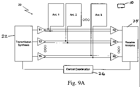
This invention 20 (see Fig. 9A) relates to dynamically controlled electronic
article
surveillance (EAS) systems whereby an array of antenna elements (Ant. 1, Ant.
2... Ant. K) is
digitally phased and actively driven for concurrent transmission 22 and
digitally phased and
then combined in the receiver unit 24 to improve detection of a security tag
10 . All of this is
arranged from a central coordination 26 (e.g., processor). In particular, the
transmit and
receive interrogating field is digitally scanned such that detection may be
reinforced in some
desired locations and still insensitive to tag orientation suppressed in some
other locations. In
one manifestation of the invention, active phasing of multiple antenna
elements for concurrent
transmission is performed digitally using a direct digital synthesizer (DDS).
Fig. 10 shows a high-level view of the DDS 100. A phase delta 101 controlling
the
output frequency is accumulated (i.e., digitally-integrated in time) and
quantized to generate an
index 102 that is mapped by the sine/cosine lookup table 103 to generate the
output RF
waveform 104. After the phase accumulation 105, a desired phase offset 106 is
added to the
result prior to quantization. The phase delta and phase offset can be set or
changed dynamically
in terms of cycles per sample over a wide range of the RF spectrum.
For example, a phase delta of one tenth (1/10) and a phase offset of one
hundredth
(1/100) implies that in 10 time samples, one sinusoid is completed with a
phase shift of
360/100 degree. The DDS output is then presented to a digital-to-analog
converter (DAC) 107
and a low-pass filter 108 to yield the analog, transmit waveform. Different
phase offset
registers are used, one for each antenna element, to produce a digital phasing
network such that
the same lookup table can be time-division multiplexed to produce a plurality
of RF
waveforms. Furthermore, with the availability of both the sine and cosine
outputs from the
same lookup table, a pair of transmit signals are readily generated with a
phase separation of
90 .
6
CA 02690153 2009-12-08
WO 2008/154404 PCT/US2008/066159
In another manifestation of the invention, active phasing of multiple antenna
elements
for concurrent transmission is performed using a digital phase-shift, up-
convert network. A
template in-phase (I) and quadrature (Q) baseband signal is first designed and
presented to a
digital phase shift network followed by a digital up-converter (DUC). Fig. 11
a shows a digital
phase shift network 200 obtained using a network of multipliers and adders to
perform a
plurality of vector rotations according to the rotation matrix
A 45 Ok si11 Ok
Lki. & Ok ,
where [ i, q] represents the template UQ waveform,
n n
akaqk] represents the rotated waveform for antenna element k, and 0 k
represents the phase
shift for antenna element k
Fig. 12 shows a phased shifted output being up-converted in frequency using
the
cascade integrator comb (CIC) up-sampling filter 201 and the DDS 100. The
final up-
converted signal is given according to:
sk (n) = z,ti (n) cos(cvon) - yk (n) sin(mon)
where [ xk , yk ] represents the CIC output for antenna element k
[ cos(won) sin(cvon) ] represents the DDS output, and
COo represents the desired angular frequency of the RF waveform.
The same DDS is employed to perform the frequency up shifting for all of the
transmit antenna
elements. Unlike an analog phase-shift network that is appropriate for use
only at a single (or
narrowband) frequency, the same digital phase shift network 200 (of Fig. 11)
can be used over
a wide range of the RF spectrum simply by adjusting the DDS's phase delta.
In another facet of the invention, to achieve substantial far-field
suppression for
regulatory compliance, the vector summation of the plurality of phase shift
employed to drive
the transmit antenna array must equal zero in the far field. The choice of
phase shifts employed
to drive the transmit antenna array is crucial not only to the pattern of the
interrogating field
generated, but also to the field strength far away from the antenna. In order
that the far-field
energy is suppressed for regulatory purposes, a constraint is imposed here as
shown in Fig. 13
such that substantial far-field suppression is achieved regardless of the
antenna structure and
the number of antenna elements present in the system. For example, in a system
with three
7
CA 02690153 2009-12-08
WO 2008/154404 PCT/US2008/066159
identical antenna elements, if two of the phase shifts were 0 and 120 , then
it would be
desirable to choose a phase shift of 240 for the third antenna element such
that the vector sum
of all phase shifts equals zero.
For another facet of the invention, the plurality of RF/IF receive signals
from the
antenna array are digitally processed using a down-convert, phase-shift
network. The received
RF signal for each antenna is presented to a digital down-converter (DDC)
followed by a
digital phase shifter. Fig. 14 shows a received RF signal being down-converted
in frequency
using the DDS 100 and the CIC down sampling filter 400. The frequency down-
converted
output corresponds to the baseband I/Q signal in a reverse fashion to
operations in the transmit
mode. The same DDS and digital phase shift network used during the transmit
mode are
employed in the receive mode to perform the frequency down shifting and phase
shifting for
all of the receive antenna elements.
For tag detection, a composite receive signal is derived by combining the
plurality of
down-converted, phase-shifted, receive signals using a coherent envelope
detector that
performs the square-of-sum operation. Fig. 15 shows a block diagram for the
generation of a
new composite signal computed as the square-of-sum 500 of data for a plurality
of receive
antennas. For n identical elements, the summation gives a sensitivity that is
n times the
sensitivity of a single element. The effect of the coherent summation is to
rotate and align the
I/Q-vectors from the plurality of receiving antenna elements along the same
direction such that
the resulting vector summation equals the magnitude sum of the induced voltage
on the
receiving antenna elements. By varying the choice of the rotation angles, one
can adjust the
spatial sensitivity or directivity of the receive field as needed to detect a
resonating label at
different spatial coordinate and orientation with respect to the antenna array
structure. This is
particularly appropriate in cases where the mutual coupling between the
antenna elements must
be accounted for. In addition, as the angle of flux line intersection between
the emitted fields
vary continuously in space, the induced voltage on the receive antennas can
have a mutual
phase difference that depends on the location and orientation of the tag.
The invention is also possible of creating, for tag detection, a plurality of
composite
receive signals derived from the many down-converted, phase-shifted, receive
signals using a
coherent envelope detector that performs the square-of-sum 500 operation.
Because the choice
of the phase shifts employed in the receive mode determines the spatial
sensitivity or
directivity of the receive field, different sets of phase shifts may be
required to best detect a tag
8
CA 02690153 2009-12-08
WO 2008/154404 PCT/US2008/066159
entering the interrogating field at different locations, especially when the
signal-to-noise ratio
is poor. Fig. 16 shows a scheme that produces two composite receive signals
derived from an
array of receive antennas using two different sets of phase shifts. The idea
is that while one set
of phase shifting is appropriate for the detection of a resonating tag located
in a specific region,
the other set is appropriate for the detection of the resonating tag located
in a different region.
As another embodiment of the invention, for tag detection, a composite receive
signal
is derived from the plurality of down-converted signals using an incoherent
envelope detector
that performs the sum-of-square operation. Fig. 17 shows a block diagram for
generating a new
composite signal computed using the sum-of-square 700 operation on data from a
plurality of
receive antennas. This corresponds to having a square-law detector (envelope
detector) for
each antenna element and then adding the power (magnitude) from the elements
to get a final
signal measure. For incoherent summation, the implementation is more
straightforward as
compared to coherent summation but the sensitivity being 'Fn, is somewhat less
optimum
compared to n for coherent summation.
The individual frequency and phase of the plurality of transmit signals are
dynamically
altered to allow for automated manipulation (steering) of the transmit field
pattern. With the
use of high-speed computer control (microcontroller, microprocessor, FPGA,
etc) and a phased
array antenna system, the transmit field pattern can be rapidly scanned by
controlling the
phasing and excitation of the individual antenna element. Fig. 18 shows a
block diagram
whereby an array of antenna elements is dynamically phased and actively driven
for concurrent
transmission. A digitally controlled array antenna can give EAS the
flexibility needed to adapt
and perform in ways best suited for tag detection for the particular retail
store environment.
Furthermore, frequency scanning is made possible with the frequency of
transmission changing
at will from time to time. These functions may be programmed adaptively to
exercise effective
automatic management such that the field pattern may be reinforced in some
desired locations
and suppressed in some other locations to localize the detection region.
The individual frequency and phase of the plurality of receive signals are
dynamically
altered to allow for automated manipulation (steering) of the receive field
sensitivity. Fig. 19
shows a block diagram whereby an array of antenna elements is dynamically
phased and
combined in the receiver unit to improve detection. The performance of tag
detection is
affected by the transmit field pattern as well as the receive field
sensitivity due to the law of
reciprocity. In particular, for an EAS system operating in pulsed mode, a
reciprocity exists
9
CA 02690153 2009-12-08
WO 2008/154404 PCT/US2008/066159
between the transmit field intensity and the receive field sensitivity, in
relation to the decay of
field strength as distance increases. Thus, for tag detection, the dynamic
phasing of the
plurality of transmit signals is only effective if dynamic phasing of the
plurality of receive
signals is also performed.
For wide aisle antenna configuration, the antenna elements are arranged to
form a
pedestal pair such that half of the elements having a phase shift of 0~0~ < )r
are located
coplanar on one side of the exit aisle while the other half of the antenna
elements having a
phase shift of lr!!~ oi < 2)r are located coplanar on the other side of the
exit aisle. In particular,
FIG. 20 shows such a scheme 1000 consisting of 4 antenna elements whereby the
0 and 90
loops are arranged in a common plane on one side of the exit aisle, while the
180 and the 270
loops are arranged in a common plane on the other side. Note that the sum of
all the transmit
phases is 360 so that the far-field emission is substantially reduced.
The antenna structures for the dynamic EAS system can be constructed in a
variety of
ways. For instance, rather than being constructed as air-loops, antenna
elements 210 may
consist of windings 206 about electromagnetic cores 204, such as a ferrite
ceramic material,
separated by non-ferrous spacers 202 such as shown in Fig. 21. Distinct loops
may share a
common core or be linearly disposed on adjacent or nearly adjacent segments of
material, or in
a variety of other arrangements.
While the invention has been described in detail and with reference to
specific
examples thereof, it will be apparent to one skilled in the art that various
changes and
modifications can be made therein without departing from the spirit and scope
thereof.