Note: Descriptions are shown in the official language in which they were submitted.
CA 02690750 2013-06-18
Specification
OPTICAL WAVEFORM SHAPING DEVICE
Technical Field
[0001]
The present invention relates to an optical waveform shaping device
and so on.
Background Art
[0002]
The waveform of an optical signal transmitted in an optical
transmission system degrades by ASE noise, non-linear characteristics of an
optical fiber, etc., resulting in degradation of transmission quality. In such
a
case, the degraded waveform of the optical signal is recovered by an optical
waveform shaping device for shaping the waveform an optical signal.
Furthermore, an optical waveform shaping device is used in an observation
device using a femtosecond laser etc., for example, as it is important to
shape a
laser waveform.
[0003]
For example, JP-A 2001-42274 discloses an optical waveform shaping
device with a spatial light modulator for phase modulation and a spatial phase
modulator for intensity modulation. However, the optical waveform shaping
device disclosed in the publication uses two modulators each having a glass
substrate, which inevitably leads to the expansion of the diameter of a beam.
Thus, there is a problem of low resolution.
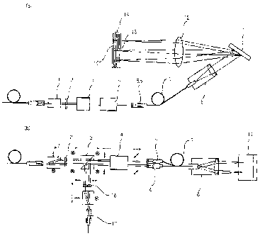
1
CA 02690750 2013-01-18
Patent document 1: JP-A 2003-90926
Patent document 2: JP-A 2002-131710
Brief Description of the Drawings
[0004]
Fig. 1 is a conceptual diagram showing a configuration example of an
optical waveform shaping device of the present invention.
Fig. 2 is a conceptual diagram of a spatial optical modulator having a
phase modulation part and an intensity modulation part.
Fig. 3 is a conceptual diagram showing the orientation of an intensity
modulation part and a phase modulation part.
Figs. 4 are conceptual diagrams for explaining polarization control,
intensity control, and phase control.
Fig. 5 is a diagram showing an example of an optical waveform
shaping device which uses a prism as a folded reflector.
Figs. 6 are figures showing a beam incident on cells. Fig. 6(a) shows a
light beam on the short wavelength side incident on cells, while Fig. 6(b)
shows
a light beam on the long wavelength side incident on cells.
Figs. 7 are figures showing an optical waveform shaping device of the
present invention capable of phase shift compensation. Fig. 7(a) shows an
example using an existing driver, while Fig. 7(b) shows an example performing
DIO direct control.
Fig. 8 is a comprehensive diagram of the optical waveform shaping
device according to Embodiment 1.
Figs. 9 are schematic diagrams of the optical system according to
Embodiment 1. Fig. 9(a) is a top view, while Fig. 9(b) is a side view.
Fig. 10 is a schematic diagram of a simulation determining the
2
CA 02690750 2013-01-18
position of an optical element.
Figs. 11 are figures showing an example of a liquid crystal spatial
light modulator. Fig. 11(a) through Fig. 11(c) are figures showing an overview
of the actually manufactured spatial light modulator.
Figs. 12 are graphs replaced with drawings showing the optical
intensity control characteristic of an optical waveform shaping device. Fig.
12(a) shows a graph of measurement of the optical intensity control
characteristic when an ASE light source is used and all the channels are
controlled collectively. Fig. 12(b) shows a graph of measurement of the
optical
intensity control characteristic when all the channels are intermediately
controlled. Fig. 12(c) shows a graph of measurement of the optical intensity
control characteristic when all the channels are OFF controlled
Figs. 13 are graphs replaced with drawings showing frequency
spacing of an optical waveform shaping device. The wavelength of a
wavelength variable LD light source was swept at a 0.01m step, and the power
of each wavelength with optical intensity controlled was measured with a
power meter. The optical intensity control was set for every 1CH, and the
frequency spacing was checked. Fig. 13(a) shows a frequency spacing in case
of one ON, Fig 13(b) shows a frequency spacing in case of two adjacent ON,
Fig. 13(c) shows a frequency spacing in case of three ON, and Fig. 13(d) shows
a frequency spacing in case of two separate ON.
Fig. 14 shows a graph replaced with a drawing showing the spatial
resolution of an optical waveform shaping device.
Fig. 15 is a schematic diagram showing the device configuration for
measuring an insertion loss.
Fig. 16 is a figure for explaining the optical waveform shaping device
according to the third aspect of the present invention.
3
CA 02690750 2013-01-18
Fig. 17 is a figure for explaining the optical waveform shaping device
according to the third aspect of the present invention.
Description of the Numerals
[0005]
11 Branching filter
12 Condensing part
13 Polarization separation means
14 Spatial light modulator
Disclosure of the Invention
Problems to be Solved by the Invention
[0006]
It is an object of the present invention to provide an optical waveform
shaping device of high resolution.
[0007]
It is an object of the present invention to provide an optical waveform
shaping device of high resolution which is capable of phase shift compensation
associated with optical intensity modulation.
[0008]
It is an object of the present invention to provide an optical waveform
shaping device with a passband generally rectangular in shape. It is an object
of
the present invention to provide an optical waveform shaping device which is
capable of ultrafast optical clock generation of the terahertz order.
[0009]
It is an object of the present invention to provide a band variable
optical waveform shaping device which is capable of miniaturization.
4
CA 02690750 2013-01-18
Means for Solving Problems
[0010]
The present invention is basically based on a knowledge that the use
of a spatial light modulator having a phase modulation part and an intensity
modulation part can provide an optical waveform shaping device of high
resolution, resulting in a new applied technology including ultrafast optical
clock generation of the terahertz order.
[0011]
That is, the first aspect of the present invention relates to an optical
waveform shaping device (10) comprising: a polarization separator (1) for
polarizing/separating the light beam from a light source; a 1/2 wavelength
plate
(2) for joining the polarization planes of a first lightwave and a second
lightwave polarized/separated by the polarization separator (1); a
polarization
beam splitter (3) where the light beams having passed through the 1/2
wavelength plate (2) are incident; a Faraday rotator (4) for rotating in a
predetermined amount the polarization planes of the first lightwave and the
second lightwave having passed through the polarization beam splitter (3); a
first collimator (5) where the lightwave having passed through the Faraday
rotator (4) is incident; a second collimator (6) where the lightwave having
passed through the Faraday rotator (4) is incident; a 2-axis
polarization-preserving fiber (7) where the lightwaves from the first
collimator
and the second collimator are incident; a third collimator (8) where light
beam
having passed through the 2-axis polarization-preserving fiber (7); a
branching
filter (11) for branching the light beam from the third collimator (8) into
the
light beams of each frequency; a condensing lens (12) for condensing the
plurality of light beams branched by the branching filter (11); a polarization
5
CA 02690750 2013-01-18
separation means (13) for adjusting the polarization planes of the light beams
having passed through the condensing lens (12); a spatial light modulator (14)
having a phase modulation part and an intensity modulation part where the
light
beams having passed through the polarization separation means (13) are
incident, the phase modulation part and the intensity modulation part each
having a plurality of liquid crystal cells in a line or in a matrix existing
in the
corresponding spatial positions, the orientation of liquid crystals of the
phase
modulation part being parallel to the polarization plane adjusted by the
polarization separation means (13), the orientation of liquid crystal of the
intensity modulation part being 45 degrees offset from the orientation of
liquid
crystals of the phase modulation part; a prism-type folded reflector (15)
where
the light beams having passed through the liquid crystal spatial phase
modulation and liquid crystal spatial intensity modulation part (14) are
incident; a 1/2 wavelength plate (16) for adjusting the polarization planes of
the
lightwaves output from the polarization beam splitter (3) after having passed
through the folded reflector (15); and a forth collimator (17) where the light
beams having passed through the 1/2 wavelength plate (16) are incident,
wherein the light beam from the third collimator (8) is frequency separated
and
is dispersed spatially by the branching filter (11), wherein the spatially
dispersed and frequency separated light beams are condensed by the
condensing lens (12), wherein the polarization planes of the condensed light
beams are adjusted by the polarization separation means (13), wherein the
light
beams with the polarization planes adjusted are subjected to either or both of
separately controlled phase modulation and intensity modulation by the spatial
light modulator (14), wherein the light beams are folded by the folded
reflector
(15), wherein the light beams are condensed through the condensing lens (12),
wherein the frequency separated light beams are multiplexed by the branching
6
CA 02690750 2013-01-18
filter (11), wherein the lightwave derived from the first lightwave is
incident on
the Faraday rotator (4) through the second collimator (6), wherein the
lightwave derived from the second lightwave is incident on the Faraday rotator
(4) through the first collimator (5), wherein the traveling direction of the
lightwave derived from the first lightwave and the lightwave derived from the
second lightwave having passed through the Faraday rotator (4) are adjusted by
the polarization beam splitter (3), wherein the polarization planes of the two
lightwaves with the traveling direction adjusted are adjusted by the 1/2
wavelength plate (16) so that the polarization planes are orthogonal to each
other, and wherein the lightwaves with the polarization planes adjusted are
output through the forth collimator (17).
[0012]
As demonstrated in the embodiment, the optical waveform shaping
device is an optical waveform shaping device with an extremely high
specification.
[0013]
The preferred embodiment of the first aspect of the present invention
is the optical waveform shaping device wherein the plurality of liquid crystal
cells of the spatial light modulator (14) constitute one channel with two
cells or
three cells depending on the diameter of input light. One channel means a unit
of cell receiving one input light. Specifically, the plurality of liquid
crystal
cells of the spatial light modulator (14) comprise a lattice pitch of 10-40 m,
for
example. Thus, setting the number of cells in view of wavelength dependency
of dispersion characteristic by a branching filter improves the resolution of
wavelength space.
[0014]
The second aspect of the present invention relates to an optical
7
CA 02690750 2013-01-18
waveform shaping device (10) comprising: a polarization separator (1) for
polarizing/separating the light beam from a light source; a branching filter
(11)
for branching a first lightwave and a second lightwave separated by the
polarization separator (1) into the light beams of each frequency; a
condensing
part (12) for condensing the plurality of light beams branched by the
branching
filter (11); a polarization separation means (13) for adjusting the
polarization
planes of the light beam having passed through the condensing part (12); a
spatial light modulator (14) having a phase modulation part and an intensity
modulation part where the light beams having passed through the polarization
separation means (13); and a prism-type folded reflector (15) where the light
beams having passed through the spatial light modulator (14) having the liquid
crystal spatial phase modulation and liquid crystal spatial intensity
modulation
part (14) are incident.
[0015]
Thus, alternating the two optical paths back and forth by a both-sides
telecentric system for the polarized/separated two optical paths can eliminate
the influence on the output by phase change in the polarization/separation
portion.
[0016]
The preferred embodiment of the second aspect of the present
invention relates to the optical waveform shaping device (10) wherein the
first
lightwave and the second lightwave reach the branching filter (11) through a
first axis and a second axis, respectively, of a 2-axis polarization-
preserving
fiber (7) and also the first lightwave and the second lightwave folded through
the reflector (15) are output through the second axis and the first axis,
respectively, of the 2-axis polarization-preserving fiber (7).
[0017]
8
CA 02690750 2013-01-18
Spatial filtering by combining the degradation of the beam quality
derived from the polarization separation control with a 2-axis PM can remove
an irregular change from the intensity distribution of a laser beam. This can
prevent the expansion of the condensing diameter of the beam in the optical
intensity control part and the optical phase control part of the spatial light
modulator (14), resulting in the improvement of resolution.
[0018]
The preferred embodiment of the second aspect of the present
invention is the optical waveform shaping device wherein the plurality of
liquid
crystal cells of the spatial light modulator (14) constitute one channel with
two
cells or three cells depending on the diameter of input light. One channel
means
a unit of cell receiving one input light. Specifically, the plurality of
liquid
crystal cells of the spatial light modulator (14) comprises a lattice pitch of
10-401.im, for example. Thus, setting the number of cells in view of
wavelength
dependency of dispersion characteristic by a branching filter improves the
resolution of wavelength space.
[0019]
In the optical waveform shaping device (10) according to the third
aspect of the present invention, the polarization separation means (13)
comprises a polarization beam splitter (61) and an optical system for guiding
a
first light and a second light separated by the polarization beam splitter
(61) to
the branching filter (11). This configuration allows effective utilization of
the
light beam returning back from the spatial light modulator (14),
polarized/separated and discarded.
[0020]
In the preferred embodiment of the third aspect of the present
invention, the third collimator (8) further comprises a polarization module
(51)
9
CA 02690750 2013-01-18
located at the end face of the 2-axis polarization-preserving fiber (7). And
the
polarization module comprises a first optical system (53, 52, 57) and a second
optical system (56, 54, 55). And the first optical system (53, 52, 57)
controls
the light traveling to the spatial light modulator (14) and the first light
separated by the polarization separation means (13) after having passed
through
the spatial light modulator (14). On the other hand, the second optical system
(56, 54, 55) controls the second light separated by the polarization
separation
means (13).
[0021]
This can improve the insertion loss of 1.5dB derived from the
polarization separation.
Effect of the Invention
[0022]
The optical waveform shaping device of the present invention uses
one spatial light modulator (14) having a phase modulation part and an
intensity modulation part, and the phase modulation part and the intensity
modulation part have a glass substrate in common, which prevents the
expansion of the diameter of a beam, thereby providing high resolution.
[0023]
The optical waveform shaping device of the present invention further
feedbacks the phase shift associated with optical intensity modulation to the
control voltage of liquid crystals, or adjusts the orientation of a polarizer
and
the liquid crystals in the phase modulation part of the spatial light
modulator to
compensate the phase shift associated with intensity modulation, which
compensates the phase shift associated with the optical intensity modulation.
[0024]
CA 02690750 2013-01-18
The optical waveform shaping device of the present invention can
provide an optical waveform shaping device with a passband generally
rectangular in shape as was confirmed in an actual device.
[0025]
The optical waveform shaping device of the present invention can be
used as a band variable optical waveform shaping device as the passbands of
adjacent bands form continuous passbands.
[0026]
The optical waveform shaping device of the present invention can be
miniaturized precisely as optical elements can be omitted and the influences
such as dispersion can be compensated in case it is a reflection type.
Best Mode for Carrying Out the Invention
[0027]
Figs. 1 are conceptual diagrams showing an example of a
configuration of an optical waveform shaping device of the present invention.
Fig. 1(a) is a top view and Fig. 1(b) is a side view. As shown in Fig. 1, the
optical waveform shaping device of the present invention, that is, the first
aspect of the present invention comprises a polarization separator (1) for
polarizing/separating light beam from a light source, a 1/2 wavelength plate
(2)
for joining the polarization planes of a first lightwave and a second
lightwave
polarized/separated by the polarization separator (1), a polarization beam
splitter (3) where the light beams having passed through the 1/2 wavelength
plate(2) are incident, a Faraday rotator (4) for rotating in a predetermined
amount the polarization planes of the first lightwave and the second lightwave
having passed through the polarization beam splitter (3), a first collimator
(5)
where the lightwave having passed through the Faraday rotator (4) is incident,
a
11
CA 02690750 2013-01-18
second collimator (6) where the lightwave having passed through the Faraday
rotator (4) is incident, a 2-axis polarization-preserving fiber (2-PMF (7))
where
the lightwaves from the first collimator and the second collimator are
incident,
a third collimator (8) where light beam having passed through the 2-axis
[0028]
The light from a light source is incident on a polarization separator
12
CA 02690750 2013-01-18
(1) through a single mode fiber etc, for example. The polarization separator
(1)
polarizes/separates the incident light. In this case, the polarization planes
of the
two lights are orthogonal to each other, for example.
[0029]
The first lightwave and the second lightwave polarized/separated by
the polarization separator (1) are incident on a 1/2 wavelength plate (2). The
1/2 wavelength plate (2) rotates either of the polarization planes of the
first
lightwave and the second lightwave polarized/separated by the polarization
separator (1), for example, so that the polarization planes are joined. That
is,
the 1/2 wavelength plate (2) turns the polarization planes of the two
lightwaves
in the same direction.
[0030]
The lightwaves having passed through the 1/2 wavelength plate (2)
are incident on a polarization beam splitter (3). The lightwaves having passed
through the polarization beam splitter (3) are incident on a Faraday rotator
(4).
The Faraday rotator (4) rotates in a predetermined amount the polarization
planes of the first lightwave and the second lightwave having passed through
the polarization beam splitter.
[0031]
The first lightwave having passed through the Faraday rotator (4) is
incident on a first collimator (5), while the second lightwave having passed
through the Faraday rotator (4) is incident on a second collimator (6). Then,
the
lightwaves from the first collimator (5) and the second collimator (6) are
incident on a 2-axis polarization-preserving fiber (7). The lightwaves are
output to the 2-axis polarization-preserving fiber (7) with the polarization
planes maintained. Furthermore, spatial filtering is given by the 2-axis
polarization-preserving fiber (7), resulting in the resolution improvement.
13
CA 02690750 2013-01-18
[0032]
The light beams having passed through the 2-axis
polarization-preserving fiber (7) are incident on a third collimator (8). The
light beam from the third collimator (8) is frequency separated and is
dispersed
spatially by the branching filter (11). The frequency separated and spatially
dispersed light beams after having passed through the branching filter (11)
are
condensed by the condensing lens (12).
[0033]
The polarization planes of the condensed light beams are adjusted by
the polarization separation means (13). The light beams with the polarization
planes adjusted are subjected to either or both of the separately controlled
phase modulation and intensity modulation by the spatial light modulator (14).
[0034]
After the modulation, the light beams are folded by a folded reflector
(15). Then, the folded light beams are condensed through the condensing lens
(12) and are multiplexed by the branching filter (11).
[0035]
The lightwave derived from the first lightwave is incident on the
Faraday rotator (4) through the second collimator (6), while the lightwave
derived from the second lightwave is incident on the Faraday rotator (4)
through the first collimator (5). And, the optical polarization planes are
rotated
in a predetermined amount by the Faraday rotator (4). The polarization beam
splitter (3) adjusts the traveling direction of the lightwave derived from the
first lightwave and the lightwave derived from the second lightwave having
passed through the Faraday rotator (4).
[0036]
A 1/2 wavelength plate (16) adjusts the polarization planes of the two
14
CA 02690750 2013-01-18
lightwaves having passed through the polarization beam splitter (3) so that
the
polarization planes are orthogonal to each other, and the lightwaves with the
polarization planes adjusted are output through a forth collimator (17).
[0037]
The branching filter (11) is an element for branching the light from a
light source into light beams of each frequency. As a branching filter, a
grating,
a prism, or a high-dispersion element such as a grism may be used.
Alternatively, an AWG may be used. As a light source, white light or light
containing a plurality of wavelengths of light, for example, may be used.
Alternatively, pulsed light with a wavelength of approximately 1550nm may be
used. As for the light beam from a light source, the polarizing plane may be
adjusted with a polarization adjuster, a polarizing plate, etc. Furthermore,
the
light beam from a light source may be polarized and separated into two kinds
of
light beams having mutually-perpendicular polarizing planes, for example.
[0038]
The condensing lens (12) serves as a condensing part for condensing a
plurality of light beams condensed by the branching filter (11). A well-known
condensing lens can preferably be used as a condensing lens. The condensing
lens (12) may be provided in the spatial position where the light beams
spatially dispersed by the grating (11) can be condensed and can be guided to
a
predetermined cells of the spatial light modulator (14).
[0039]
The polarization separation means (13) is an optical element for
adjusting the polarization plane of the light beam having passed through the
condensing lens (12). As a polarizing plate, a well-known polarizing plate or
a
polarizer can preferably be used. An interference film type polarizer is more
preferable as the polarizing plate. The use of such an interference film type
CA 02690750 2013-01-18
polarizer indicates the use of a polarizer with a large diameter, which leads
to
improvement of convenience.
[0040]
The spatial light modulator (14) where the light beams having passed
through the polarization separation means (13) is incident has a phase
modulation part and an intensity modulation part each having a plurality of
liquid crystal cells in a line or in a matrix existing in the corresponding
spatial
positions. For example, in the above Patent document 1, a spatial phase
modulation part and a spatial intensity modulation part are separated from
each
other. On the other hand, in the present invention, a phase modulation part
and
an intensity modulation part are joined together and are arranged on a glass
substrate. This can reduce the number of glass substrates used in a spatial
light
modulator to one, which can prevent the expansion of the diameter of a beam,
thereby providing high resolution. In order to control unnecessary reflection,
the phase modulation part and the intensity modulation part are preferably
joined together so that each refractive index is matched. A plurality of
liquid
crystal cells in a line means a plurality of liquid crystal cells arranged in
a
straight line, while a plurality of liquid crystal cells in a matrix means a
plurality of liquid crystal cells arranged in good order vertically and
horizontally. The plurality of liquid crystal cells arranged in a straight
line is
more preferable. And the orientation of liquid crystals of the phase
modulation
part is parallel to the polarization plane adjusted with the polarizing plate
(3),
for example, while the orientation of liquid crystals of the intensity
modulation
part is offset from the orientation of liquid crystals of the phase modulation
part. A specific offset in the orientation of the intensity modulation part is
preferably in the range of 30 degrees-60 degrees, more preferably 40
degrees-50 degrees, most preferably 45 degrees. The liquid crystal spatial
16
CA 02690750 2013-01-18
phase modulation part may exist in the front (the side of the polarization
separation means) of the liquid crystal spatial intensity modulation part, or
the
liquid crystal spatial intensity modulation part may exist in the front.
[0041]
Fig. 2 is a conceptual diagram of a spatial light modulator having a
phase modulation part and an intensity modulation part. As shown in Fig. 2, a
spatial light modulator (14) comprises an intensity modulation part (22)
having
a plurality of liquid crystal cells (21) formed in a line or in a matrix, and
a
phase modulation part (24) having a plurality of liquid crystal cells (23)
corresponding to the liquid crystal cells (21) of the intensity modulation
part.
The liquid crystal cells (21) of the intensity modulation part (22) and the
liquid
crystal cells (23) of the phase modulation part (24) each comprise liquid
crystal
substances as well as electrodes holding the liquid crystal substances
therebetween. This electrode may be a transparent electrode or a metal
electrode existing anywhere in the circumference of the cells. An example of a
specific configuration is such that two liquid crystal elements with a lattice
pitch of 10 m-40tim are joined together and are mounted on a glass substrate.
The lattice pitch is a factor determining the width of each cell. As shown in
Fig.
2, a gap may be provided between the adjacent liquid crystal cells (21,23).
[0042]
Fig. 3 is a conceptual diagram showing the orientation of an intensity
modulation part and a phase modulation part. As shown in Fig. 3, the
orientation of the intensity modulation part is 45 degrees offset from that of
the
phase modulation part, for example. In order for phase modulation and
intensity modulation to be performed with these liquid crystal elements, the
polarization plane by the polarizing plate may be parallel to the orientation
of
liquid crystals of the phase modulation part, and the orientation of liquid
17
CA 02690750 2013-01-18
crystals of the intensity modulation part may be 45 degrees offset from the
polarization plane by the polarizing plate. The offset angle in the intensity
modulation part may be any value except 0 degree. However, 45 degrees is
preferable from a viewpoint of controlling intensity easily.
[0043]
Figs. 4 are conceptual diagrams for explaining polarization control,
intensity control, and phase control. Fig. 4(a) is a diagram showing the
intensity modulation and the phase modulation of the present invention. Fig.
4(b) is a diagram showing the optical phase shift when only the intensity
modulation is performed. As shown in Fig. 4(b), when only the intensity
modulation is performed, intensity is adjusted with an intensity modulator,
and
linear polarization is changed to circular polarization. Then, circular
polarization is changed back to linear polarization with a polarizer. The
intensity modulation is performed in this way. However, as shown in Fig. 4(b),
though the optical phase is back to liner polarization, the phase state is
changed.
On the other hand, as shown in Fig. 4(a), in a system having both intensity
modulation and phase modulation, the phase modulation compensates the phase
shift by the intensity modulation, which allows the phase of output light to
be
matched with the phase of input light.
[0044]
A smaller condensing diameter of the liquid crystal cells on the
condensing lens side is more preferable as it reduces the width of the
obtained
bandpass. From this viewpoint, the condensing diameter may be in the range of
201.1m-80 m, preferably 30 m-70um. And the size of the liquid crystal cells
may be 10p,m-40m, preferably 15 m-30tim, or it may be 151.un-25gm. The use
of such microscopic cells enables the passbands of a 100Hz interval.
Furthermore, as a wavelength becomes larger, the condensing diameter
18
CA 02690750 2013-01-18
becomes larger, and thus one light beam on the short wavelength side may be
received by two liquid crystal cells while one light beam on the long
wavelength side may be received by three liquid crystal cells. The condensing
diameter refers to the diameter of the light beam derived from the image
formed on the liquid crystal cells by a plurality of light beams condensed by
the
condensing lens.
[0045]
A folded reflector (15) is an optical element where the light beams
having passed through a spatial light modulator (14) having a phase modulation
part and an intensity modulation part are incident and shift the traveling
direction. A well-known optical element such as a mirror and a prism can
preferably be used as the folded reflector. This adoption of reflection type
enables the overlapped use of optical elements and also enables compensating
for the influences of dispersion etc., resulting in precise miniaturization of
an
optical waveform shaping device.
[0046]
Fig. 5 is a diagram showing an example of an optical waveform
shaping device which uses a prism as a folded reflector. As shown in Fig. 5,
the
use of a prism (26) can ensure vertical or horizontal optical paths. As a
result,
two kinds of light beams can follow symmetrical optical paths, thereby
equalizing the influences such as a noise derived from the optical paths.
[0047]
Lightwaves are dispersed spatially for each frequency by a grating
(11). The spatially-dispersed lightwaves are condensed with a condensing lens
(12), and are incident on a spatial light modulator (14) through a polarizing
plate (13), where the lightwaves are subjected to separately-controlled phase
modulation and intensity modulation. At the spatial light modulator (14), the
19
CA 02690750 2013-01-18
lightwaves are incident on different cells for each dispersed frequency. Figs.
6
are figures showing a beam incident on cells. Fig. 6(a) shows a light beam on
the short wavelength side incident on cells, while Fig. 6(b) shows a light
beam
on the long wavelength side incident on cells. The cell size is, for example,
a
20gm interval, and the light beam on the short wavelength side may be incident
on two cells, while the light beam on the long wavelength side may be incident
on three cells. Thus, the light beams in real time can be resolved into
frequencies and can be expanded in real space. Furthermore, the number of
cells to a certain beam can be adjusted according to the wavelength dispersion
characteristic of a grating. Light beams are folded by a folded reflector
(15).
The folded light beams are condensed with the condensing lens (12), and the
spatially-dispersed light beams are multiplexed by a branching filter (11).
Thus,
each spatially-dispersed light beam is multiplexed with its phase and
intensity
adjusted.
[0048]
The invention has been explained in the above with reference to a
reflection type optical waveform shaping device. However, the optical
waveform shaping device of the present invention may be a transmission type.
Specifically, a transmission type optical waveform shaping device may
comprise a grating, a first condensing lens, a polarizing plate, a spatial
light
modulator having a phase modulation part and an intensity modulation part, a
second condensing lens, and an optical multiplexer. The same lens as the first
condensing lens may be used as the second condensing lens. The same thing as
the grating may be used as the optical multiplexer.
[0049]
Figs. 7 are figures showing an optical waveform shaping device of the
present invention capable of phase shift compensation. Fig. 7(a) shows an
CA 02690750 2013-01-18
example using an existing driver, while Fig. 7(b) shows an example performing
DIO direct control. In Fig. 7(a), a control device such as a PC is connected
with
a voltage control part (32), and the voltage control part has a SLM driver 1
and
a SLM driver 2 which control the driving voltage applied to a spatial phase
modulation part and a spatial intensity modulation part. On the other hand, in
the case of DIO direct control as shown in Fig. 7(b), the driving voltage
applied
to the spatial phase modulation part and the spatial intensity modulation part
is
directly controlled in accordance with the instructions from the control
device.
As shown in Fig. 7, this optical waveform shaping device comprises a spatial
light modulator (14), a detection part (31), a control device (32), and a
voltage
adjustment part (33). And the control device outputs control signals for
instructing the voltage adjustment part based on the phase shift detected by
the
detection part. On the other hand, the voltage adjustment part outputs
predetermined voltage to the electrode of each cell according to the received
controlled signals. Thus, according to the optical waveform shaping device of
the present invention, the phase shift accompanied with intensity modulation
can be compensated.
[0050]
The detection part (31) is an element for detecting output light from
the optical waveform shaping device when intensity modulation is performed
by an intensity modulation part (22). As the detection part, a well-known
detection device such as a photodiode can arbitrarily be employed. The
detection part (31) is preferably provided within the chassis of the optical
waveform shaping device. Furthermore, the detection part preferably monitors
the controlled variable relating to both optical intensity and optical phase.
[0051]
The control device (32) is a device for receiving information relating
21
CA 02690750 2013-01-18
to the phase shift of each frequency detected by the detection part (31) and
controlling the voltage applied to the electrode of each liquid crystal cell
(23)
of the phase modulation part (24). Specifically, a computer serves as the
control device. The control device may be provided as a unit with the optical
waveform shaping device or may be provided externally. In terms of
downsizing the device, the control device is preferably provided within the
chassis of the optical waveform shaping device. When the detection part
monitors the controlled variable relating to both optical intensity and
optical
phase, such control is preferably performed by a closed loop so that optical
intensity and optical phase come closer to a set value following a comparison
of measured optical intensity and optical phase with the set value. This
control
of optical intensity and optical phase can increase the stability of the
device.
[0052]
The voltage adjustment part (33) outputs the voltage applied to the
electrodes of each liquid crystal cell (23) of the phase modulation part (24)
to
each liquid crystal cell of the phase modulator (24) in accordance with the
control instructions from the control device (32). Furthermore, instead of
feedback control, the orientation direction of a polarizer and the phase
modulation part (24) may be adjusted so that phase modulation can be
performed to compensate the phase shift by intensity modulation. That is, it
is a
preferable mode of the present invention to use the orientation direction of
liquid crystals of a polarizing plane of the polarizer and the phase
modulation
part (24) so that phase modulation can be performed to compensate the phase
shift by intensity modulation. The intensity modulation part may have a
similar
configuration so that the intensity variation accompanied with phase
modulation.
[0053]
22
CA 02690750 2013-01-18
The optical waveform shaping device of the present invention can be
used as a light source for WDM etc. Furthermore, the optical waveform shaping
device of the present invention can be used as an optical transmission device
for EDFA etc.
[0054]
Figs. 16 are figures for explaining the optical shaping device
according to the third aspect of the present invention. Fig. 16A is a figure
for
explaining the first difference with the optical waveform shaping device shown
in Fig. 1. Fig. 16B is a figure showing a polarization module. In the figures,
numeral 51 indicates a polarization module, numerals 52-55 indicate
polarization beam splitters, and numeral 56 and 57 indicate a X/2 wavelength
plate. Numerals 52 and/or 54may be a mirror. In Fig. 16A, the polarization
module is provided at the end face of a 2-axis polarization-preserving fiber
(7)
existing within a third collimator (8). The polarization module may be bonded
to the end face of the 2-axis polarization-preserving fiber (7) with an
optical
adhesive. This configuration provides the third collimator capable of
polarization/separation.
[0055]
Fig. 17 is a figure for explaining the optical waveform shaping device
according to the third aspect of the present invention. As shown in Fig. 17,
the
optical waveform shaping device does not adopt a mere polarizing plate or
polarizer but adopts the configuration shown in Fig. 17 as a polarization
separation means (13). Numerals 61 and 62 indicate polarization beam
splitters,
numeral 64 indicates a V2 wavelength plate, and numeral 65 indicates a
double-sided AR plate. Numeral 62 may be a mirror.
[0056]
Hereinafter, the operation of the optical waveform shaping device
23
CA 02690750 2013-01-18
according to the third aspect of the present invention will be described.
Basic
operations are the same as those of the optical waveform shaping device
according to the first aspect of the present invention. The operations of the
spatial light modulator shown in Fig. 17 will be described. The waveform
shaping device according to the first aspect of the present invention uses a
polarizing plate as a polarization separation means, for example. In this
case, a
part of the polarized/separated light beams will be discarded. On the other
hand,
the optical waveform shaping device according to the third aspect of the
present invention adopts the configuration shown in Fig. 17, and thus the
discarded light beams can be used effectively. That is, as shown in Fig. 17,
the
polarization separation means (13) has a polarization beam splitter (61) as
well
as an optical system for guiding the first light and the second light
separated by
the polarization beam splitter (61) to a branching filter (11). As the first
light
and the second light are polarized/separated by the polarization beam splitter
(61), their polarization planes are different. This configuration allows
effective
utilization of the light returned from the spatial light modulator and then
polarized/separated and discarded. And one example of such an optical system
comprises a polarization beam splitter (61), a polarization beam splitter
(62), a
X/2 wavelength plate (64) and a double-sided AR plate (65). That is, the light
beams returned by a reflector (15) after having passed through the spatial
light
modulator (14) are incident on the polarization beam splitter (61). And the
light
beams incident on the polarization beam splitter (61) are separated to the
first
light and the second light by the polarizing planes. One of the light
separated
travels to a branching filter (11) as in the optical waveform shaping device
according to the first aspect of the present invention. This is called "first
light"
herein. On the other hand, the other light polarized/separated (this is called
"second light" herein) is, after polarized/separated or adjusted its traveling
24
CA 02690750 2013-01-18
direction by the polarization beam splitter (62), incident on the X/2
wavelength
plate (64). Then, the polarizing plane is adjusted by the X/2 wavelength plate
(64). This allows effective utilization of the remaining light
polarized/separated. The optical system for guiding the second light to the
branching filter may be designed arbitrarily (e.g., using a mirror instead of
the
polarization beam splitter (62)).
[0057]
As for the polarization module shown in Fig. 16 preferably has a first
optical system (53, 52, 57) and a second optical system (56, 54, 55). The
first
optical system (53, 52, 57) is an optical system through which the light
traveling to a spatial light modulator (14) and the first light
polarized/separated
through the spatial light modulator (14) pass. The second optical system (56,
54,
55) is an optical system for the second light polarized/separated through the
spatial light modulator (14). The first optical system (53, 52, 57) comprises
a
polarization beam splitter (53) where the light output from the end face of a
2-axis polarization-preserving fiber (7) is incident, an optical element (52)
where one of the light beams polarized/separated by the polarization beam
splitter (53), and a X/2 wavelength plate (57) where the light beams having
passed through the optical element (52). Examples of the optical element (52)
include a polarization beam splitter, a polarizing plate, a polarizer, and a
mirror.
In case the first light polarized/separated through the spatial light
modulator
(14) returns to the polarization module (51), the light passes through the X/2
wavelength plate (57), the optical element (52), and the polarization beam
splitter (53) back to the 2-axis polarization-preserving fiber (7). The second
optical system (56, 54, 55) has a polarization beam splitter (55), and an
optical
element (54) and a X/2 wavelength plate (56). Examples of the optical element
(54) include a polarization beam splitter, a polarizing plate, a polarizer,
and a
CA 02690750 2013-01-18
mirror. The second light polarized/separated through the spatial light
modulator
(14) passes the A./2 wavelength plate (56), the optical element (54), and the
polarization beam splitter (55) in this order back to the 2-axis
polarization-preserving fiber (7). That is, the polarization plane of the
second
light polarized/separated through the spatial light modulator (14) is adjusted
by
the k/2 wavelength plate (56), polarized/separated by the polarization beam
splitters (mirrors) (54, 55) and adjusted its traveling direction, returns to
the
2-axis polarization-preserving fiber (7). This allows bidirectional
operations.
Furthermore, the provision of a number of optical separation means allows
multichannelization.
Embodiment 1
[0058]
Fig. 8 is a comprehensive diagram of the optical waveform shaping
device according to Embodiment 1. Figs. 9 are schematic diagrams of the
optical system according to Embodiment 1. Fig. 9(a) is a top view, while Fig.
9(b) is a side view. In the figures, PBS indicates a polarizing beam splitter,
FR
indicates a Faraday rotator, SMF indicates a single mode fiber, and 2-PMF
indicates a 2-axis polarization-preserving fiber. As shown in Figs. 9, this
optical system comprises a 2-axis polarization-preserving fiber (2-PMF), a
collimating lens with a diameter of 15cm and a focal length of 6cm, a grating
having a surface center position at 6cm from the collimating lens, a
condensing
lens (f15cm) positioned at 15cm from the surface center position of the
grating,
a polarizing plate, a liquid crystal spatial intensity adjustment part, a
liquid
crystal spatial phase modulation part, and a folded reflector. The position of
the
folded reflector (prism) was set at 15cm from the condensing lens. The width
of
the control part of each liquid cell was set 1711m, and the size of the gap
part
26
CA 02690750 2013-01-18
was set 3pm. That is, one cell size was 20gm. The distance between the
collimating lens and the grating and the distance between the collimating lens
and the condensing lens were calculated by doing simulation as shown in Fig.
10.
[0059]
Phases fluctuate sensitively to the changes such as tension or
temperature of a fiber. As this embodiment employs the above configuration,
when the two optical paths of fibers are replaced with each other, the outward
path and the return path will receive the same phase shift in total. As a
result,
though fibers etc. lack phase stability, an optical waveform shaping device
with
high phase stability can be provided.
[0060]
Figs. 11 are figures showing an example of a liquid crystal spatial
light modulator. Fig. 11(a) through Fig. 11(c) are figures showing an overview
of the actually manufactured spatial light modulator. The spatial optical
modulator shown in Fig. 11(a) used a glass substrate with a width of 65mm x
48mm and a thickness of 0.5mm. The size of a liquid crystal cell gap located
between glass substrates having a common electrode and a pattern electrode
respectively was set 8p.m. The width of a liquid crystal lattice was 14 x
14mm,
and it was installed near the center of the glass substrates. The pitch of the
liquid crystal lattice was 20p,m (specifically, the control area was 17tim and
the
gap was 3p,m). As for the orientation of liquid crystals, the orientation
direction
was set 45 degrees in case of intensity control, and it was set 0 degree in
case
of phase control. The liquid crystal spatial light modulator for intensity
control
and the liquid crystal spatial light modulator for phase control were prepared
separately.
[0061]
27
CA 02690750 2013-01-18
In Fig. 11(b), the glass substrate with a width of 65 x up to 30mm and
a thickness of 0.3mm was used. The size of a liquid crystal cell gap located
between glass substrates having a common electrode and a pattern electrode
respectively was set 8 m. The liquid crystal lattice with a size of lOmm x up
to
5mm was used. In Fig. 11(b), the liquid crystal spatial light modulator was
put
to either the left or the right of the glass substrate. This intentional
arrangement
of the liquid crystal light modulator away from the center enabled easier
preparation. As a pitch of the liquid crystal lattice, the following three
patterns
were manufactured:
(i) Pitch of liquid crystal lattice: 201Am (control area: 171.tm, gap: 34m)
(ii) Pitch of liquid crystal lattice: 2012m (control area: 18gm, gap: 211m)
(iii) Pitch of liquid crystal lattice: 10i.tm (control area: 81.tm, gap:
21.tm)
As for the orientation of liquid crystals, the orientation direction was
set 45 degrees in case of intensity control, and it was set 0 degree in case
of
phase control. The liquid crystal spatial light modulator for intensity
control
and the liquid crystal spatial light modulator for phase control were prepared
separately. When connecting the two liquid crystal elements, a marker for
positioning the lattices was provided. Furthermore, control ICs were
collectively arranged on one side of the glass substrate.
[0062]
In the spatial light modulator as shown in Fig. 11(c), a liquid crystal
spatial light modulator for intensity control and a liquid crystal spatial
light
modulator for phase control are provided on each of the surface and the rear
surface respectively of the glass substrate having a pattern electrode. These
were prepared with the potion of the lattices aligned. As shown in Fig. 11(c),
28
CA 02690750 2013-01-18
this liquid crystal spatial light modulator has the configuration where the
glass
substrate having the pattern electrode is put between two substrates having a
common electrode. The size of a liquid crystal cell gap located between glass
substrates each having a common electrode and a pattern electrode was set Sum.
The liquid crystal lattice with a size of up to 20mm x up to 5mm was used. In
Fig. 11(c), the liquid crystal spatial light modulator was put to either the
left or
the right of the glass substrate. This intentional arrangement of the liquid
crystal light modulator away from the center enabled easier preparation. As a
pitch of the liquid crystal lattice, the following three patterns were
manufactured:
(i) Pitch of liquid crystal lattice: 20 m (control area: 17 m, gap: 3 m)
(ii) Pitch of liquid crystal lattice: 20um (control area: 1811m, gap: 21.tm)
(iii) Pitch of liquid crystal lattice: 10um (control area: 8um, gap: 21.tm)
As for the orientation of liquid crystals, the orientation direction was
set 45 degrees in case of intensity control, and it was set 0 degree in case
of
phase control. The liquid crystal spatial light modulator for intensity
control
and the liquid crystal spatial light modulator for phase control were prepared
as
a unit with the glass substrate having a pattern electrode in common.
[0063]
Figs. 12 are graphs replaced with drawings showing the optical
intensity control characteristic of an optical waveform shaping device. Fig.
12(a) shows a graph of measurement of the optical intensity control
characteristic when an ASE light source is used and all the channels are
controlled collectively. Fig. 12(b) shows a graph of measurement of the
optical
intensity control characteristic when all the channels are intermediately
29
CA 02690750 2013-01-18
controlled. Fig. 12(c) shows a graph of measurement of the optical intensity
control characteristic when all the channels are OFF controlled. Fig 12(a)
shows that the passbands of adjacent bands forms continuous passbands in the
optical waveform shaping device of the present invention. On the other hand,
Fig .12(b) shows that the intensity control variable can be set arbitrarily
within
the control range. Fig. 12(c) shows that output can be suppressed in case of
OFF control.
[0064]
Figs. 13 are graphs replaced with drawings showing frequency
spacing of an optical waveform shaping device. The wavelength of a
wavelength variable LD light source was swept at a 0.01m step, and the power
of each wavelength with optical intensity controlled was measured with a
power meter. The optical intensity control was set for every 1CH, and the
frequency spacing was checked. Fig. 13(a) shows a frequency spacing in case
of one ON, Fig 13(b) shows a frequency spacing in case of two adjacent ON,
Fig. 13(c) shows a frequency spacing in case of three ON, and Fig. 13(d) shows
a frequency spacing in case of two separate ON.
[0065]
Fig. 14 is a graph replaced with a drawing showing the spatial
resolution of an optical waveform shaping device. An ASE light source was
used and the optical intensity was controlled for every 48C11 (ON as a whole;
OFF control for every 48CH). The spatial resolution per PAL-SLM cell in each
wavelength band was measured from the control wavelength difference. As a
result, the spatial resolution was 12.1GHz/cell at a wavelength of 1535nm, the
spatial resolution was 10.7GHz/cell at a wavelength of 1550nm, and the spatial
resolution was 9.2GHz/cell at a wavelength of 1565nm.
[0066]
CA 02690750 2013-01-18
Fig. 15 is a schematic diagram showing a device configuration for
measuring an insertion loss. As a result, the insertion loss was 6.5dB at a
wavelength of 1535nm, the insertion loss was 5.0dB at a wavelength of 1550nm,
and the insertion loss was 7.5dB at wavelength of 1565nm.
[0067]
Table 1 is a table showing the dispersion characteristic of a grating.
[Table 1]
Wavelength Incident angle Diffraction angle Diffraction
efficiency
1540nm 50deg 68.9deg 87.0%
1550nm 50deg 70.0deg 88.2%
1560nm 50deg 71.2deg 89.1%
[0068]
Table 2 is a table showing the diameter of a PAL-SLM incident beam.
[Table 2]
Wavelength Condensing diameter (x-axis) Condensing diameter (y-axis)
1530nm (Dx-401.tm 4:Dx ¨ 74 m
1550nm (rox-38tim (Dx-65Rm
1570nm (134x-451.tm (11tx ¨ 86p.m
Industrial Applicability
[0069]
The optical waveform shaping device of the present invention is
preferably used in the fields such as optical information and communication.
31