Note: Descriptions are shown in the official language in which they were submitted.
CA 02692353 2009-12-31
1
DESCRIPTION
DISPLAY-PROTECTIVE PLATE FOR ELECTRONIC APPARATUS
AND ELECTRONIC APPARATUS THEREWITH
Technical Field
The present invention relates to a display-
protective plate for an electronic apparatus that is
attached to a case of an electronic apparatus having a
display such as a liquid crystal display so as to protect a
display surface of the ctisplay, and also add a special
designing effect thereto, and also relates to an electronic
apparatus having such a protective plate.
Background Art
An electronic apparatus having a small-size
display device, such as a portable telephone or a portable
information terminal (PDA) like an electronic notebook,
uses a flat panel display, such as a liquid crystal display,
an organic EL display, an electric field discharge-type
display, or a plasma display, as its display device.
In order to protect the display surface of this
display, a protective plate made from a plastic material,
glass, or the like is bonded to the case of an electronic
apparatus so as to prevent the display surface of the
display from being exposed..
CA 02692353 2009-12-31
2
This protective plate is used not only for
protecting the display surface of the display, but also for
imparting a designing effect to the electronic apparatus.
In particular, in recent years, there have been strong
demands for electronic apparatuses having special designing
features such as metallic gloss, and a protective plate or
the like to which a special- designing feature is added as a
whole, without causing degradation of displaying
performance of the display, has been disclosed.
For example, Patent Document 1 has disclosed a
protective plate for a portable display device in which a
scattering preventive coat film is attached to one of
surfaces of a reinforcing glass plate, with a film with
characters or a pattern printed thereon being attached to
the same surface. Here, in this protective plate, the film
is a so-called frame-shaped member that has characters or a
pattern printed only on the film base portion, with its
center portion being bored, and a double-sided tape used
for bonding the glass plate and the film to each other is
also made of a frame-shaped member having the same shape as
the film. Since the film is molded into a shape having the
bored portion in the center, the display is easily viewed
through a portion other than the printed portion having the
frame shape.
Patent Document 1: JP-A No. 2003-140558
CA 02692353 2009-12-31
3
Disclosure Of Invention
Issues to be Solved by the Invention
In this case, however, since the pattern
concealing the periphery of: the transparent window portion,
disclosed in Patent Document 1, is formed by printing, the
pattern has a low reflective property, and is poor in high-
quality designing effect. Here, in the case when, upon
printing, an aluminum vapor deposition film is formed, the
reflectance can be improved slightly; however, this method
also fails to provide a sufficient high-quality designing
effect.
Moreover, in the center portion where the display
is placed, no film is attached thereto, with the result
that no decoration is pl.aced to cause a limitation in
designing. That is, since the display is always visible
from the outside regardless of the use or no use of the
electronic apparatus, it gives influences on the designing
effect of the surface of the electronic apparatus.
Furthermore, the display to be attached to an
electronic apparatus is ncrmally set to a so-called stand-
by state with no screen display when not used, so as to
reduce power consumption. At this time, when the portion
covering the display has a transmitting property as
described above, the display with no screen display in its
stand-by state is always visible from the outside. This
CA 02692353 2009-12-31
4
state is not desirable for the electronic apparatus from
the designing viewpoint, and, for example, it is not
possible to make the outside appearance different depending
on the power-off state and the stand-by state of the
electronic apparatus.
Therefore, a technical object to be achieved by
the present invention is ta provide a protective plate that
can ensure sufficient visibility of a display, and has a
superior designing effect, and an electronic apparatus
using such a protective plate.
Means for solving the Issues
In order to achieve the above-mentioned technical
object, the present invent_Lon provides a display-protective
plate for an electronic apparatus and an electronic
apparatus using the sarne, which have the following
structures.
According to a first aspect of the present
invention, there is provided a display-protective plate
for an electronic apparatus, which is attached to a case of
an electronic apparatus to be used, and protects a display
surface of a display that is attached to the case so as to
be exposed from the case of the electronic apparatus,
comprising:
a plate-shaped transparent base member;
CA 02692353 2009-12-31
a color half mirror layer that is placed on a
lower side of the transparent base member, and made of a
tint-treated metal thin film;
a transparency-switching film that is placed on a
5 lower face of the color half mirror layer, for switching
between transmitting and non-transmitting modes
electrically;
a transparent reflection-increasing film layer
that is placed on a lower face of the transparency-
switching film, and is a composite film formed by
alternately laminating high refractive-index films and low
refractive-index films; and
a backing layer that is formed on a lower face of
the reflection-increasing film layer in a tightly contact
state without having an a-Lr layer interposed therebetween,
and located on a portion except for an exposed portion of
the display, which are successively laminated.
According to a second aspect of the present
invention, there is provided the display-protective plate
for an electronic apparatus according to the first aspect,
wherein the transparency--switching film is formed by a
polymer dispersion-type liquid crystal film and adapted to
be capable of switching between transparent and white non-
transparent modes upon application of a voltage.
According to a third aspect of the present
CA 02692353 2009-12-31
6
invention, there is provided the display-protective plate
for an electronic apparatus according to the second aspect,
wherein the transparency-switching film becomes the white
non-transparent mode when a voltage is applied thereto, and
becomes the transparent mode when no voltage is applied
thereto.
According to a fourth aspect of the present
invention, there is provided the display-protective plate
for an electronic apparatus according to the first aspect,
wherein the reflection-increasing film layer is made of a
layer on which a dielectric film made from a transparent
inorganic oxide is laminated.
According to a fifth aspect of the present
invention, there is provided the display-protective plate
for an electronic apparatus according to the first aspect,
wherein, in place of the tint-treated metal thin film, the
color half mirror layer is made of another tint-treated
reflection-increasing film.
According to a sixth aspect of the present
invention, there is provided the display-protective plate
for an electronic apparatus according to the first aspect,
wherein the color half mirror layer is placed on a surface
of a transparent film, and formed by bonding the
transparent film and the transparent base member to each
other, with a surface of the film on which the color half
CA 02692353 2009-12-31
7
mirror layer is not formed being made tightly in contact
with a surface of the transparent base member.
According to a seventh aspect of the present
invention, there is provided the display-protective plate
for an electronic apparatus according to the first aspect,
wherein the backing layer is made of a black solid pattern.
According to an eighth aspect of the present
invention, there is provided an electronic apparatus having
a case with a surface to which the display-protective plate
according to the first aspect is attached, comprising:
a film-state switching unit for switching between
the transmitting and ncn-transmitting modes of the
transparency-switching film,;
a display control unit for controlling a display
state of the display; and
a main control unit for making operations of the
display control unit and the film-state switching unit
different depending on a state of the electronic apparatus,
wherein the protective plate is allowed to have a
different design depending on a state of the electronic
apparatus.
Effects of the Invention
In accordance wi--h the present invention, by
switching between transmitting and non-transmitting modes
CA 02692353 2009-12-31
8
of the transparency-switching film formed on the lower face
of the color half mirror layer, the exposed state and the
concealed state of the reflection-increasing film layer and
the backing layer that are formed beneath the transparency-
switching film as well as the display can be switched.
That is, in the case when the transparency-switching film
is in the non-transmitting mode, since light, made incident
thereon from outside, is reflected by the surface of the
transparency-switching film, the reflection-increasing film
and the backing layer are concealed from the outside, and
are not visually recognized. As a result, the outside
appearance of the electronic apparatus is derived from the
color half mirror layer. In contrast, in the case when the
transparency-switching filn. is in the transmitting mode,
the reflection-increasing film layer and the backing layer
located beneath the transparency-switching film are
visually recognized, and as a result, the outside
appearance becomes a half mirror state derived from the
reflection-increasing film layer and the backing layer. At
this time, a decorative mode, exerted by the reflection-
increasing film layer and the backing layer, may be
prepared as a hue different from the tint of the color half
mirror layer. In this case, the transparency-switching
film is set to the transmitting mode, and the outside
appearance of the electronic apparatus has a mixed color
CA 02692353 2009-12-31
9
tone, with the two color tones being mixed with each other.
Therefore, by switching between transmitting and non-
transmitting modes of the transparency-switching film, the
appearance of the color half mirror layer can be made
different so that it is possible to provide the protective
plate that is superior in designing.
Moreover, when the transparency-switching film is
made of a polymer dispersion-type liquid crystal film, it
becomes possible to easily switch between the transmitting
and non-transmitting modes. Furthermore, since the display
can be concealed by brir.Lging the film into the non-
transmitting mode when no voltage is applied thereto, it
becomes possible to reduce power consumption during the
stand-by state and the power-off state.
In an electronic apparatus with a case having a
surface to which the protective plate is attached, designs
of the protective plate may be varied, for example,
depending on the states of the electronic apparatus, such
as a power-off state, a stand-by state, and a screen-
displayed state. Therefore, by observing the state of the
protective plate, the state of the electronic apparatus can
be distinguished at a glance.
Brief Description Of Drawings
These and other aspects and features of the
CA 02692353 2009-12-31
present invention will become clear from the following
description taken in conjunction with the preferred
embodiments thereof with reference to the accompanying
drawings, in which:
5 [Fig. 1] Fig. 1 is an outside structural view
that shows a portable telephone terminal on which a
display-protective plate for an electronic apparatus in
accordance with one embodinlent of the present invention is
mounted;
10 [Fig. 21 Fig. 2 is a cross-sectional view that
shows an upper-side main body of the portable telephone
terminal of Fig. 1;
[Fig. 3A] Fig. 3A is a view that shows an example
of a display state in which reflective gloss of the upper-
side main body of the portable telephone terminal of Fig. 1
is emphasized;
[Fig. 3B] Fig. 3B is a view that shows an example
of a display state in which the surface of the upper-side
main body of the portable telephone terminal of Fig. 1
exhibits an outside appearance like a color half mirror,
with a display being in a light-off state;
[Fig. 3C] Fig. 3C is a view that shows an example
of a display state in which the surface of the upper-side
main body of the portable telephone terminal of Fig. 1
exhibits an outside appearance like a color half mirror,
CA 02692353 2009-12-31
11
with the display being in a displayed state;
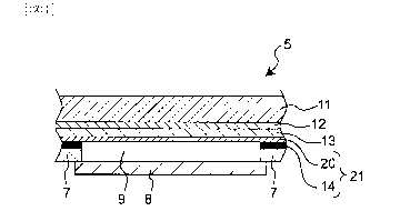
[Fig. 4] Fig. 4 is a schematic view that shows a
cross-sectional structure of the protective plate in
accordance with the present embodiment;
[Fig. 5] Fig. 5 is a schematic view that shows a
modified example of a crc>ss-sectional structure of the
protective plate in accordance with the present embodiment;
[Fig. 6A] Fig. 6A is a view that shows a state of
a polymer dispersion-type liquid crystal film, with no
voltage being applied thereto;
[Fig. 6B] Fig. 6B is a view that shows a state of
the polymer dispersion-type liquid crystal film, with a
voltage being applied thereto; and
[Fig. 7] Fig. 7 is a functional block diagram
showing a portable telephone terminal, in which attention
is focused on the function of the display-protective plate
of the portable telephone terminal of Fig. 1 for making
changes in designing.
Best Mode for Carrying Out the Invention
Referring to the drawings, the following
description will discuss a portable telephone terminal on
which a display-protective plate for an electronic
apparatus in accordance with one embodiment of the present
invention is mounted.
CA 02692353 2009-12-31
12
Fig. 1 is an outside structural view that shows a
portable telephone terminal on which a display-protective
plate for an electronic apparatus in accordance with the
one embodiment of the present invention is mounted, and Fig.
2 is a cross-sectional view that shows an upper-side main
body of the portable telephone terminal of Fig. 1. A
portable telephone terminal 1 is provided with an upper-
side main body 2 and a lower-side main body 3, and the
upper-side main body 2 is allowed to slide relative to the
lower-side main body 3 as indicated by an arrow 50 so that
the open/close states of the lower-side main body 3 can be
switched.
A liquid crystal display 4 is installed on the
upper-side main body 2, and a protective plate 5 is bonded
to the entire surface of a case 7 so as to protect the
liquid crystal display 4. The case 7 of the upper-side
main body 2 is formed into a box shape, and a liquid
crystal display panel 8 is housed therein. The liquid
crystal display panel 8 has its portion exposed from an
opening 9 of the case, which forms the display 4 that is
visually recognizable from the outside. The liquid crystal
display panel 8 is made of a normally black liquid crystal
panel that looks black in a non-display state.
The protective plate 5 is attached to the surface
of the case 7 to cover the entire case so that it protects
-~, ~= ~~~ u 'i nPrPZore, Lne QiULeL Llve {J1dLC ..,, UJCU l UL
CA 02692353 2009-12-31
13
the display 4, and also imparts a designing effect to the
upper-side main body 2. Here, in Fig. 2, there is an air
layer 9 between the surface of the liquid crystal display
panel 8 and the protective plate 5; however, this air layer
is not necessarily required to be formed.
Moreover, operation buttons 6 are provided to the
lower-side main body 3, and in its open state, these are
exposed to the outside to be made operable for inputting
processes. That is, the upper-side main body 2 also
functions as a protective member for the operation buttons
6 on the lower-side main body.
When the upper-side main body 2 is in its closed
state, that is, when the operation buttons 6 on the lower-
side main body are covered, and are not used for inputting
processes, the portable telephone terminal is set to a
stand-by state. Moreover, when the upper-side main body 2
is in its open state, that is, the operation buttons 6 are
exposed and can be used f'or the inputting processes, the
portable telephone terminal 1 is set to a usable state, and
the corresponding state arid the like are displayed on the
display 4. Therefore, the protective plate 5, used for
covering the surface of the upper-side main body 2, is
allowed to have an outside appearance corresponding to the
displayed state of the display 4 that is changed depending
on the state of the portable telephone terminal.
CA 02692353 2009-12-31
14
In the present ernbodiment, the display mode of
the upper-side main body 2 of the portable telephone
terminal can be switched among three display designs shown
in Figs. 3A to 3C. In a mode shown in Fig. 3A, the entire
surface of the upper-side main body 2 is in a decorated
state with an emphasized reflective gloss so that the
display 4, covered with the protective plate 5, is not
visually recognizable. Thi_s state is a state where, since
a polymer dispersion-type liquid crystal film 13, located
beneath a color half mirror layer, which will be described
later, is in a non-transniitting mode, reflection of the
color half mirror layer loc:ated thereon is emphasized. In
a mode shown in Fig. 3B, the entire surface of the upper-
side main body 2 exhibits an outside appearance like a
color half mirror, with the presence of the display 4 being
visually recognized very faintly. This state is a state
where, since the polymer dispersion-type liquid crystal
film 13 located beneath the color half mirror layer is
transparent, a reflection-increasing film layer and a
backing layer, located beneath the film, become more
recognizable from the surface, rather than the reflection
of the color half mirror layer, with its color standing out
on the surface. In a mode shown in Fig. 3C, the entire
surface of the upper-side main body exhibits an outside
appearance like a color half mirror, with the display 4
CA 02692353 2009-12-31
being in its displayed state. This state is a decorated
state where, as described above, the reflection-increasing
film layer and the backing layer, located beneath the color
half mirror layer, are recognizable from the surface, with
5 the display 4 being in the displayed state. The portable
telephone terminal relating to the present embodiment makes
it possible to switch among these states by having the
following structure.
Fig. 4 is a schematic view that shows a cross-
10 sectional structure of the protective plate relating to the
present embodiment. Fig. 5 is a schematic view that shows
a modified example of a cross-sectional structure of the
protective plate relating to the present embodiment. The
protective plate 5 is configured by successively laminating
15 a plate-shaped transparent base member 11, a color half
mirror layer 12, placed on the lower side of the
transparent base member 17., that is made of a metal thin
film subjected to a tint treatment, the polymer dispersion-
type liquid crystal film 13, formed on the lower face of
the color half mirror layer 12, that is one example of a
transparency-switching film capable of switching between
transmitting and non-transmitting modes, a transparent
reflection-increasing film layer 20, formed on the lower
face of the polymer dispersion-type liquid crystal film 13,
that is a composite film formed by alternately laminating
CA 02692353 2009-12-31
16
high refractive-index films and low refractive-index films,
and a backing layer 14 that is formed on a portion of the
display panel 8 except fos- the exposed portion thereof,
with being made in tightly contact, with the lower face of
the reflection-increasing film layer without having an air
layer interposed therebetween.
Here, Fig. 4 shows an example in which the
polymer dispersion-type liquid crystal film 13 with the
half color mirror layer _.2 directly affixed thereto is
attached onto the surface of the transparent base member 11
with a transparent bonding agent (not shown), and Fig. 5
shows an example in which the transparent base member 11, a
half mirror film with a half mirror layer affixed onto the
surface thereof, and an adhesive film formed by applying a
transparent bonding agent to the surface of a polymer
dispersion-type liquid crystal film are mutually bonded one
after another.
The transparent base member 11 is a plate-shaped
member that is superior in transparency and capable of
protecting the display from damage. A desired pattern may
be affixed onto the surface of the transparent base member
11. The transparent base member 11 is made from a
synthetic resin or reinfo:-ced glass or the like. Examples
of the synthetic resin include: general-purpose resins,
such as a polystyrene-based resin, a polyolefin-based resin,
CA 02692353 2009-12-31
17
an ABS resin, an AS resin, an acrylic-based resin, and an
AN resin. Moreover, the examples further include: general
purpose engineering resins, such as a polyphenylene oxide-
polystyrene-based resin, a polycarbonate-based resin, a
polyacetal-based resin, a polycarbonate-modified
polyphenylene ether resin, a polybutylene terephthalate
resin and an ultra-high molecular weight polyethylene resin,
and super engineering resins, such as a polysulfone resin,
a polyphenylene sulfide-based resin, a polyphenylene oxide-
based resin, a polyallylate resin, a polyether imide resin,
a polyimide resin, a liquid crystal polyester resin, and a
polyallyl-based heat resistant resin. Although the
transparent base member 11_ is a plate-shaped member, the
plate-shaped member is not limited to a flat plate as
illustrated, but includes a thin molded product having a
curved face.
Moreover, in a case of using reinforced glass as
the transparent base member 11, although the material is
not particularly limited, rather than generally-used so-
called blue glass, white soda glass (so-called white glass)
that is further superior in mechanical strength and the
like may be preferably used. With respect to the method
for manufacturing reinforced glass (the method for a
reinforcing process), although not particularly limited,
normally a reinforcing method by the use of ion exchange is
CA 02692353 2009-12-31
18
preferably used since a glass plate having a thickness of
about 1 mm is used in most cases. The chemically
reinforced glass, reinforced through ion exchange, is
allowed to exhibit a greater compression stress in
comparison with wind-cooled reinforced glass, as described
earlier.
Although not particularly limited, the thickness
of the transparent base member 11 is preferably set in a
range of from about 0.3 to 1.1 mm, more preferably, from
0.5 to 0.8 mm, from the viewpoint of achieving light weight
while maintaining sufficient strength.
The color half m=_rror layer 12 is arranged on the
surface of the polymer dispersion-type liquid crystal film
13, and bonded to the back surface of the transparent base
member 11 by using a bonding agent or the like. As shown
in Fig. 4, it may be directly arranged on the surface of
the polymer dispersion-type liquid crystal film 13, or as
shown in Fig. 5, a half mirror film 17, formed by affixing
the color half mirror layer 12 to the back face of a
transparent film 16 formed separately from the polymer
dispersion-type liquid crystal film 13, may be arranged so
as to be bonded to the polymer dispersion-type liquid
crystal film 13 with a transparent bonding agent 18. Here,
the transparent film 16 and the color half mirror layer 12
may be switched with each other in their order of
CA 02692353 2009-12-31
19
laminations.
Examples of the transparent film 16 forming the
half mirror film 17 include engineering plastic materials,
such as polycarbonate-based, polyamide-based and polyether
ketone-based plastic materials, and resins, such as acryl-
based, polyethylene terephthalate-based and polybutylene
terephthalate-based resins..
The color half m__rror layer 12 is made of a metal
thin film that is subjected to a tint treatment. The term
"tint" means a transparent color ink that is exemplified as
a pigment ink or a dye ink having an extremely low density.
Specific examples of the tint treatment include a method in
which a metal thin film such as aluminum, chromium, tin or
indium is formed on the su.rface of the polymer dispersion-
type liquid crystal film 13 by means of vapor deposition or
the like, when a pigment having an extremely low density is
applied thereon through a gravure printing method as its
tint treatment. Moreove:_-, a metal thin film layer is
formed on the surface of the transparent film 16, and a
gravure printing process inay be carried out thereon. In
still another tint treatment, a colored transparent resin
film may be used as the transparent film 16. In this case,
the colored transparent resin film having a desired tint to
be applied may be used. For example, a yellow-colored
transparent film 16 may be combined with a metal thin film
CA 02692353 2009-12-31
having silver gloss to provide a surface gloss with a gold
color.
The metal thin film may be formed by using, for
example, a vacuum vapor deposition method, a sputtering
5 method, a CVD method, a roll coater method or the like.
Here, the metal thin film is preferably formed to have such
a film thickness that, although the metal thin film
conceals the display in a light-off state, it allows
displayed information in a light display state to transmit.
10 The metal thin film is preferably formed so as to have a
light transmittance in a range of from 60 to 80%.
The polymer dispersion-type liquid crystal film
13 is a film capable of switching between non-transmitting
and transmitting states depending on the presence and
15 absence of a voltage application, and its degree of
transmittance can be freely changed by changing the voltage
to be applied. As shown in Figs. 6A and 6B, the polymer
dispersion-type liquid crystal film 13 has a structure in
which a transparent polymer film 42 formed by dispersing
20 capsules 40 of nematic liquid crystal 41 therein is
sandwiched between two sheets of films 43, each having a
transparent conductive film affixed thereto.
The polymer dispersion-type liquid crystal film
13, which is used as an adhesive film 19 formed by applying
a transparent bonding agent 18 to the surface of a film
CA 02692353 2009-12-31
21
having the above-mentioned structure, is attached onto the
surface of the half mirror film 17.
As shown in Fig. 6A, in a state with no voltage
applied thereto, since the liquid crystal 41 having rod-
shaped molecules are aligned along the inner wall of each
capsule 40, light L, ma.de incident on the film, is
refracted in the surface and the inside of the capsule 40
by a difference in refrac'_ive inde.xes of the polymer and
the liquid crystal and by birefringence of the liquid
crystal. As a result, the light L is not allowed to
progress straight and is scattered so that the film looks
white.
In contrast, as shown in Fig. 6B, upon
application of a voltaqe, since the liquid crystal
molecules 41 behave so as to be aligned in the direction in
which the voltage is applied, the liquid crystal molecules
41 are aligned perpendicularly to the electrodes. In this
state, the capsules 40 are brought into a state equivalent
to a no-interface state, and the light L, made incident
thereon, is allowed to progress straight without being
scattered. As a result, t:ne film looks transparent.
The reflection-increasing film layer 20 is made
of a transparent reflection-increasing film. More
specifically, this is made of a composite film in which
high refractive-index films and low refractive-index films
CA 02692353 2009-12-31
22
are alternately laminated. This composite film increases
reflection of light having a specific wavelength by
interference of light rays occurring on the interface
between the high refractive-index film and the low
refractive-index film. When the reflection-increasing film
layer 20 is made to have high reflection of 60% or more, it
becomes possible to apply a tint. With respect to the
combination between the high refractive-index film and the
low refractive-index film., for example, a combination
between a Ti02 film and a Si02 film, or the like is
preferably used. Moreover, the composite film is formed
into a structure with three layers to ten layers on demand,
with each layer being set to 100 nm or less, based upon a
tint to be applied. The method for forming the composite
film includes an EB vapor deposition method, a sputtering
method and the like.
The backing layer is preferably formed so as to
be made tightly in contact with the lower face of the
reflection-increasing film layer 20, with no air layer
being interposed therebetween. In the case when an air
layer is interposed, reflection occurs on the interface,
with the result that the backing layer portion tends to
look white.
The backing layer 14 is made of a solid pattern.
In the present embodiment, a black-colored solid pattern is
CA 02692353 2009-12-31
23
adopted so as to match the color of the liquid crystal
display panel 8 in the light-off state. By allowing the
color of the liquid crystal display panel in the light-off
state and the color of the backing layer 14 to match each
other, the border between the portion of the backing layer
14 and the exposed portion of the display 4 can be made
hardly recognizable visually in the light-off state of the
liquid crystal display panel 8.
The polymer dispersion-type liquid crystal film
13 can make different the color of the protective plate 5
that is visually recognized through the half mirror layer
12 by a shutter effect. That is, when the polymer
dispersion-type liquid crystal film 13 is in the non-
transmitting mode, the light that has reached the polymer
dispersion-type liquid crystal film 13 is reflected by the
white polymer dispersion-type liquid crystal film 13 so
that the color half mirror layer 12 on the white background
is viewed. In contrast, in the case when the polymer
dispersion-type liquid crystal film 13 is in the
transmitting mode, since the polymer dispersion-type liquid
crystal film 13 is transparent, the light, made incident
thereon, is allowed to transmit the color half mirror layer
12 and the polymer dispersion-type liquid crystal film 13
so that colored reflected light from the reflection-
increasing film layer 20 with the backing layer-formed is
CA 02692353 2009-12-31
24
visually recognized. By varying the decorative reflection
colors formed by the color half mirror layer 12 and the
reflection-increasing film layer and the backing layer 14,
the colors of the two layers may be mixed to form another
color tone, and consequently, variations of various colors
can be obtained.
That is, the portable telephone terminal 1 on
which the display-protective plate for an electronic
apparatus in accordance with the present embodiment is
mounted is capable of switching between the modes shown in
Figs. 3A, 3B, and 3C in its designing effect given by the
protective plate 5 as explained above, by switching between
the displayed states of the liquid crystal display, as well
as between transmitting and non-transmitting modes of the
polymer dispersion-type liquid crystal film 13.
That is, in a state shown in Fig. 3A, by bringing
the polymer dispersion-type liquid crystal film 13 into the
non-transmitting mode while the liquid crystal display 8 is
off, the color half mirror layer 12 is visually recognized
on the white background so that a mirror state having
reflective gloss, colored by the color half mirror layer 12,
is prepared over the entire portion. In a state shown in
Fig. 3B, by bringing the polymer dispersion-type liquid
crystal film 13 into the transmitting mode while the liquid
crystal display 8 is off, an outside appearance of the half
CA 02692353 2009-12-31
mirror on the background of colors formed by the
reflection-increasing film layer 20 and the backing layer
14 is prepared.
The portable telephone terminal 1 on which the
5 display-protective plate for an electronic apparatus in
accordance with the presen-= embodiment is mounted makes it
possible to distinguish the state of the portable telephone
terminal 1 at a glance, by making the designing effect
given by the protective plate 5 different depending on the
10 state of the portable telephone terminal 1.
Moreover, the display-protective plate for an
electronic apparatus in accordance with the present
embodiment may have a structure in which, in place of the
metal thin film subjected to a tint treatment, the color
15 half mirror layer 12 is made of a reflection-increasing
film that has been tint-treated. That is, in this
structure, the tint-treated reflection-increasing film and
the transparent reflection-increasing film are used for
sandwiching the polymer dispersion-type liquid crystal film
20 13 from the front side and the back side, respectively.
Since no metal material is contained therein, this
structure is desirably used for applications that call for
an electric wave transmitting property in the protective
plate. The structure and the forming method for the above-
2S mentioned reflection-increasing film layer 20 may be
CA 02692353 2009-12-31
26
applied to a reflection-increasing film for use in the
color half mirror layer 12. Moreover, the tint treatment
for the metal thin film may be applied to the tint
treatment for the reflection-increasing film. Here, the
reflection-increasing film for use in the color half mirror
layer 12 is desirably designed to have such a film
thickness that, although it conceals the display in the
light-off state, it allows a screen display in a light
display state to transmit. Moreover, the reflection-
increasing film to be used for the color half mirror layer
12 is preferably formed so as to have a light transmittance
in a range of from 60 to 80%.
Fig. 7 is a functional block diagram showing a
portable telephone terminal, in which attention is focused
on the function of the display-protective plate of the
portable telephone terminal of Fig. 1 for making changes in
designing. This control system 30 includes a control unit
31 for determining the state of the portable telephone
terminal 1 based upon detection signals from various
functional blocks explained below, and managing the entire
control operations, an open/close determining unit 32 used
for determining the open/close state of the upper-side main
body, a display control unit 33 for controlling the
display/non-display state of the liquid crystal display
panel 8, a switch input unit 34 for detecting whether or
CA 02692353 2009-12-31
27
not an input through the operation buttons 6 of the lower-
side main body 3 is given, and a film voltage applying unit
35 for controlling a voltage to be applied to the polymer
dispersion-type liquid crystal film 13. The control unit
31 determines the state of the portable telephone terminal
1 based upon detection signals from the open/close
determining unit 32 and the switch input unit 34, and
controls the conditions of the display control unit 33 and
the film voltage applying unit 35.
As shown in T'ables 1 and 2, the portable
telephone terminal varies the design of the display-
protective plate depending on the states of the portable
telephone terminal. The design of the display-protective
plate is varied depending on the stand-by state, the power-
off state, and the display state. Here, Table 1 shows how
the electronic apparatus looks when both of the hues that
are exhibited by the reflection-increasing film layer and
the half color mirror layer are similar bluish colors, and
Table 2 shows how the electronic apparatus looks when the
hues that are exhibited by the reflection-increasing film
layer and the half color mirror layer are a blue color and
an orange color, which are respectively different.
CA 02692353 2009-12-31
28
[Table 1]
State Power-Off Stand-by Display state
state
Reflection-
increasing Blue Blue Blue
film layer
Metallic
Half mirror color with.
layer faint blue Transmitted Transmitted
color
reflection.
Liquid Clouded Transparent Transparent
crystal film
Display Off Dark or off Light
Screen
Appearance of Faint blue-- Bluish black- display of
panel color mirrcr color mirror bluish black-
color mirror
Example of
Fig. 3A Fig. 3B Fig. 3C
appearance
[Table 2]
State Power-Off Stand-by Display state
state
Reflection-
increasing film Blue Blue Blue
layer
Metalli.c
Half mirror color with
layer faint orange Transmitted Transmitted
color
reflection
Liquid crystal Clouded Transparent Transparent
film
Display Off Dark or off Light
Faint Screen
Appearance of Blue-color display of
panel orange-color mirror blue-color
mirror
mirror
Example of
Fig. 3A Fig. 3B Fig. 3C
appearance
CA 02692353 2009-12-31
29
As shown in Tab:les 1 and 2, in the power-off
state of the power supply, the entire portion shown in Fig.
3A is brought into a state with mirror-like reflection
gloss by the color half mirror layer 12. At this time, the
display is set in the power-off state by the display
control unit 33, and since a clouded un-transmitting mode
is formed with no voltage being applied to the polymer
dispersion-type liquid crystal film 13 so that the display
is concealed, the panel a;ppearance exhibits the color of
the color half mirror layer 12.
In the stand-by state, the entire appearance, as
shown in Fig. 3B, exhibits a mirror mode with a color
exerted by the reflection-__ncreasing film. In the stand-by
state, the power supply of the portable telephone terminal
1 is on, with no input being given through the switch input
unit 34 for a predetermined period of time. In this state,
the polymer dispersion-type liquid crystal film 13 becomes
transparent, with a voltage being applied thereto by the
film voltage applying unit 35, the entire panel exhibits
the mirror color of the reflection-increasing film by the
reflection-increasing film layer 20 and a black-based half
mirror 21 of the backing layer 14. In the case when the
color half mirror layer 12 and the reflection-increasing
film layer 20 have colors of the same type, as shown in
Table 1, a color closer to the color of the reflection-
CA 02692353 2009-12-31
increasing film layer 20 is exhibited. In contrast, in the
case when the color half mirror layer 12 and the
reflection-increasing film layer 20 have colors of
different types, as shown in Table 2, a mixed color thereof
5 is exhibited. Moreover, the liquid crystal display 4 is in
a dark displayed state or in a light-off state, and can be
visually recognized very faintly.
In the displayed state, the display 4 is allowed
to display a mirror color of the reflection-increasing film,
10 as shown in Fig. 3C. The display state is switched upon
detection of the open state of the upper-side main body by
the open/close determining unit 32 or upon detection of a
switch input through the switch input unit 34, in the
stand-by state. In the display state, the polymer
15 dispersion-type liquid crystal film 13 becomes transparent,
with a voltage being applied thereto by the film voltage
applying unit 35, the entire panel exhibits the mirror
color of the reflection-increasing film by the black-based
backing layer 14. Moreover, the liquid crystal display 4
20 is in a light display state, and the liquid crystal display
can be visually recognized on the background of the mirror
color of the reflection-increasing film.
As described above, in the portable telephone
terminal in accordance with the present embodiment, by
25 controlling the display modes of the display and the
CA 02692353 2009-12-31
31
voltage applied to the liquid crystal film, depending on
the state of the portable telephone, the background color
of the color half mirror is made different so that it is
possible to make the designing effect of the protective
plate different.
By properly combining the arbitrary embodiments
of the aforementioned various embodiments, the effects
possessed by the embodimenzs can be produced.
Industrial Applicability
The display-protective plate for an electronic
apparatus in accordance with the present invention makes it
possible to protect a display to be used in many electronic
apparatuses, and also to improve the designing effect of
the electronic apparatus.
Although the present invention has been fully
described in connection with the preferred embodiments
thereof with reference to the accompanying drawings, it is
to be noted that various changes and modifications are
apparent to those skilled in the art. Such changes and
modifications are to be understood as included within the
scope of the present invention as defined by the appended
claims unless they depart therefrom.