Note: Descriptions are shown in the official language in which they were submitted.
CA 02694507 2010-02-23
Method for operation of a converter circuit, and
apparatus for carrying out the method
DESCRIPTION
Technical field
The invention relates to the field of power
electronics. It relates in particular to a method for
operation of a converter circuit, and to an apparatus
for carrying out the method as claimed in the
precharacterizing clause of the independent claims.
Prior art
Nowadays, converter circuits are used in a multiplicity
of applications. One converter circuit, whose voltage
can be scaled particularly easily is specified in the
WO 2007/023064 Al. In this document, the converter
circuit has a first and a second partial converter
system, wherein the partial converter systems are
connected in series to one another via two series-
connected inductances. The junction point between the
two series-connected inductances forms an output
connection for example for an electrical load. Each
partial converter system has at least one two-pole
switching cell, wherein, when there are a plurality of
switching cells in one partial converter system, these
switching cells are connected in series to one another.
Each two-pole switching cell has two series-connected
controllable bidirectional power semiconductor switches
with a controlled unidirectional current flow
direction, and a capacitive energy store which is
connected in parallel with the series circuit formed by
the power semiconductor switches.
A conventional apparatus, as is shown in Figure 1, is
provided for operation of a converter circuit according
CA 02694507 2010-02-23
- 2 -
to WO 2007/023064 Al, which has a first control circuit
for production of a control signal for controlling the
power semiconductor switches in the switching cells of
the first partial converter system, and has a second
control circuit for production of a further control
signal for controlling the power semiconductor switches
in the switching cells of the second partial converter
system.
The converter circuit according to WO 2007/023064 Al is
typically operated such that a pure AC voltage and a
pure alternating current are produced at the output
connection. The capacitive energy stores for the
switching cells are designed such that the voltage
ripple on the capacitive energy stores remains within a
predetermined fluctuation range for a given maximum
current at the output connection and for this current
being at a given frequency. If a lower frequency is
desired than that on which the design was based, then
the voltage ripple rises. If the intention is to
produce a direct current or an alternating current with
a direct-current component at the output connection,
then the voltage ripple rises to virtually infinity.
The capacitive energy stores in this case would either
have to be fed externally or would have to be selected
to be infinitely large in order to avoid being
completely discharged or indefinitely overcharged
during operation with direct current or a direct-
current component at the output connection.
A method for operation of a converter circuit according
to WO 2007/023064 Al, which allows the capacitive
energy stores to be designed independently of the
desired current at the output connection, that is to
say independently of the frequency of this current, is
not known at the moment.
CA 02694507 2010-02-23
- 3 -
Description of the invention
One object of the invention is therefore to specify a
method for operation of a converter circuit, by means
of which the capacitive energy stores in the converter
circuit can be designed to be independent of the
desired current at the output connection of the
converter circuit, that is to say to be independent of
its frequency. A further object of the invention is to
specify an apparatus by means of which the method
according to the invention can be carried out in a
particularly simple manner.
These objects are achieved by the features of claim 1
and claim 10, respectively. Advantageous developments
of the invention are specified in the dependent claims.
A converter circuit has a first and a second partial
converter system, wherein the partial converter systems
are connected in series to one another via two series-
connected inductances. The junction point of the two
series-connected inductances forms an output
connection. Each partial converter system comprises at
least one two-pole switching cell, and each switching
cell has two series-connected controllable
bidirectional power semiconductor switches with a
controlled unidirectional current flow direction and a
capacitive energy store which is connected in parallel
with the series circuited formed by the power
semiconductor switches. The number of switching cells
in the first partial converter system preferably
corresponds to the number of switching cells in the
second partial converter system. According to the
method, the power semiconductor switches in the
switching cells of the first partial converter system
are controlled by means of a control signal, and the
power semiconductor switches in the switching cells of
the second partial converter system are controlled by
CA 02694507 2010-02-23
- 4 -
means of a further control signal. According to the
invention, the control signal is now formed from a
voltage oscillation signal across the inductances and a
switching function for the power semiconductor switches
in the switching cells of the first partial converter
system, and the further control signal is formed from
the voltage oscillation signal across the inductances
and a switching function for the power semiconductor
switches in the switching cells of the second partial
converter system, wherein the switching functions are
formed by means of a voltage oscillation signal with
respect to the voltage at the output connection and a
selectable reference signal, in particular at the same
time. By means of the applied oscillations, that is to
say by means of the voltage oscillation signal across
the inductances for the production of the control
signal and the further control signal, and by means of
the voltage oscillation signal with respect to the
voltage at the output connection for production of the
switching functions, it is advantageously possible to
ensure that the voltage ripple on the capacitive energy
stores can be reduced significantly when a desired
current is flowing at the output connection of the
converter circuit, which means that the capacitive
energy stores may be designed only with respect to the
voltage ripple, which has now been reduced, and are
therefore independent of the desired output current.
The apparatus according to the invention for carrying
out the method for operation of the converter circuit
has a first control circuit, which is used for
production of the control signal and is connected to
the power semiconductor switches in the switching cells
of the first partial converter system. Furthermore, the
apparatus has a second control circuit, which is used
to produce the further control signal and is connected
to the power semiconductor switches in the switching
cells of the second partial converter system. According
CA 02694507 2010-02-23
- 5 -
to the invention, in order to form the control signal,
the first control circuit is now supplied with the
voltage oscillation signal across the inductances and
the switching function for the power semiconductor
switches in the switching cells of the first partial
converter system. In order to form the further control
signal, the second control circuit is supplied with the
voltage oscillation signal across the inductances and
the switching function for the power semiconductor
switches in the switching cells of the second partial
converter system. Furthermore, a first calculation unit
is provided in order to calculate the switching
functions from a voltage oscillation signal with
respect to the voltage at the output connection and a
selectable reference signal. The apparatus according to
the invention for carrying out the method for operation
of the converter circuit can therefore be produced very
easily and at low cost, since the circuit complexity
can be kept extremely low and, furthermore, only a
small number of components are required for
construction. The method according to the invention can
therefore be carried out particularly easily by means
of this apparatus.
These and further objects, advantages and features of
the present invention will become obvious from the
following detailed description of preferred embodiments
of the invention and in conjunction with the drawing.
Brief description of the drawings
In the figures:
Figure 1 shows one embodiment of an apparatus for
carrying out a method for operation of a
converter circuit according to the prior
art,
CA 02694507 2010-02-23
- 6 -
Figure 2 shows one embodiment of an apparatus
according to the invention for carrying
out the method according to the
invention for operation of a converter
circuit,
Figure 3 shows a time profile of a current at the
output connection of the converter
circuit,
Figure 4 shows a time profile of a voltage at the
output connection of the converter
circuit, and
Figure 5 shows a time profile of the current
through the first partial converter
system and the current through the
second partial converter system.
The reference symbols used in the drawing, and their
meanings, are listed in summarized form in the list of
reference symbols. In principle, the same parts are
provided with the same reference symbols in the
figures. The described embodiments represent examples
of the subject matter according to the invention, and
have no restrictive effect.
Approaches to implementation of the invention
As already mentioned initially, Figure 1 shows one
embodiment of an apparatus for carrying out a method
for operation of a converter circuit according to the
prior art. Figure 2 shows one embodiment of an
apparatus according to the invention for carrying out
the method according to the invention for operation of
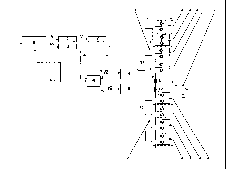
a converter circuit. The converter circuit shown in
CA 02694507 2010-02-23
- 7 -
Figure 2 has a first and a second partial converter
system 1, 2, wherein the partial converter systems 1, 2
are connected in series to one another via two series-
connected inductances L1, L2. The junction point
between the two series-connected inductances L1, L2
forms an output connection A. Each partial converter
system 1, 2 in general has at least one two-pole
switching cell 3. One partial converter system 1, 2 has
a plurality of switching cells 3, these switching cells
3 are connected in series to one another, as shown in
Figure 2. Each switching cell 3 has two series-
connected controllable bidirectional power
semiconductor switches with a controlled unidirectional
current flow direction and a capacitive energy store
which is connected in parallel with the series circuit
formed by the power semiconductor switches. The
controllable power semiconductor switches are, in
particular, in the form of gate turn-off thyristors
(GTO) or integrated thyristors with a commutated
control electrode (IGCT - Integrated Gate Commutated
Thyristors), each with a diode connected back-to-back
in parallel. However, it is also feasible for a
controllable power semiconductor switch to be, for
example, in the form of a power MOSFET with a diode
additionally connected back-to-back in parallel with
it, or in the form of a bipolar transistor with an
insulated gate electrode (IGBT) and a diode
additionally connected back-to-back in parallel with
it. The number of switching cells 3 in the first
partial converter system 1 preferably corresponds to
the number of switching cells 3 in the second partial
converter system 2.
According to the method, the power semiconductor
switches in the switching cells 3 of the first partial
converter system 1 are controlled by means of a control
signal Si, and the power semiconductor switches in the
switching cells 3 of the second partial converter
CA 02694507 2010-02-23
- 8 -
system 2 are controlled by means of a further control
signal S2. The control signal Si for the switching
cells 3 in the first partial converter system 1 and the
control signal S2 for the switching cells 3 in the
second partial converter system 2 are offset in time
with respect to one another for each switching cell 3,
as a result of which each switching cell 3 can
advantageously be controlled with a time offset.
According to the invention, the control signal Si is
now formed from a voltage oscillation signal VL across
the inductances Li, L2 and a switching function a, for
the power semiconductor switches in the switching
cells 3 of the first partial converter system 1, in
particular from the sum of the two variables, and the
further control signal S2 is formed from the voltage
oscillation signal VL across the inductances L1, L2 and
a switching functions a2 for the power semiconductor
switches in the switching cells 3 of the second partial
converter system 2, in particular from the sum of the
two variables, wherein the switching functions al, a2
are formed by means of a voltage oscillation signal VA
with respect to the voltage Vu at the output connection
A and a selectable reference signal Vref in particular
at the same time. A reference voltage signal with
respect to the voltage Vu at the output connection A is
preferably selected as the reference signal Vref and is
formed, for example, by regulation of the actual value
of the current iu at the output connection A at a
nominal value.
As a result of the applied oscillations, that is to say
by means of the voltage oscillation signal VL across the
inductances L1, L2 for production of the control signal
Si and the further control signal S2, and by means of
the voltage oscillation signal VA with respect to the
voltage Vu at the output connection A in order to
produce the switching functions al, a2, it is
advantageously possible to ensure that the voltage
CA 02694507 2010-02-23
- 9 -
ripple on the capacitive energy stores can be
significantly reduced for a desired current iu at the
output connection A of the converter circuit, which
means that the capacitive energy store need be designed
only for the voltage ripple which has now been reduced,
and therefore independently of the desired output
current iu.
According to the invention, the switching function al
for the power semiconductor switches in the switching
cells 3 of the first partial converter system 1 is
formed from the voltage oscillation signal VA with
respect to the voltage Vu of the output connection A and
the selectable reference signal Vref using the following
formula:
al = %(1-Vref-VA) [1]
Furthermore, a switching function a2 for the power
semiconductor switches in the switching cells 3 of the
second partial converter system 2 is formed from the
voltage oscillation signal VA with respect to the
voltage Vu at the output connection A and the selectable
reference signal Vref using the following formula:
a2 = %z(1+Vref+VA) [2]
According to the invention, the voltage oscillation
signal VL across the inductances L1, L2 is formed from a
current oscillation signal Vi of the partial converter
system 1, 2, as illustrated by the following formula:
VL = Vi. (j() (L1 + L2) ) [3]
The current oscillation signal Vi of the partial
converter system 1, 2 is preferably in turn formed from
a current oscillation signal amplitude value Ah, in
particular by multiplication of the current oscillation
CA 02694507 2010-02-23
- 10 -
signal amplitude value Ah by an oscillation at a freely
variable frequency m and a phase shift cp, as
illustrated by the following formula:
Vi = Ah 'COS ((Ot+(P) [41
The current oscillation signal amplitude value Ah is in
general formed from the current actual value iu at the
output connection A, in particular from the direct-
current component io of the current iu at the output
connection A which current actual value iu is, for
example, measured, and the reference signal Vref. The
following relationship as shown in formula [5.1] is
used to form the current oscillation signal amplitude
value Ah:
3' lo=Mh2+Ah=Mh=COS (Atp) - (l+Vref) = (1-Vref) =10=0 [5.11
and, for example, using formula [5.2]
Ah = Mh [5.2]
where AT in general indicates the phase difference
between the applied oscillations and the voltage V. at
the output connection A. It should be noted that the
ratio of Ah to Mh in formula [5.2] has been selected
only by way of example, that is to say the ratio of Ah
to Mh can in general be selected freely. Formula [5.1]
therefore may be solved only for the product
oscillation signal amplitude vale Ah in order to
determine the current oscillation signal amplitude
value Ah.
Furthermore, the voltage oscillation signal VA with
respect to the voltage Vu at the output connection A is
in general formed from a voltage oscillation signal
amplitude value Mh, preferably by multiplication of the
voltage oscillation signal amplitude value Mh by an
CA 02694507 2010-02-23
- 11 -
oscillation at freely variable frequency m and a phase
shift cp, as illustrated by the following formula:
VA = Mh=cos ((Ot+cp) [6]
In general, the voltage oscillation signal amplitude
value Mh is formed from the current actual value iu at
the output connection A and the reference signal Vref,
in which case it is advantageously possible to make use
of the formulae [5.1] and [5.2] , and the formula [5.1]
need be solved for the voltage oscillation signal
amplitude value Mh only to determine the voltage
oscillation signal amplitude value Mh.
The current oscillation signal Vi of the partial
converter systems 1, 2, the voltage oscillation signal
VL across the inductances L1, L2 and the voltage
oscillation signal VA with respect to the voltage Vu of
the output connection A are preferably at the same
frequency w. Furthermore, the current oscillation
signal Vi of the partial converter systems 1, 2, the
voltage oscillation signal VL across the inductances L1,
L2 and the voltage oscillation signal VA with respect to
the voltage Vu at the output connection A advantageously
have the same phase shift cp, wherein they need not
necessarily have the same phase shift T.
On the basis of the method according to the invention,
it is now advantageously possible to produce a current
iu with a direct-current component and with an
alternating current component at the frequency w, which
is based on the applied oscillations mentioned above,
at the output connection A, wherein only the applied
oscillations influence the voltage ripple on the
capacitive energy stores of the switching cells 3, and
the voltage ripple can therefore be kept low. The
capacitive energy stores can therefore now
advantageously be designed only with respect to this
CA 02694507 2010-02-23
- 12 -
low voltage ripple, that is to say independently of the
desired output current i,,. The current iu at the output
connection A accordingly becomes:
i (t) = 10 + COS(wt + (4)) [7]
where io represents said direct-current component and
represents the amplitude of said alternating-current
component. For illustrative purposes, Figure 3 shows a
time profile of a current iõ at the output connection of
the converter circuit. Furthermore, Figure 4 shows a
time profile of a voltage Vu of the output connection A
of the converter circuit. Finally, Figure 5 shows a
time profile of the current it through the first partial
converter system 1 and of the current i2 through the
second partial converter system 2, wherein both
currents i1, i2 likewise have a direct-current component
and an alternating-current component at the frequency
w, caused by the abovementioned applied oscillations.
For the sake of completeness, it should be mentioned
that the currents in the capacitive energy stores do
not have any direct-current component and likewise have
no alternating-current components at the frequency w,
or else at twice the frequency w of the abovementioned
applied oscillations.
In a polyphase system, for example in a three-phase
system with three converter circuits, the applied
oscillations, if they are selected to have the same
phase shifts, appear as a common-mode voltage on a
polyphase load which is connected to the phase
terminations A. No additional current oscillations are
produced. This method is used, for example, in the
event of overmodulation. In contrast to overmodulation,
the frequency and phase angle of the common-mode
voltage are in this case undefined. The output current
io, which is then a polyphase output current, is a pure
CA 02694507 2010-02-23
13 -
direct current, that is to say it has no alternating-
current components.
If the current iu of the output connection A is intended
to have a desired alternating-current component 'u
=cos (wut+(pu) at the frequency wu and with a desired
phase shift (pu, when the formula [5.1] is modified as
follows:
2 + Ah = Mh cos(4(p) - (1 + V,af) = (1- V,.r) = ~ = cos(wut + (p,,) = 0 [8)
1 ~ = cos(w,,t + c)u) = Mh2
where formula [5.2] can once again be used to determine
the current oscillation signal amplitude value Ah, and
the current oscillation signal amplitude value Ah and
the voltage oscillation signal amplitude value Mh can be
determined as already described above, from formula [8]
and formula [5.2]. The current iu of the output
connection A then, in the desired manner, becomes:
iõ(t) _ %, = cos(o t + (põ) + , = cos(wt + (p) [9]
where U is an assumed current amplitude value.
The apparatus according to the invention as shown in
Figure 1 has a first control circuit 4 which is used to
produce the control signal Sl and is connected to the
power semiconductor switches in the switching cells 3
of the first partial converter system 1. Furthermore, a
second control circuit 5 is provided, which is used to
produce the further control signal S2 and is connected
to the power semiconductor switches in the switching
cells 3 of the second partial converter system 2.
According to the invention, in order to form the
control signal Si, the first control circuit 4 is
supplied with the sum of the voltage oscillation signal
VL across the inductances Ll, L2 and the switching
function al for the power semiconductor switches in the
switching cells 3 of the first partial converter
CA 02694507 2010-02-23
- 14 -
system 1. In order to form the further control signal
S2, the second control circuit 5 is supplied with the
sum of the voltage oscillation signal VL across the
inductances L1, L2 and the switching function a2 for
the power semiconductor switches in the switching cells
3 of the second partial converter system 2. By way of
example, a look-up table is in each case used to form
the control signal Si and the further control signal
S2, in the first and second control circuits 4, 5, in
which the switching function al is permanently
associated with corresponding control signals Sl, and
in which the switching function a2 is permanently
associated with corresponding further control signals
S2 or, for example, a modulator in each case, which is
based on a method for pulse-width modulation.
Furthermore, a first calculation unit 6 is provided in
order to form the switching functions al, a2 by
calculation using formulae [1] and [2] from the voltage
oscillation signal VA with respect to the voltage Vu at
the output connection A and a selectable reference
signal Vref
As shown in Figure 2, a second calculation unit 10 is
provided in order to form the voltage oscillation
signal VL across the inductances Ll, L2 from a current
oscillation signal Vi of the partial converter
systems 1, 2, wherein the second calculation unit 10
forms the voltage oscillation signal VL across the
inductances Li, L2 by calculation by means of the
formula [3].
Furthermore, a third calculation unit (7) is provided
in order to form the current oscillation signal Vi of
the partial converter systems 1, 2 from a current
oscillation signal amplitude value Ah, and forms the
current oscillation signal Vi of the partial converter
systems 1, 2 by calculation using the formula [4].
CA 02694507 2010-02-23
- 15 -
Furthermore, a fourth calculation unit 9 is provided in
order to form the current oscillation signal amplitude
value Ah from the current actual value iu at the output
connection A and the reference signal Vref, wherein the
fourth calculation unit 9 forms the current oscillation
signal amplitude value Ah by calculation using the
formlae [5.1] and [5.21, or using the formulae [8]
and [ 5 . 2 ] .
A fifth calculation unit 8 which is provided is used to
form the voltage oscillation signal VA with respect to
the voltage Vu at the output connection A from a voltage
oscillation signal amplitude value Mh, wherein the fifth
calculation unit 8 forms the voltage oscillation signal
VA with respect to the voltage Vu at the output
connection A by calculation using formula [6].
The already mentioned fourth calculation unit 9 is
likewise used to form the voltage oscillation signal
amplitude value Mh from the current actual value iu at
the output connection A and the reference signal Vref,
wherein the fourth calculation unit 9 forms the voltage
oscillation amplitude value Mh by calculation using the
formulae [5.1] and [5.2], or using the formulae [8] and
[5.2].
Overall, it has been possible to show that the
apparatus according to the invention, in particular as
shown in Figure 2, for carrying out the method
according to the invention for operation of the
converter circuit can be produced very easily and at
low cost, since the circuit complexity is extremely low
and, furthermore, only a small number of components are
required for construction. This apparatus therefore
allows the method according to the invention to be
carried out particularly easily.
CA 02694507 2010-02-23
- 16 -
List of reference symbols
1 First partial converter system
2 Second partial converter system
3 Switching cell
4 First control circuit
5 Second control circuit
6 First calculation unit
7 Third calculation unit
8 Fifth calculation unit
9 Fourth calculation unit
10 Second calculation unit