Note: Descriptions are shown in the official language in which they were submitted.
CA 02695263 2012-10-22
27957-55
4
ELECTRIC POWER CONVERSION APPARATUS FOR VEHICLE
FIELD OF THE INVENTION
The present invention relates to an electric power conversion
apparatus, which is connected to an electric motor used as an actuator for an
in-
vehicle device such as an electric power steering system for a vehicle.
BACKGROUND OF THE INVENTION
In a conventional electric power conversion apparatus, mechanical
relays are used to shut off electric connection between motor phase terminals
of a
three-phase electric motor and output terminals of an inverter circuit. If
such a
mechanical relay is used, reliability of its operation is lowered by foreign
matters and
the like, which are often jammed. The following patent document therefore
proposes
to use a power MOS-type field effect transistor in place of such a mechanical
relay.
[Patent document] JP 2006-21645A
According to this proposal, the transistors are connected between a
three-phase electric motor and an inverter circuit so that electrical
connection and
disconnection therebetween is controlled by a voltage applied to the gate of
the
transistor.
If a current required by the electric motor is increased, the amount of
heat generated by the transistor tends to excessively increase in a period, in
which
the transistor is turned on to electrically connect the inverter circuit and
the electric
motor. If the heat generated by the transistor excessively increases, the
reliability of
the transistor will be lowered.
SUMMARY OF THE INVENTION
It is therefore an object of some embodiments of the present invention
to provide an electric power conversion apparatus, which is capable of
maintaining
- 1 -
CA 02695263 2013-12-27
=
27957-55
reliability of a transistor connected between an electric power conversion
circuit and
an electric motor used as an actuator in a vehicle.
According to an aspect of the present invention, an electric power
conversion apparatus is provided for a vehicle having an electric motor as an
electric
actuator of an in-vehicle device. The apparatus comprises an electric power
conversion circuit and a power transistor. The transistor has a gate terminal,
a
source terminal and a drain terminal, and connects an output terminal of the
electric
power conversion circuit and a motor terminal of the electric motor through
the source
terminal and the drain terminal. The power transistor has the source terminal
positioned between the gate terminal and the drain terminal.
According to one aspect of the present invention, there is provided an
electric power conversion apparatus for a vehicle having an electric motor as
an
electric actuator of an in-vehicle device, the apparatus comprising: an
electric power
conversion circuit; and a power transistor having a gate terminal, a source
terminal
and a drain terminal and connecting an output terminal of the electric power
conversion circuit and a motor terminal of the electric motor through the
source
terminal and the drain terminal, the power transistor including a gate, a
drain and a
source of a semiconductor chip and having the source terminal positioned
between
the gate terminal and the drain terminal, wherein: the gate terminal, the
drain terminal
and the source terminal are connected to the gate, the drain and the source of
the
semiconductor chip, respectively; the drain terminal of the power transistor
is
connected to the motor terminal of the electric motor; the semiconductor chip
is a
vertical-type, which has the source and the gate on one surface thereof and
the drain
on another surface opposite to the one surface; and the drain terminal has one
part,
which is on the another surface and in a rectangular shape larger than the
another
surface in area size, and another part, which extends from one of four corners
of the
rectangular shape in parallel to the gate terminal and the source terminal;
and the
source terminal is shorter than the another part of the drain terminal.
- 2 -
CA 02695263 2013-12-27
27957-55
According to another aspect of the present invention, there is provided
an electric power conversion apparatus for a vehicle having an electric motor
as an
electric actuator of an in-vehicle device, the apparatus comprising: an
electric power
conversion circuit; and a plurality of power transistors connecting a
plurality of outputs
of the electric power conversion circuit and a plurality of motor terminals of
the
electric motor, respectively, each power transistor having a gate, a source
and a
drain on a semiconductor chip and connecting one output terminal of the
electric
power conversion circuit and one motor terminal of the electric motor through
the
source and the drain, each power transistor having a source terminal
positioned
between a gate terminal and a drain terminal, wherein: the gate terminal and
the
drain terminal are provided adjacently to the source terminal in the each
power
transistor; the drain terminal of each power transistor is connected to a
corresponding
one of the motor terminals; the each power transistor is formed of a vertical-
type
semiconductor, which has the source and the gate on one surface of the
semiconductor chip and the drain on another surface of the semiconductor chip
opposite to the one surface; and the drain terminal has one part, which is on
the
another surface and in a rectangular shape larger than the another surface in
area
size, and another part, which extends from one of four corners of the
rectangular
shape in parallel to the gate terminal and the source terminal; and the source
terminal
is shorter than the another part of the drain terminal.
BRIEF DESCRIPTION OF THE DRAWINGS
The above and other objects, features and advantages of the present
invention will become more apparent from the following detailed description
made
with reference to the accompanying drawings. In the drawings:
FIG. 1 is a circuit diagram showing an electric power conversion
apparatus according to a first embodiment of the present invention;
FIGS. 2A to 2C are schematic views showing configuration and
arrangement of a semiconductor relay used in the first embodiment;
- 2a -
CA 02695263 2013-12-27
=
27957-55
FIG. 3 is a circuit diagram showing an electric power conversion
apparatus according to a second embodiment of the present invention; and
FIGS. 4A and 4B are circuit diagrams partly showing semiconductor
relays according to modification of the first and second embodiments.
DETAILED DESCRIPTION OF THE PREFERRED EMBODIMENT
An electric power conversion apparatus for a vehicle according to the
present invention will be described in detail below with reference to
embodiments, in
which the apparatus is connected to an electric motor used in an electric
power
steering system, for example.
(First Embodiment)
Referring first to FIG. 1, a steering system for a vehicle provided as an
in-vehicle device includes a steering wheel 10, an input shaft 12, a
- 2b -
CA 02695263 2010-03-04
transmission 20, drive wheels 22 and the like. The steering wheel 10 is
operable by a driver to change direction of travel of the vehicle. The input
shaft 12 is rotatable in accordance with rotation operation of the steering
wheel 10. The input shaft 12 is mechanically coupled with a main gear 14 to
rotate together about the same rotation axis.
The main gear 14 is engaged with an assist gear 16. The assist gear
16 is mechanically coupled with an output shaft 18a of an electric motor 18 to
rotate together about the same rotation axis.
The input shaft 12 is also mechanically coupled to the transmission 20
at its end, which is opposite to the steering wheel 10. The transmission 20 is
provided to transfer the rotation of the input shaft 12 to the drive wheels by
changing a ratio of the rotation. Thus, the steering wheel 10 is mechanically
coupled to the drive wheels 22.
With the electric motor 18, the assist gear 16 and the like, the steering
system operates as an electric power steering system. The electric motor 18
is provided as an electric actuator of the electric power steering system, so
that it assists the steering operation of the driver in manually operating the
steering wheel 10 to change the steering angle of the vehicle.
The electric motor 18 is a three-phase electric motor. The electric
motor 18 is supplied with electric power of a battery 30 through an inverter
circuit IV. The inverter circuit IV has a first series connection of switching
elements Sup, Sun, a second series connection of switching elements Svp, Svn
and a third series connection of switching elements Swp, Swn between the
battery 30 and the ground. The junctions in the first, second and third series
connections are connected to motor phase terminals of the windings of
U-phase, V-phase and W-phase of the electric motor 18, respectively.
N-channel power MOS field effect transistors Tru, Trv, Trw are used as the
switching elements Sup, Sun, Svp, Svn, Swp, Swn and include respective body
diodes Dup, Dun, Dvp, Dvn, Dwo, Dwn.
It becomes impossible to generate assist torque by the electric motor
18 in operating the power steering system, if a switching element of the
inverter circuit IV has a short-circuit failure, for example. Even in this
instance,
the short-circuited part or the diode remains as a current supply path to the
-3-
CA 02695263 2010-03-04
electric motor 18. The electric motor 18 operates as an electric power
generator. As a result, torque is applied in reverse to the manual operation
of
the steering wheel 10 by the driver. It will thus become difficult for the
driver
to operate the steering wheel manually when the electric power steering
system fails to short-circuit.
To avoid such difficulty, semiconductor relays Tru, Trv, Trw are provided
between output terminals of the three phases of the inverter circuit IV and
motor terminals of the three phases of the electric motor 18. Each of the
semiconductor relays Tru, Trv, Trw is also a N-channle power MOS field effect
transistor. Each of the transistor is formed with a body diode (Bdu, Bdv,
Bdw),
which is connected to be forward-biased from the source terminal to the drain
terminal. That is, the anode and the cathode of each body diode Bdu, Bdv,
Bdw are connected to the source and the drain of each semiconductor relay
Tru, Trv, Trw. In the following description, the semiconductor relays Tru,
Trv,
Trw and the diodes Bdu, Bdv, Bdw are generally referred to as a semiconductor
relay Tr,and a diode Tr.
The source terminal of the semiconductor relay Tr is connected to the
output terminal of the inverter circuit IV.
The drain terminal of the
semiconductor relay Tr is connected to the motor terminal of the electric
motor
18. All of the diodes Bdu, Bdv, Bdw are connected to be forward-biased from
the inverter circuit IV to the electric motor 18.
Thus, when the semiconductor relay Tr is turned off, the inverter circuit
IV and the electric motor 18 are electrically shut off or disconnected from
each
other surely. The semiconductor relay Tr is formed with the diode Bd.
Therefore, even when the semiconductor relay Tr is turned off, a current is
allowed to flow between the output terminal of the inverter circuit IV and the
motor terminal of the electric motor 18 through the diode Bd. According to
the Kirchhoff's law, the sum of the three-phase currents of the electric motor
18 is zero. It is therefore necessary that, for a current to flow to the
electric
motor 18, there should be one phase, through which a current flows into the
electric motor 18, and another phase, through which a current flows out from
the electric motor 18. That is, two electric paths are required so that one
electric path allows the current to flow from the inverter circuit IV to the
-4-
CA 02695263 2010-03-04
electric motor 18 and the other electric path allows the current to flow from
the electric motor 18 to the inverter circuit Iv. Therefore, by arranging all
the
diodes Bdu, Bdv, Bdw in the same current flow (bias) direction as described
above, it is surely prevented that the currents flow in the electric motor 18
when all the semiconductor relays Tru, Trv, Trw are turned off. That is, the
inverter circuit Iv and the electric motor 18 are electrically disconnected
from
each other surely.
The drain terminal of the semiconductor relay Tr is connected to the
motor terminal of the electric motor 18, because the withstand voltage
between the gate terminal and the drain terminal of the semiconductor relay Tr
is higher than that between the gate terminal and the source terminal of the
same. Since the current changes when the switching elements of the inverter
circuit Iv are turned on and off, inductance component of the electric motor
18
generates surge in the currents. This surge is also applied to the
semiconductor relay Tr. The semiconductor relay Tr therefore should be
sufficiently resistive to withstand such surge. It is effective to utilize the
withstand voltage between the gate terminal and the drain terminal of the
semiconductor relay Tr as a countermeasure to the surge of the electric motor
18 so that the required withstand voltage of the semiconductor relay Tr may be
lowered as much as possible. For this reason, the drain terminal of the
semiconductor relay Tr is connected to the terminal of the electric motor 18.
The semiconductor relay Tr is controlled to be in the turned-on
condition while the manual operation of the steering wheel 10 should be
assisted. It is very likely that the heat generated by the semiconductor relay
Tr increases, because the current flowing in the electric motor 18 is
comparatively large (for example, several tens to a hundred and several tens
of
amperes, assumedly more than 90 amperes). The semiconductor relay Tr is
configured and arranged as shown in FIGS. 2A to 2C.
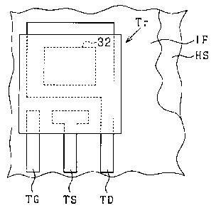
As shown in FIG. 2A, which is a top plan view, the transistor Tr has the
drain terminal TD on its rear face side. The drain terminal TD is positioned
to
face a heat sink HS through an insulation film layer IF, which is provided as
a
heat insulation member. The heat sink HS is a heat radiation member and
may be formed of aluminum or the like.
-5-
CA 02695263 2010-03-04
=
A semiconductor chip 32 of the semiconductor relay Tr is a vertical-type.
Specifically, the semiconductor chip 32 is formed with a source region and a
gate on its front (main) face side. The semiconductor chip 32 is formed with
a drain area on the opposite side (rear face side) thereof. As shown in FIG.
2B, which is a bottom plan view, the drain terminal TD occupies most part of
the rear face side of the transistor Tr. The drain terminal TD is shown as
being exposed. According to this configuration, the drain area of the
semiconductor chip 32 can be sized large to have high heat radiation
performance. With the increased area of the drain terminal TD, the heat
generated in the drain area can be radiated sufficiently. Since the drain
terminal TD faces the heat sink HS, the heat radiation performance of the
drain
terminal TD is further enhanced.
The source region of the semiconductor chip 32, on the other hand,
tends to be sized smaller than the drain region, although the same amount of
current flows in both areas. Since the front face side of the semiconductor
chip 32 is formed with not only the source region but also a part for contact
with the gate, an area of contact between an electrical conductor (material of
high thermal conductivity), which contacts the source region of the
semiconductor chip 32, and the source region is limited.
Therefore, the semiconductor relay Tr is configured to have the source
terminal TS between the gate terminal TG and the drain terminal TD. That is,
the source terminal TS is positioned between the gate terminal TG and the
drain terminal TD with respect to terminal parts, which extend in parallel one
another on the same plane, among the gate terminal TG, the drain terminal TD
and the source terminal TS. The distance between the semiconductor chip 32
and the source terminal TS can be shortened in comparison with a case, in
which the drain terminal TD is positioned between the gate terminal TG and
the source terminal TS. It is shown in FIG. 2C that the length of a part of a
bonding wire 34, which electrically connects the source region and the source
terminal TS of the semiconductor chip 32, between the source region and the
source terminal TS is shorter than that of a part of a bonding wire 36, which
electrically connects the gate and the gate terminal TG, between the gate and
the gate terminal TG. The part of the bonding wire 34 between the source
-6-
CA 02695263 2010-03-04
region and the source terminal TS does not contact a high thermal conductivity
material and has a small surface area. Thus this part is inferior to the
source
terminal TS and the like with respect to heat radiation performance. It is
preferred therefore to shorten the length of such a part as much as possible
to
enhance heat radiation performance in the source region. For this reason, the
source terminal TS is positioned between the gate terminal TG and the drain
terminal TD in the semiconductor relay Tr.
As described above, since the heat radiation performance of the drain
terminal is high, the heat generated near the drain terminal TD can be
radiated
effectively by the heat radiation performance of the drain terminal TD. As a
result, in the electric power steering system shown in FIG. 1, the heat
generated at the electric motor 18 side can be radiated to the heat sink HS
through the drain terminal TD.
The first embodiment has the following features.
(1) The semiconductor relay Tr has the source terminal TS between the
gate terminal TG and the drain terminal TD. As a result, the heat generated
in the source region can be radiated speedily to the source terminal TS. Thus,
the temperature of the semiconductor relay Tr can be suppressed from rising
and hence the reliability of the semiconductor relay Tr can be suppressed from
being lowered.
(2) The drain region of the semiconductor chip 32 forming the
semiconductor relay Tr is arranged to face the heat sink HS through the
insulation film layer IF. As a result, the heat generated in the drain region
can
be speedily radiated to the heat sink HS.
(3) Each of the output terminals of the inverter circuit IV is connected to
the corresponding one of the terminals of the electric motor 18 through one
relay Tr. Further, the drain terminal TD of the semiconductor relay Tr is
connected to the electric motor 18. As a result, the electric connection and
disconnection between the inverter circuit IV and the electric motor 18 can be
performed appropriately by controlling the voltage applied to the gate of the
semiconductor relay Tr. In addition, the capability of withstanding surge at
the electric motor 18 side can be increased and the heat generated at the
electric motor 18 side can be appropriately radiated.
-7-
CA 02695263 2010-03-04
(Second Embodiment)
An electric power conversion apparatus according to the second
embodiment is shown in FIG. 3, in which the same or similar parts are
designated by the same reference numerals as in the first embodiment.
In the second embodiment, the drains of the semiconductor relays Tru,
Trv, Trw are connected to the output terminals of the inverter circuit IV. As
a
result, even if the electric path between the semiconductor relay Tr and the
electric motor 18 is short-circuited to the ground, it is prevented that a
short-circuit current flows from the battery 30 to the ground through the
diode
Bd of the semiconductor relay Tr. Since the drain of the semiconductor relay
Tr has higher heat radiation performance, heat radiation at the inverter
circuit
IV side can be promoted by arranging the drain at the inverter circuit IV
side.
The second embodiment has the following features in addition to the
features (1) and (2) of the first embodiment.
(4) Each of the output terminals of the inverter circuit IV is connected to
the corresponding one of the terminals of the electric motor 18 is connected
through one semiconductor relay Tr, and the drain terminal TD of the
semiconductor relay Tr is connected to the inverter circuit IV. As a result,
the
electrical connection and disconnection between the inverter circuit IV and
the
electric motor 18 can be appropriately performed by controlling the voltage
applied to the gate of the semiconductor relay Tr. Further, even if the
electric
motor 18 side is short-circuited to the ground, a short-circuit current is
prevented from flowing through the diode Bd of the semiconductor relay Tr.
Still further, the heat generated at the inverter circuit IV side can be
appropriately radiated to the heat sink HS.
(Modification)
The first and the second embodiments may be modified as follows.
The transistor provided as the semiconductor relay Tr in each electric
path between the inverter circuit IV and the electric motor 18 is not limited
to
one in number. For example, as shown in FIGS. 4A and 4B, a pair of
transistors Tr1 and Tr2 may be provided as the semiconductor relay Tr in each
electric path or phase of the electric motor 18. In these examples, the
transistors Tr1 and Tr2 in each electric path are connected such that the
-8-
CA 02695263 2010-03-04
anodes of respective body diodes Bd1 and Bd2 of the transistors Tr1 and Tr2
are connected to each other as shown in FIG. 4A or the cathodes of the same
are connected to each other as shown in FIG. 4B. According to this
arrangement, electrical connection between the inverter circuit IV and the
electric motor 18 can be surely shut off. In the example of FIG. 4A, the drain
of one of the transistors Tr1 and Tr2, specifically transistor Tr2, is
connected to
the electric motor 18 side and the drain of the other transistor Tr1 is
connected
to the inverter circuit IV side. As a result, the heat radiation performance
of
the drain terminals of the pair of transistors Tr1 and Tr2 can be
advantageously
utilized to radiate heat generated by the electric motor 18 and the inverter
circuit IV.
The semiconductor relay Tr, which is provided as a switch for
electrically connecting and disconnecting the electric motor 18 and the
inverter
circuit IV, is not limited to the N-channel MOS field effect transistor but
may be
a P-MOS field effect transistor.
The electric motor 18 is not limited to the three-phase brushless DC
motor but may be a DC motor with brushes. In this case, the electric power
conversion circuit IV may be configured as a conventional bridge circuit in
place of the inverter circuit IV shown in FIGS. 1 and 3. In connecting the
motor terminals of the electric motor 18 and the output terminals of the
electric power conversion circuit IV through the power transistors, the
advantages (3) of the first embodiment and (4) of the second embodiment can
be attained by connecting the same terminals (anode or cathode) of the body
diodes to the motor terminals of the electric motor 18.
The electric power steering system is not limited to the disclosed type
but may be a different type, which is equipped with a variable gear system
(VGS). In this different type of power steering system, the electric power
conversion circuit may be provided, since such a system also needs a function
of interrupting electrical connection between an electric power conversion
circuit and an electric motor.
-9-