Note: Descriptions are shown in the official language in which they were submitted.
CA 02695403 2015-07-30
MEASURING SYSTEM FOR CONTACTLESS DECOUPLING OF A SIGNAL
RUNNING ON A SIGNAL WAVEGUIDE
Description
The present invention relates to a contactless
measuring system comprising at least one test probe forming
part of a coupling structure for contactless decoupling of a
signal running on a signal waveguide, wherein the signal
waveguide is configured as a conductor track and as part of
an electric circuit on a circuit board of the electrical
circuit. The invention also relates to a calibration
substrate for a contactless measuring system comprising at
least one test probe forming part of a coupling structure
for contactless decoupling of a signal running on a signal
waveguide, wherein at least one calibration element, in
particular a short-circuit standard, an open circuit
standard, a resistance standard or a conductor standard is
provided on the calibration substrate, wherein the at least
one calibration element is electrically connected to at
least one signal waveguide, in particular a microstrip
transmission line or a coplanar waveguide.
The determination of scattering parameters of
electrical components embedded within a complex circuit by
means of a contactless vector network analysis is known, for
example from T. Zelder, H. Eul, "Contactless network
analysis with improved dynamic range using diversity
calibration", Proceedings of the 36th European Microwave
Conference, Manchester, UK, pages 478 to 481, September 2006
or T. Zelder, H. Rabe, H. Eul, "Contactless electromagnetic
measuring system using
1
CA 02695403 2010-02-02
conventional calibration algorithms to determine
scattering parameters", Advances in Radio Science -
Kleinheubacher Berichte 2006, vol. 5, 2007. Compared with
conventional contact-bound network analysis methods, the
internal directional couplers of a network analyser are
replaced with contactless near field measuring probes
which are directly connected to the vectorial measuring
points of the analyser. The measuring probes are
positioned over the signal lines of the object being
measured. The probes can act inductively and/or
capacitively on the electromagnetic field of the planar
conductor. In order to measure the scattering parameters,
conventional calibration methods are used, such as are
used for contact-bound network analysis.
In contactless vector network analysis, for each
measuring port of an unknown test object (DUT - Device
Under Test), at least one measuring probe, for example, a
conductor loop or two capacitive probes are needed. It is
known from, for example, F. De Groote, J. Verspecht, C.
Tsironis, D. Barataud and J.-P. Teyssier, "An improved
coupling method for time domain load-pull measurements",
European Microwave Conference, vol. 1, pages 4 ff.,
October 2005, to use contactless conductor loops made
from coaxial semi-rigid lines. By contrast, it is known
from T. Zelder, H. Eul, "Contactless network analysis
with improved dynamic range using diversity calibration",
Proceedings of the 36th European Microwave Conference,
Manchester, UK, pages 478 to 481, September 2006 or T.
Zelder, H. Rabe, H. Eul, "Contactless electromagnetic
measuring system using conventional calibration
algorithms to determine scattering parameters", Advances
in Radio Science - Kleinheubacher Berichte 2006, vol. 5,
2
CA 02695403 2015-07-30
2007, to use exclusively capacitive probes in contactless
measuring systems. From T. Zelder, I. Rolfes, H. Eul,
"Contactless vector network analysis using diversity
calibration with capacitive and inductive coupled
probes", Advances in Radio Science - Kleinheubacher
Berichte 2006, vol. 5, 2007 and J. Stenarson, K. Yhland,
C. Wingqvist, "An in-circuit noncontacting measurement
method for S-parameters and power in planar circuits",
IEEE Transactions on Microwave Theory and Techniques,
vol. 49, No. 12, pages 2567 to 2572, December 2001,
measuring systems are known which are realised with a
combination of capacitive and inductive probes.
Although contactless vector network analysis has the
potential of characterising components contactlessly, to
date no contactless scattering parameter measurement of
HF and microwave components embedded within a circuit has
been performed. If measurements are to be made within a
circuit, the positions of the contactless probes must be
changed during and after the calibration. However, this
implies a high level of complexity in order to reproduce
the test probe positions during measurement of the
calibration standard and of the test object, since the
smallest deviations in the probe positioning lead to
significant measuring errors.
It is an object of the invention to provide a
contactless measuring system of the aforementioned type
such that expensive and complex positioning of coupling
probes can be dispensed with.
This aim is achieved according to the invention with
a contactless measuring system of the aforementioned type
and with a calibration substrate of the aforementioned
type.
3
CA 02695403 2015-07-30
,
With a contactless measuring system of the
aforementioned type, it is provided according to the
invention that at least one contact structure is
configured and arranged on the circuit board such that
said contact structure is galvanically separated from the
signal waveguide, forms part of the coupling structure,
is arranged completely within the near field of the
signal waveguide and comprises at least one contact point
which can be electrically contacted by a contact of a
test probe.
This has the advantage that the contact structure
and thus the whole coupling structure has a precisely
defined geometrical arrangement relative to the signal
waveguide, wherein manual positioning of the coupling
structure can be dispensed with. Reproducible coupling
between the signal waveguide and the coupling structure
can be easily achieved.
Suitably, the contact structure is configured as a
conductor track on the circuit board.
Particularly good signal coupling can be achieved in
that the contact structure is configured so that said
contact structure can be contacted by a test probe in
impedance-controlled manner.
At least one contact structure is configured, for
example, as a coupling waveguide with an inner conductor
and an outer conductor or as at least one contact point
or contact surface for a contact of a test probe.
4
CA 02695403 2010-02-02
Suitably, the contact structure and/or the signal
waveguide is configured as printed conductor tracks on
the circuit board.
For example, the circuit board is configured as a
printed circuit board (PCB) or a wafer.
Optimal directional damping or a port with wide-band
insulation is achieved in that the contact structure is
configured as a waveguide, wherein the ratio of the
inductive to the capacitive coupling factor is equal to
the product of the wave impedances of the individual
waveguides of the contact structure.
In an exemplary embodiment, the coupling structure
has at least one, in particular two, contact structures
per measuring port.
In a preferred embodiment, the circuit board is a
multi-layer board with a plurality of substrate layers,
wherein the signal waveguide is configured on a first
substrate layer of the multi-layer board and at least one
contact structure is configured on the first or at least
one other substrate layer of the multi-layer board.
As an example, at least two of the contact
structures are arranged on different substrate layers of
=
the multi-layer board.
In a particularly preferable embodiment, the at
least one contact structure has contact points which are
configured and arranged such that contacting with on-
wafer or PCB test probes results in an impedance-
controlled interface.
For rapid and simple calibration of the contactless
measuring system, also arranged on the circuit board is
at least one calibration element, which is connected to
;
at least one signal waveguide on which at least one
=
5
=
CA 02695403 2010-02-02
contact structure is arranged such that the arrangement
of the contact structure on the signal waveguide of a
calibration element corresponds to the arrangement of the
contact structures on the signal waveguides of the
electrical circuit.
At least one calibration element is connected to a
number of signal waveguides which corresponds to the
number of measuring ports of the contactless measuring
system.
In order to provide the calibration elements and the
electrical circuit with identical coupling conditions and
optimum calibration, at least one contact structure on
the signal waveguides of the calibration elements, said
contact structure being assigned to a measuring port of
the contactless measuring system, is configured
identically to the at least one contact structure on the
signal waveguides of the electrical circuit, said contact
structure being assigned to said measuring port of the
contactless measuring system.
With a calibration substrate of the aforementioned
type it is provided, according to the invention, that the
calibration substrate is configured as a circuit board,
on which at least one contact structure is configured and
arranged such that this contact structure is galvanically
separated from the signal waveguide, forms part of the
coupling structure, is arranged completely within the
near field of the signal waveguide and has at least one
contact point which is electrically contactable with a
contact of a test probe.
This brings the advantage that the contact structure
and thus the overall coupling structure has a precisely
defined geometrical arrangement to the signal waveguide,
6
CA 02695403 2010-02-02
wherein manual positioning of the coupling structure can
be dispensed with. Reproducible coupling between the
signal waveguide and the coupling structure is achieved
by simple means.
The contactless measuring system is preferably
configured as described above, wherein it is particularly
preferable that at least one contact structure on the
signal waveguides of the calibration elements, said
contact structure being assigned to a measuring port of
the contactless measuring system, is configured
identically to the at least one contact structure on the
signal waveguides of the electrical circuit, said contact
structure being assigned to said measuring port of the
contactless measuring system.
At least one calibration element is connected to a
number of signal waveguides which corresponds to the
number of measuring ports of the contactless measuring
system.
Suitably, on the circuit board of the calibration
substrate, at least one electrical circuit is configured
with at least one signal waveguide on which at least one
contact structure is arranged such that the arrangement
of the contact structure on the signal waveguide
corresponds to the arrangement of the contact structures
on the signal waveguides of a calibration element.
In a preferred embodiment, at least one contact
structure on the signal waveguides of the calibration
elements, said contact structure being assigned to a
measuring port of the contactless measuring system, is
configured identically to the at least one contact
structure on the calibration substrate on the signal
waveguides of the electrical circuit, said contact
7
CA 02695403 2010-02-02
structure being assigned to said measuring port of the
contactless measuring system.
The invention will now be described in greater
detail making reference to the drawings, in which:
Fig. 1 shows a schematic block circuit diagram of a
preferred embodiment of a contactless measuring system
according to the invention with a vector network
analyser,
Fig. 2 shows a first preferred embodiment of a
contact structure for the contactless measuring system
according to the invention,
Fig. 3 shows a second preferred embodiment of a
contact structure for the contactless measuring system
according to the invention,
Fig. 4 shows a first preferred embodiment of a
calibration substrate according to the invention for the
contactless measuring system according to the invention
in plan view,
Fig. 5 shows an exemplary alternative embodiment of
a contact structure for the contactless measuring system
according to the invention,
Fig. 6 shows a further exemplary alternative
embodiment of a contact structure for the contactless
measuring system according to the invention,
Fig. 7 shows a further exemplary alternative
embodiment of a contact structure for the contactless
measuring system according to the invention,
=
Fig. 8 shows a further exemplary alternative
embodiment of a contact structure for the contactless
measuring system according to the invention,
8
CA 02695403 2010-02-02
Fig. 9 shows a further exemplary alternative
embodiment of a contact structure for the contactless
measuring system according to the invention,
Fig. 10 shows a further exemplary alternative
embodiment of a contact structure for the contactless
measuring system according to the invention,
Fig. 11 shows a further exemplary alternative
embodiment of a contact structure for the contactless
measuring system according to the invention,
Fig. 12 shows a further exemplary alternative
embodiment of a contact structure for the contactless
measuring system according to the invention,
Fig. 13 shows a further exemplary alternative
embodiment of a contact structure for the contactless
measuring system according to the invention,
Fig. 14 shows a second preferred embodiment of a
calibration substrate according to the invention for the
contactless measuring system according to the invention
in plan view, and
Fig. 15 shows a third preferred embodiment of a
calibration substrate according to the invention for the
contactless measuring system according to the invention
in plan view.
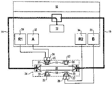
The preferred embodiment of a contactless measuring
system according to the invention shown in Fig. 1
comprises a vector network analyser 10 having a signal
source 12, signal lines 14 and 16 and a contact structure
=
with four coupling waveguides 18, each of which has an
inner conductor 20 and an outer conductor 22. The
coupling waveguides 18 are configured as printed
conductor tracks on a printed circuit board 24. Also
arranged on this printed circuit board 24 is a signal
9
CA 02695403 2014-11-12
=
waveguide 26 configured as a printed conductor track. The
signal waveguide 26 is part of an electronic circuit (not
shown in detail) provided on the printed circuit board 24 with
corresponding electronic components.
The coupling waveguides 18 together with a test probe 28
form a coupling structure for the contactless measuring system
in order to decouple contactlessly an electromagnetic wave
running along the signal waveguide 26. The test probes 28 each
create an electrical contact with a coupling waveguide 18 on
one side, and with the measuring ports 30, 32, 34, 36 of the
vector network analyser 10 on the other side.
The coupling waveguides 18 can be shaped almost
arbitrarily. It is particularly advantageous for the coupling
waveguides 18 to be configured in impedance-controlled manner,
i.e. the characteristic wave impedance values of the
arrangement are known and are optimised for low reflection.
The advantage of an impedance-controlled contact structure
lies therein that optimum directional damping and a port which
is insulated over a broad bandwidth can be achieved.
Two examples of an impedance-controlled coupling waveguide
18 of this type are shown in Figs. 2 and 3. The coupling
waveguide 18 shown in Fig. 2 comprises a U-shaped inner
conductor 20 and an outer conductor 22. The outer conductor 22
can be variously configured. Firstly, the outer conductor 22
can be closed, i.e. the outer conductor arms 38 and 40 close
at the coordinate z = 0, as indicated in Fig. 2 with dashed
lines and secondly, the ends of the outer conductor arms 38, 40
can be separated along z. For example, the arms 38, 40 then
end at the positions +z1 and -z1 or, as shown in Fig. 2, at
CA 02695403 2010-02-02
the positions +z2 and -z2. Through the arrangement of the
outer conductor 22 relative to the inner conductor 20,
the coupling waveguide 18 corresponds to a bent coplanar
waveguide. Different variants of this coupling waveguide
18 are possible. A variant without corners is shown in
Fig. 3. By way of example here, the outer conductor arms
38 and 40 are joined to one another at the position z =
0.
A further advantage of the contact structure
according to the invention is that no through contacts to
earth (rear-sided base metalizing of the circuit board
24) are necessary. However, the possibility of connecting
the outer conductors 22 of the coupling waveguides 18 to
earth with through contacts is not ruled out.
For decoupling energy from the signal waveguide 26
of a test object (DUT - Device Under Test) at least one
contact structure or coupling waveguide 18 is brought
into the near field of the respective signal waveguide
26. The coupling waveguide 18 can be situated on the same
substrate as the respective signal waveguide 26, or in
the case of a multi-layer board, on another substrate.
The contact structure with the coupling waveguides 18 is
then connected, for example, to a commercial symmetrical
on-wafer or PCB test probe. The reference sign 42 in
Figs. 2 and 3 denotes the contact positions of the
contacts of test probes with the contact structure or the
respective coupling waveguide 18. In order to
characterise an N-port test object, at least N coupling
waveguides 18 situated within the near field of the N
signal waveguides 26 are needed. Fig. 1 shows the example
of a 2-port test object (in this case, a simple conductor
= DUT) with four coupling waveguides 18.
11
=
CA 02695403 2010-02-02
The geometry of the coupling waveguides 18 and of
the test probes 28 both influence the coupling factor of
the arrangement. The test probes 28 are connected to
(vectorial) receivers of, for example, a conventional
network analyser, as shown in Fig. 1.
The procedure for measuring test objects embedded
within planar circuits with the aid of at least one
impedance-controlled contact structure or at least one
non-impedance-controlled contact structure within planar
circuits will now be described.
The method is essentially based on the method of
contactless vector network analysis. The disadvantage of
contactless vector network analysis is that the use of
the method for achieving accurate measured values is very
heavily dependent on the positioning accuracy of the
contactless test probes. According to the invention, it
is also provided that printed contact structures are used
in combination with conventional test probes, rather than
a complex automatic positioning system in combination
with completely contactless probes. All the signal lines
of the test objects and of the calibration elements which
are necessary for system error calibration, must be
provided with at least one coupling waveguide 18 (contact
structure).
An example of a practical implementation of a
calibration substrate with embedded test objects (DUT3,
DUT4) making use of contact structures with printed
coupling waveguides 18 is shown in Fig. 4. For 2-port
calibration, the contact structure comprises two coupling
waveguides 18 for each signal waveguide 26, said coupling
waveguides being configured, for example, according to
the embodiment of Fig. 2. For N-port calibration, a
12
CA 02695403 2010-02-02
contact structure with at least N coupling waveguides 18
per signal waveguide 26 is necessary. When using a
diversity calibration method, it is also useful to
utilise a contact structure with more than N coupling
waveguides 18 per signal waveguide 26.
Due to the small dimensions of the coupling
waveguides 18, for example, on-wafer or PCB test probes
can be reproducibly positioned on the identical coupling
waveguides 18 of the individual calibration elements
(LINE1, LINE2, LINE3, LINE4, OPEN, SHORT). Once the
system has been calibrated, the scattering parameters of,
for example, embedded components can be determined.
However, the signal lines of the components must have the
same properties (geometry, wave impedance, etc.) as those
of the calibration elements. In addition, the same
contact structure must be present on the planar circuit
at every signal waveguide 26 of the embedded test object
(DUT) as used for the calibration.
The method therefore involves the placement of a
contact structure, for example, in the form of a coupling
waveguide 18 within the near field of the signal
waveguide 26 of the calibration and test objects on a
circuit board 24. The coupling waveguides 18 are arranged
and configured on the circuit board 24 such that they
barely disrupt the function of a circuit and also can be
connected to, for example, conventional on-wafer or PCB
test probes.
Figs. 5 to 13 illustrate various exemplary
embodiments of contact structures 44. The contact
structures 44 can have very particular forms. In
principle, any desirable form can be used. In order to
create a reproducible coupling between the signal
13
CA 02695403 2010-02-02
waveguide 26 and the coupling waveguide 18 or the signal
waveguide 26 and the test probe 28 or the signal
waveguide 26 and the coupling waveguide 18 and the test
probe 28, the contact structure 44, if said contact
structure comprises a material surface, either has holes
in which the test probe is positioned, or has a marked
geometry on which the test probe is positioned.
Alternatively, the contact structure 44 can also be
configured as a notch in the substrate.
Fig. 14 shows a second preferred embodiment of a
calibration substrate according to the invention which is
configured on a circuit board 46. Parts with the same
function are identified with the same reference numbers
as in Figs. 1 and 4, so that reference is made to the
description relating to Figs. 1 and 4 above for their
elucidation. A plurality of calibration elements 48 is
arranged on the calibration substrate and each
calibration element 48 is connected to one, two or three
signal waveguides 26. As distinct from the first
embodiment according to Fig. 4, no coupling waveguides
are provided on the signal waveguides 26, but rather
contact structures 44 as shown in Figs. 5 to 13. Signals
are optionally fed to the signal waveguide 26 at suitable
contact sites 50. This calibration substrate comprises
different 1-port, 2-port and 3-port calibration standards
48 and different contact structures 44.
Fig. 15 shows a third preferred embodiment of a
calibration standard according to the invention, which is
configured on a circuit board 46. Parts with the same
function are identified with the same reference signs as
in Figs. 1, 4 and 14, so that reference is made to the
description relating to Figs. 1, 4 and 14 above for their
14
CA 02695403 2014-11-12
elucidation. In this embodiment, an electronic circuit 52 is
also provided with components 54 (DUTs) to be tested on the
circuit board 46 of the calibration substrate. Conversely, it
can also be said that calibration elements 48 are also
arranged on the circuit board 46 with the electronic circuit
52. The contact structure 44 for a particular measuring port
on the signal waveguides 26 of the calibration elements are
configured identically to the contact structure 44 for this
measuring port on the signal waveguides 26 of the electronic
circuit 52.
For the correct measurement of the scattering parameters
of an N-port test object, the measuring system must be
calibrated. Depending on the calibration, M different N-port
calibration standards (calibration elements 48), which are
known or only partially known, are needed. For calibration
using M calibration standards, the geometry and the position
of the contact structure and of the signal waveguide 26 must
be identical for each measuring port, although it can be
different between the N measuring ports.
If, for example, the scattering parameters of a 2-port
object are to be measured, then for an LLR calibration, three
2-port calibration standards are needed. These can be, for
example, two lines of different length and two short-
circuits, wherein the short-circuits each represent a 1-port
object, but together correspond to a 2-port object. The three
2-port standards can comprise two different supply lines
(signal waveguides 26) per port. The contact structures 44
can also be different on each supply line (each signal
waveguide) in terms of position and geometry. However, the
signal waveguides 26 and the contact structure 44 must be
CA 02695403 2010-02-02
identical at the respective ports 1 of the calibration
standard and the DUTs 48. Also, at the port 2 of the
calibration standard, the signal waveguides 26 and the
contact structure 44 must match one another, although
they can differ from those at the port 1.
16