Note: Descriptions are shown in the official language in which they were submitted.
CA 02696110 2010-02-10
WO 2009/029548 PCT/US2008/074120
GROWTH OF ORDERED CRYSTALLINE ORGANIC FILMS
CROSS REFERENCE TO PROVISIONAL APPLICATION
[0001] This application claims the benefit of U.S. provisional application No.
60/957,902
filed August 24, 2007, the disclosure of which is incorporated herein by
reference.
[0002] This invention was made with U.S. Government support under Contract No.
FA9550-07-1-0364 awarded by the Air Force Office of Scientific Research. The
government
has certain rights in this invention.
[0003] The present invention generally relates to organic photosensitive films
for use in
electronic devices, to processes for manufacturing such films, and to devices
using such
films.
[0004] Optoelectronic devices rely on the optical and electronic properties of
materials to
either produce or detect electromagnetic radiation electronically or to
generate electricity
from ambient electromagnetic radiation.
[0005] Photosensitive optoelectronic devices convert electromagnetic radiation
into
electricity. Solar cells, also called photovoltaic (PV) devices, are a type of
photosensitive
optoelectronic device that is specifically used to generate electrical power.
PV devices, which
may generate electrical energy from light sources other than sunlight, can be
used to drive
power consuming loads to provide, for example, lighting, heating, or to power
electronic
circuitry or devices such as calculators, radios, computers or remote
monitoring or
communications equipment. These power generation applications also often
involve the
charging of batteries or other energy storage devices so that operation may
continue when
direct illumination from the sun or other light sources is not available, or
to balance the
power output of the PV device with a specific application's requirements. As
used herein the
term "resistive load" refers to any power consuming or storing circuit,
device, equipment or
system.
[0006] Another type of photosensitive optoelectronic device is a
photoconductor cell. In
this function, signal detection circuitry monitors the resistance of the
device to detect changes
due to the absorption of light.
[0007] Another type of photosensitive optoelectronic device is a
photodetector. In
operation a photodetector is used in conjunction with a current detecting
circuit which
measures the current generated when the photodetector is exposed to
electromagnetic
radiation and may have an applied bias voltage. A detecting circuit as
described herein is
1
SUBSTITUTE SHEET (RULE 26)
CA 02696110 2010-02-10
WO 2009/029548 PCT/US2008/074120
capable of providing a bias voltage to a photodetector and measuring the
electronic response
of the photodetector to electromagnetic radiation.
[0008] These three classes of photosensitive optoelectronic devices may be
characterized
according to whether a rectifying junction as defined below is present and
also according to
whether the device is operated with an external applied voltage, also known as
a bias or bias
voltage. As used herein, the term "rectifying" denotes, inter alia, that an
interface has an
asymmetric conduction characteristic, i.e., the interface supports electronic
charge transport
preferably in one direction. A photoconductor cell does not have a rectifying
junction and is
normally operated with a bias. A PV device has at least one rectifying
junction and is
operated with no bias. A photodetector has at least one rectifying junction
and is usually but
not always operated with a bias. As a general rule, a photovoltaic cell
provides power to a
circuit, device or equipment, but does not provide a signal or current to
control detection
circuitry, or the output of information from the detection circuitry. In
contrast, a
photodetector or photoconductor provides a signal or current to control
detection circuitry, or
the output of information from the detection circuitry but does not provide
power to the
circuitry, device or equipment.
[0009] Traditionally, photosensitive optoelectronic devices have been
constructed of a
number of inorganic semiconductors, e.g., crystalline, polycrystalline and
amorphous silicon,
gallium arsenide, cadmium telluride and others. Herein the term
"semiconductor" denotes
materials which can conduct electricity when charge carriers are induced by
thermal or
electromagnetic excitation. The term "photoconductive" generally relates to
the process in
which electromagnetic radiant energy is absorbed and thereby converted to
excitation energy
of electric charge carriers so that the carriers can conduct, i.e., transport,
electric charge in a
material. The terms "photoconductor" and "photoconductive material" are used
herein to
refer to semiconductor materials which are chosen for their property of
absorbing
electromagnetic radiation to generate electric charge carriers.
[0010] PV devices may be optimized for maximum electrical power generation
under
standard illumination conditions (i.e., Standard Test Conditions which are
1000 W/rri ,
AM1.5 spectral illumination), for the maximum product of photocurrent times
photovoltage.
The power conversion efficiency of such a cell under standard illumination
conditions
depends on the following three parameters: (1) the current under zero bias,
i.e., the short-
circuit current Isc, (2) the photovoltage under open circuit conditions, i.e.,
the open circuit
voltage Voc, and (3) the fill factor, ff.
2
CA 02696110 2010-02-10
WO 2009/029548 PCT/US2008/074120
[0011] PV devices produce a photo-generated current when they are connected
across a
load and are irradiated by light. When irradiated under infinite load, a PV
device generates
its maximum possible voltage, V open-circuit, or Voc. When irradiated with its
electrical
contacts shorted, a PV device generates its maximum possible current, I short-
circuit, or Isc=
When actually used to generate power, a PV device is connected to a finite
resistive load and
the power output is given by the product of the current and voltage, I x V.
The maximum
total power generated by a PV device is inherently incapable of exceeding the
product, Isc x
Voc. When the load value is optimized for maximum power extraction, the
current and
voltage have the values, ImaR and VmaR, respectively.
[0012] A figure of merit for PV devices is the fill factor, ff, defined as:
ff=( ImaR VmaR )/( Isc
x Voc ) (1) where ff is always less than 1, as Isc and Voc are never obtained
simultaneously
in actual use. Nonetheless, as ff approaches 1, the device has less series or
internal resistance
and thus delivers a greater percentage of the product of Isc and Voc to the
load under optimal
conditions. Where P,n, is the power incident on a device, the power efficiency
of the device,
ilP, may be calculated by: ilP =ff x ( Isc x Voc)/ Pin,=
[0013] PV devices may be characterized by the efficiency with which they can
convert
incident solar power to useful electric power. Devices utilizing crystalline
or amorphous
silicon dominate commercial applications, and some have achieved efficiencies
of 23% or
greater. However, efficient crystalline-based devices, especially of large
surface area, are
difficult and expensive to produce due to the problems inherent in producing
large crystals
without significant efficiency-degrading defects. On the other hand, high
efficiency
amorphous silicon devices still suffer from problems with stability. Present
commercially
available amorphous silicon cells have stabilized efficiencies between 4 and
8%. More recent
efforts have focused on the use of organic photovoltaic cells to achieve
acceptable
photovoltaic conversion efficiencies with economical production costs.
[0014] Organic PV cells have many potential advantages when compared to
traditional
silicon-based devices. Organic PV cells are lightweight, economical in
materials use, and can
be deposited on low cost substrates, such as flexible plastic foils.
[0015] When electromagnetic radiation of an appropriate energy is incident
upon an
organic semiconductor material, a photon can be absorbed to produce an excited
molecular
state. In organic photoconductive materials, the generated molecular state is
generally
believed to be an "exciton," i.e., an electron-hole pair in a bound state
which is transported as
a quasi-particle. An exciton can have an appreciable life-time before geminate
recombination
3
CA 02696110 2010-02-10
WO 2009/029548 PCT/US2008/074120
("quenching"), which refers to the original electron and hole recombining with
each other (as
opposed to recombination with holes or electrons from other pairs). To produce
a
photocurrent, the electron-hole forming the exciton are typically separated at
a rectifying
junction.
[0016] In the case of photosensitive devices, the rectifying junction is
referred to as a
photovoltaic heterojunction. Types of organic photovoltaic heterojunctions
include a donor-
acceptor heterojunction formed at an interface of a donor material and an
acceptor material,
and a Schottky-barrier heterojunction formed at the interface of a
photoconductive material
and a metal.
[0017] FIG. 1 is an energy-level diagram illustrating an example donor-
acceptor
heterojunction. In the context of organic materials, the terms "donor" and
"acceptor" refer to
the relative positions of the Highest Occupied Molecular Orbital ("HOMO") and
Lowest
Unoccupied Molecular Orbital ("LUMO") energy levels of two contacting but
different
organic materials. If the LUMO energy level of one material in contact with
another is lower,
then that material is an acceptor. Otherwise it is a donor. It is
energetically favorable, in the
absence of an external bias, for electrons at a donor-acceptor junction to
move into the
acceptor material.
[0018] After absorption of a photon 6 in the donor 152 or the acceptor 154
creates an
exciton 8, the exciton 8 disassociates at the rectifying interface. The donor
152 transports the
hole (open circle) and the acceptor 154 transports the electron (dark circle).
[0019] A significant property in organic semiconductors is carrier mobility.
Mobility
measures the ease with which a charge carrier can move through a conducting
material in
response to an electric field. In the context of organic photosensitive
devices, a material that
conducts preferentially by electrons due to a high electron mobility may be
referred to as an
electron transport material. A material that conducts preferentially by holes
due to a high
hole mobility may be referred to as a hole transport material. A layer that
conducts
preferentially by electrons, due to mobility and / or position in the device,
may be referred to
as an electron transport layer ("ETL"). A layer that conducts preferentially
by holes, due to
mobility and / or position in the device, may be referred to as a hole
transport layer ("HTL").
Preferably, but not necessarily, an acceptor material is an electron transport
material and a
donor material is a hole transport material.
4
CA 02696110 2010-02-10
WO 2009/029548 PCT/US2008/074120
[0020] How to pair two organic photoconductive materials to serve as a donor
and an
acceptor in a photovoltaic heterojunction based upon carrier mobilities and
relative HOMO
and LUMO levels is well known in the art, and is not addressed here.
[0021] For additional background explanation and description of the state of
the art for
organic photosensitive devices, including their general construction,
characteristics,
materials, and features, U.S. Patent No. 6,657,378 to Forrest et al., U.S.
Patent No. 6,580,027
to Forrest et al., and U.S. Patent No. 6,352,777 to Bulovic et al. are
incorporated herein by
reference.
[0022] Despite the many advantages of organic PV devices, they typically have
relatively
low external quantum efficiency, on the order of 1% or less. This is, in part,
thought to be
due to the second order nature of the intrinsic photoconductive process. That
is, carrier
generation requires exciton generation, diffusion and ionization or
collection. There is an
efficiency il associated with each of these processes. Subscripts may be used
as follows: P
for power efficiency, EQE for external quantum efficiency, A for photon
absorption, ED for
exciton diffusion, CC for charge collection, and IQE for internal quantum
efficiency. Using
this notation, '1Ip - '1IEQg = '1IA x '1IgD x '1lcc, and '1IEQg = '1IA x
'1I1Qg.
[0023] The progress in increasing the power conversion efficiency (rlP) of
organic
photovoltaic (PV) cells over the last decade is chiefly attributed to the
introduction of the
donor-acceptor (DA) heterojunction which functions as a dissociation site for
strongly bound
photogenerated excitons. Typically, in bilayer DA PV cells with a total
thickness, L, on the
order of the optical absorption length, LA, the absorption efficiency is = 1-
exp(-L/LA) >
50%, if optical interference effects are ignored, and IIA Z 100%. However
since the exciton
diffusion length (LD) in highly disordered organic materials is typically an
order of magnitude
smaller than LA, a large fraction of the photogenerated excitons remains
unused for
photocurrent generation (FIG. 2a), limiting IIEQE, and hence ilP, for this
type of cell. The
exciton diffusion bottleneck has been partially removed through the
introduction of bulk
heterojunctions (FIG. 2b). In a bulk heterojunction, the DA interface is
highly folded and
interdigitated such that photogenerated excitons always find a DA interface
within a distance
LD of their generation site. Currently, state-of-the-art bulk heterojunction
polymer PV cells
have power conversion efficiencies exceeding 5%. A polymer bulk heterojunction
is
typically fabricated by spin-coating a mixture of soluble versions of the
donor and acceptor
materials. During spin-coating and solvent evaporation, the donor and acceptor
materials
phase separate, creating an intricate network. However, this type of cell has
a disadvantage
CA 02696110 2010-02-10
WO 2009/029548 PCT/US2008/074120
in that the diffusion length (LD) of an exciton is typically much less (LD -
50 A) than the
optical absorption length (-500 A), requiring a trade off between using a
thick, and therefore
resistive, cell with multiple or highly folded interfaces, or a thin cell with
a low optical
absorption efficiency. The high series resistance of these bulk heterojunction
amorphous
organic blends limits the active layer thickness, leading to reduced light
absorption, while
exhibiting low fill factor and hence low solar energy conversion efficiency.
[0024] However, the absorption efficiency of bulk heterojunctions are
spatially limited. In
general, the absorption characteristics of a heterojunction are maximized by
selecting donor
materials and acceptor materials with different absorption spectra. If an
incident photon has a
wavelength near an absorption peak of the first material but not the second
material, and the
incident photon transits through the bulk heterojunction predominantly via the
second
material (e.g., passing down the length of a "finger" of the second material),
there is a
reduced likelihood that the photon will contribute to photocurrent.
[0025] Thus, it would be beneficial to retain the advantages of an ordered
bulk
heterojunction, such as the short distances for excitons to travel before
disassociation, while
further increasing photon-to-exciton conversion by increasing the donor-
acceptor interface
area where excitons disassociate and overall layer thickness.
[0026] One means to addressing the low mobility of charge carriers in
disordered organic
films is to deploy processing approaches that create order and crystallinity
in the organic
materials. U.S. Patent Application No. 11/880,210 incorporated herein by
reference,
provides one such means, providing a PV cell in which the active layer is
comprised of
nanocrystalline organic regions forming high conductivity networks for charge
extraction.
This cell retains many of the benefits imparted by the use of crystalline
materials, including
lowered resistance, combined with the high surface area of bulk
heterojunctions.
Summary of the Invention
[0027] New methods utilizing organic vapor phase deposition for growing bulk
organic
crystalline layers for organic photosensitive devices, heterojunctions and
films made by such
methods, and devices using such heterojunctions and films are disclosed. In
addition, new
methods for manufacturing heterojunctions and organic photosensitive devices,
and the
heterojunctions and devices manufactured thereby, are also disclosed.
[0028] For example, in one embodiment, there is disclosed a method of forming
a layer
used in an organic photosensitive optoelectronic device, comprising: providing
a substrate;
6
CA 02696110 2010-02-10
WO 2009/029548 PCT/US2008/074120
and growing a crystalline layer of a first organic material on the substrate
by organic vapor
phase deposition. This method has been used to form a crystalline layer having
a crystallinity
of long range order, such as at least about 0.25crri .
[0029] In another embodiment, there is disclosed an organic photosensitive
device
comprising at least one layer made according to the disclosed method, such as
a layer
comprising a substrate, having a crystalline material of a first organic
material having a long
range crystallinity order.
[0030] In yet another embodiment, there is disclosed a method for forming a
heterojunction for an organic photosensitive device, comprising:
growing a first crystalline layer of a first organic material on a substrate,
wherein the
substrate is maintained at a temperature ranging from -100 C to about 200 C,
such as -40 C
to about 90 C;
growing a second oriented and crystalline layer of a second organic material
on the
surface of the first layer; and
wherein the first crystalline layer is an acceptor or donor material and the
second
crystalline layer is the opposite of the first crystalline layer.
[0031] The accompanying drawings, which are incorporated in and constitute a
part of this
specification, illustrate several embodiments of the invention and, together
with the
description, serve to explain the principles of the invention. The figures are
not necessarily
drawn to scale.
Brief Description of the Drawin2s
[0032] FIG. 1 is an energy level diagram illustrating a donor-acceptor
heterojunction.
[0033] FIG. 2 illustrates two types of donor-acceptor organic photovoltaic
cells.
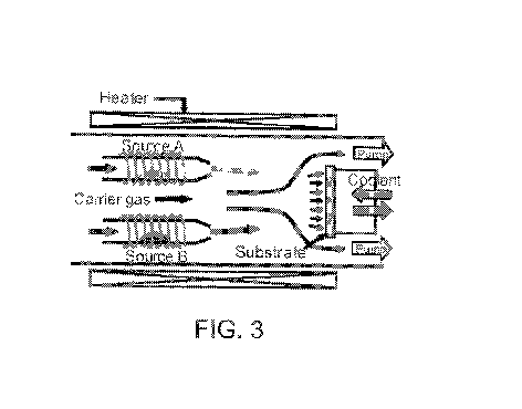
[0034] FIG. 3 is an illustration of an OVPD process according to one
embodiment of the
present disclosure.
[0035] FIG. 4a illustrates reflection high energy electron diffraction (RHEED)
patterns for
a bare KBr substrate with the electron beam pointed in the [100] direction.
[0036] FIG. 4b and FIG. 4c illustrate RHEED patterns along two different KBr
substrate
orientations for an approximately 40 nm layer thick PTCDA layer grown on its
surface.
[0037] FIG. 5 illustrates scanning electron microscope (SEM) images and
corresponding
RHEED patterns of 40 nm thick films of CuPc grown on highly oriented pyrolytic
graphite
7
CA 02696110 2010-02-10
WO 2009/029548 PCT/US2008/074120
(HOPG) as a function of temperature and reaction rate. The white scale bar
corresponds to
500 nm.
[0038] FIG. 6 on the left illustrates a RHEED pattern along the [100] KBr
direction for a
first 40 nm thick layer of PTCDA. In the middle is illustrated the RHEED
pattern for 15 nm
thick CuPc grown on the PTCDA layer. On the right is illustrated the surface
morphology of
the bilayer showing complete coverage but with an "orange peel" surface
morphology.
[0039] FIG. 7 depicts the hole mobility of 100 nm thick films of PTCDA
deposited at
various growth rates.
[0040] FIG. 8 illustrates an alternative process for making a heterojunction
according to
another embodiment of the present disclosure.
[0041] FIG. 9 is a schematic of a tandem cell.
Detailed Description
[0042] Thus, in one embodiment, there is disclosed a method of forming a layer
in an
organic photosensitive optoelectronic device, comprising: providing a
substrate; and growing
a thick crystalline layer of a first organic material on the substrate by
organic vapor phase
deposition, wherein said crystalline layer has crystallinity of long range
order, such as at least
0.25crri , at least 1.0crri , or at least 4.0crri . The crystalline layer is
at least about 150 A thick,
such as at least about 400 A thick.
[0043] In one embodiment, the method further comprising depositing a
crystalline layer of
a second organic material on the substrate, which may comprise an alkali-
halide material. In
one embodiment, the alkali-halide material comprises KBr. In another
embodiment, the
substrate comprises highly oriented pyrolytic graphite. In one embodiment, the
disclosed
substrate is maintained at a temperature ranging from -40 C to 90 C during
organic vapor
phase deposition.
[0044] In one embodiment, the disclosed method further comprising depositing a
self
assembled monolayer prior to growing said crystalline layer of a first organic
material on the
substrate. In one embodiment, the self assembled monolayer comprises an
alkanethiol.
[0045] It is understood that the first organic material may comprise a small
molecule or
polymeric material. Non-limiting examples of the small molecule material
include PTCDA
and CuPc. In one embodiment, the first organic material comprises CuPc, and
the second
organic material comprises PTCDA.
8
CA 02696110 2010-02-10
WO 2009/029548 PCT/US2008/074120
[0046] There is also disclosed an organic photosensitive device comprising at
least one
layer as disclosed herein, e.g., comprising a substrate, said substrate
comprising a crystalline
material of a first organic material, wherein the crystalline material has a
long-range
crystallinity order.
[0047] In one embodiment, the organic photosensitive device comprises at least
one layer
described herein that forms a heterojunction. There is also disclosed a method
of forming a
heterojunction for an organic photosensitive device. The method typically
comprises
growing a first crystalline layer of a first organic material on a substrate,
wherein the
substrate is maintained at a low temperature, such as one ranging from -40 C
to about 90 C;
growing a second oriented and crystalline layer of a second organic material
on the surface of
the first layer; wherein the first crystalline layer is an acceptor or donor
material and the
second crystalline layer is the opposite of the first crystalline layer.
[0048] In this embodiment, the method may comprise depositing a self-assembled
monolayer on the substrate prior to growing the first crystalline layer.
[0049] In another embodiment, the substrate is a stamp substrate and the
method further
comprises pressing the first and second crystalline layers and the self-
assembled monolayer
onto a first electrode. This embodiment may further comprise removing the
stamp substrate
and the self-assembled monolayer; and depositing an exciton blocking layer
over the first
crystalline layer. In addition, this method may further comprise depositing a
second
electrode over the exciton blocking layer.
[0050] As stated, in one embodiment, the first crystalline layer may comprise
CuPc and the
second crystalline layer may comprise C60. In another embodiment, the first
crystalline layer
may comprise CuPc and the second crystalline layer may comprise PTCDA.
[0051] In one embodiment, organic vapor phase deposition (OVPD) is used as the
primary means for the growth of crystalline organic films. OVPD differs from
previously
used vacuum techniques in that the organic molecules are evaporated into a
hot, inert
carrier gas which transports them through a hot walled reactor portion (to
prevent
deposition on the furnace itself) to a cooled substrate.
[0052] OVPD is different from the widely used vacuum thermal evaporation (VTE)
in that
OVPD uses a carrier gas to transport vapors into a deposition chamber.
Spatially separating
the functions of evaporation and transport leads to precise control over the
deposition
process, and enabling control over the organic surface morphology, e.g., flat
with smooth
surface or layers with protrusions. Another feature of OVPD, compared with
VTE, is the
9
CA 02696110 2010-02-10
WO 2009/029548 PCT/US2008/074120
large molecular surface diffusivity and the non-ballistic trajectories
followed by the
molecules in their arrival at the surface. OVPD is particularly effective at
filling preexisting
voids and other surface non-uniformities, whereas VTE is ineffective due to
the long mean
free paths and ballistic trajectories followed by incident molecules.
[0053] At typical deposition conditions used in OVPD, the flow of the carrier
gas around
the substrate creates a hydrodynamic boundary layer where molecular transport
is diffusion-
limited. The deposition rate, deposition efficiency, and film morphology are
controlled by
adjusting the organic species concentration, flow hydrodynamics, and surface
diffusivity.
[0054] In addition to improvements in carrier mobility, series resistance, and
overall
efficiency over spin-coat designs, the ordered nature of OVPD-grown
heterojunctions can
eliminate the occurrence of pockets of donor and acceptor material not
electrically connected
by a percolation pathway to an electrode.
[0055] A further advantage of OVPD over VTE is that (1) it is capable of
depositing
over very large substrate areas, and (2) it provides considerable control over
crystalline
morphology due to the ability to vary both ambient pressure and substrate
temperature.
Indeed, ambient gas pressure controls the surface mobility of adatoms, thereby
resulting
in control of surface texture as well as long range crystalline order.
[0056] Crystalline layers have drastically higher mobilities compared to their
disordered
counterparts (about 104 to about 106 times higher), thus leading to
significant increases in the
exciton diffusion length, layer conductivity, and resultantly, usable layer
thickness and
absorption efficiency. However, long range order of crystallinity in organic
films is
extremely difficult to achieve by methods other than the OVPD process
described herein;
thus, achieving layers with such drastically higher mobilities has been
elusive in the past.
Since IIEQE. depends on the product of individual efficiencies which are all
dependent on
charge mobility, achieving high crystallinity in the manner set forth herein
may have a
dramatic effect on the power conversion efficiency of a cell which uses such
crystalline films.
Finally, crystallinity over large areas should lead to more stable materials
by avoiding
metastable mixtures as represented by the bulk heterojunction architecture,
leading to PV
cells with practical operational lifetimes. Taken together, high efficiency
cells with areas > 4
crri can then be generated at low cost using the lightweight, flexible
substrates afforded by
the low processing temperatures characteristic of organic thin film materials.
[0057] In one embodiment, layers are "thick", in that they are extended into
their bulk
forms, and hence, continued growth of additional material would not change the
crystalline
CA 02696110 2010-02-10
WO 2009/029548 PCT/US2008/074120
habits or morphologies of the layers. In another embodiment, layers are at
least about 150 A
in thickness. In a further embodiment, layers are at least about 400 A in
thickness.
[0058] At least one formed layer should have long range crystalline order,
such as
crystalline order of at least about 0.25crri (0.5 cm by 0.5 cm), or at least
about 1.0crri (1.0
cm by 1.0 cm), or even at least about 4.0crri (2.0 cm by 2.0 cm).
[0059] In one embodiment at least one layer is oriented in the same direction
as an adjacent
layer.
[0060] In one embodiment, small molecule organic materials are used to make at
least
one layer. Non-limiting examples of such materials include CuPc, PTCDA, and
C60.
[0061] In one embodiment the substrate temperature in the OVPD is kept low,
for
example, at a temperatures ranging from -40 C to 90 C, or -40 C to 25 C.
[0062] Examples of EBLs are described in U.S. Patent No. 6,451,415 and
7,230,269 to
Forrest et al., which are incorporated herein by reference for their
disclosures related to
EBLs. Additional background explanation of EBLs may also be found in Peumans
et al.,
"Efficient photon harvesting at high optical intensities in ultrathin organic
double-
heterostructure photovoltaic diodes," Applied Physics Letters 76, 2650-52
(2000). EBLs
reduce quenching by preventing excitons from migrating out of the donor and/or
acceptor
materials.
[0063] A substrate may be any suitable substrate that provides desired
structural properties.
The substrate may be flexible or rigid, planar or non-planar. In some
embodiments, alkali
halide substrates are employed, such as KBr. In another embodiment, pyrolytic
graphite and
oriented pyrolytic graphite are also employed. In some embodiments, the
substrate may
comprise a thick crystalline layer of an organic material. The substrate may
be transparent,
translucent or opaque. Rigid plastics and glass are examples of rigid
substrate materials.
Flexible plastics and metal foils are examples of flexible substrate
materials. As illustrated in
FIG. 8, a self assembled monolayer cast onto a coinage metal, e.g., Au, Ag,
may be used as a
substrate. In one embodiment, the SAM comprises an alkanethiol. In another
embodiment, a
SAM is selected such that the bond strength between a film and anode (or an
ITO coated
anode, as illustrated in FIG. 8) is stronger than the film and a selected SAM,
so as to facilitate
transfer of a film from a SAM coated substrate.
[0064] An anode-smoothing layer may be situated between an anode layer and a
layer of a
heterojunction, such as a donor layer. Anode-smoothing layers are described in
U.S. Patent
11
CA 02696110 2010-02-10
WO 2009/029548 PCT/US2008/074120
6,657,378 to Forrest et al., incorporated herein by reference for its
disclosure related to this
feature.
[0065] Cells manufactured in accordance with the described embodiments may
comprise
additional organic layers that may be fabricated using vacuum deposition, spin
coating,
solution processing, organic vapor-phase deposition, inkjet printing, organic
vapor jet
printing and other methods known in the art. Organic materials may include
organometallic
compounds, including cyclometallated organometallic compounds.
[0066] A cell as illustrated in FIG. 9 may be connected to an element 608. If
the device is
a photovoltaic device, the element is a resistive load which consumes or
stores power. If the
device is a photodetector, element 608 is a current detecting circuit which
measures the
current generated when the photodetector is exposed to light, and which may
apply a bias to
the device (as described for example in Published U.S. Patent Application 2005-
0110007 Al,
published May 26, 2005 to Forrest et al.). If the rectifying junction is
eliminated from the
device (e.g., using a single photoconductive material as the photoactive
region), the resulting
structures may be used as a photoconductor cell, in which case the element 608
is a signal
detection circuit to monitor changes in resistance across the device due to
the absorption of
light. Unless otherwise stated, each of these arrangements and modifications
may be used for
the devices in each of the drawings and embodiments described herein.
[0067] An organic photosensitive optoelectronic device may also comprise
transparent
charge transfer layers, electrodes, or charge recombination zones. A charge
transfer layer
may be organic or inorganic, and may or may not be photoconductively active. A
charge
transfer layer is similar to an electrode, but does not have an electrical
connection external to
the device and only delivers charge carriers from one subsection of an
optoelectronic device
to the adjacent subsection. A charge recombination zone is similar to a charge
transfer layer,
but allows for the recombination of electrons and holes between adjacent
subsections of an
optoelectronic device. A charge recombination zone may include semi-
transparent metal or
metal substitute recombination centers comprising nanoclusters, nanoparticles,
and/or
nanorods, as described for example in U.S. Patent No. 6,657,378 to Forrest et
al.; Published
U.S. Patent Application 2006-0032529 Al, entitled "Organic Photosensitive
Devices" by
Rand et al., published February 16, 2006; and Published U.S. Patent
Application 2006-
0027802 Al, entitled "Stacked Organic Photosensitive Devices" by Forrest et
al., published
February 9, 2006; each incorporated herein by reference for its disclosure of
recombination
zone materials and structures. A charge recombination zone may or may not
include a
12
CA 02696110 2010-02-10
WO 2009/029548 PCT/US2008/074120
transparent matrix layer in which the recombination centers are embedded. A
charge transfer
layer, electrode, or charge recombination zone may serve as a cathode and/or
an anode of
subsections of the optoelectronic device. An electrode or charge transfer
layer may serve as a
Schottky contact.
[0068] In each of the devices described above, layers may be omitted, such as
the
smoothing layer and the exciton blocking layers. Other layers may be added,
such as
reflective layers or additional photoactive regions. The order of layers may
be altered or
inverted. A concentrator or trapping configuration may be employed to increase
efficiency,
as disclosed, for example in U.S. Patent No. 6,333,458 to Forrest et al. and
U.S. Patent No.
6,440,769 to Peumans et al., which are incorporated herein by reference.
Coatings may be
used to focus optical energy into desired regions of a device, as disclosed,
for example in
Published US Patent Application No. 2005-0266218 Al, entitled "Aperiodic
dielectric
multilayer stack" by Peumans et al., U.S. Patent No. 7,196,835, which is
incorporated herein
by reference. In the tandem devices, transparent insulative layers may be
formed between
cells, with the electrical connection between the cells being provided via
electrodes. Also in
a tandem cell, one or more of the photoactive regions may be a Schottky-
barrier
heterojunction instead of a donor-acceptor heterojunction. Arrangements other
than those
specifically described may be used.
Definitions
[0069] Electrodes, such as anodes and cathodes, may be composed of metals or
"metal
substitutes." Herein the term "metal" is used to embrace both materials
composed of an
elementally pure metal, and also metal alloys which are materials composed of
two or more
elementally pure metals. The term "metal substitute" refers to a material that
is not a metal
within the normal definition, but which has the metal-like properties such as
conductivity,
such as doped wide-bandgap semiconductors, degenerate semiconductors,
conducting oxides,
and conductive polymers. Electrodes may comprise a single layer or multiple
layers (a
"compound" electrode), may be transparent, semi-transparent, or opaque.
Examples of
electrodes and electrode materials include those disclosed in U.S. Patent No.
6,352,777 to
Bulovic et al., and U.S. Patent No. 6,420,031, to Parthasarathy, et al., each
incorporated
herein by reference for disclosure of these respective features. As used
herein, a layer is said
to be "transparent" if it transmits at least 50% of the ambient
electromagnetic radiation in a
relevant wavelength.
13
CA 02696110 2010-02-10
WO 2009/029548 PCT/US2008/074120
[0070] As used herein, the term "organic" includes polymeric materials as well
as small
molecule organic materials that may be used to fabricate organic
optoelectronic devices.
"Small molecule" refers to any organic material that is not a polymer, and
"small molecules"
may actually be quite large. Small molecules may include repeat units in some
circumstances. For example, using a long chain alkyl group as a substituent
does not remove
a molecule from the "small molecule" class. Small molecules may also be
incorporated into
polymers, for example as a pendent group on a polymer backbone or as a part of
the
backbone. Small molecules may also serve as the core moiety of a dendrimer,
which consists
of a series of chemical shells built on the core moiety. The core moiety of a
dendrimer may
be a fluorescent or phosphorescent small molecule emitter. A dendrimer may be
a "small
molecule." In general, a small molecule has a defined chemical formula with a
molecular
weight that is the same from molecule to molecule, whereas a polymer has a
defined
chemical formula with a molecular weight that may vary from molecule to
molecule. As
used herein, "organic" includes metal complexes of hydrocarbyl and heteroatom-
substituted
hydrocarbyl ligands.
[0071] As used herein, a first HOMO or LUMO energy level is "greater than" or
"higher
than" a second HOMO or LUMO energy level if the first energy level is closer
to the vacuum
energy level 10. A higher HOMO energy level corresponds to an ionization
potential ("IP")
having a smaller absolute energy relative to a vacuum level. Similarly, a
higher LUMO
energy level corresponds to an electron affinity ("EA") having a smaller
absolute energy
relative to vacuum level. On a conventional energy level diagram, with the
vacuum level at
the top, the LUMO energy level of a material is higher than the HOMO energy
level of the
same material.
[0072] The term "organometallic" as used herein is as generally understood by
one of
ordinary skill in the art and as given, for example, in Chapter 13 of
"Inorganic Chemistry"
(2nd Edition) by Gary L. Miessler and Donald A. Tarr, Prentice Hall (1999).
[0073] The term "highly oriented pyrolytic graphite" refers to a graphite
material having a
mosaic spread of less than 1 degree.
[0074] The term "long range order" as used herein generally refers to the
order observed
across a substrate of at least 1 square micron, or even several square microns
(urn ), or in
some cases, at least 0.5mrn .
14
CA 02696110 2010-02-10
WO 2009/029548 PCT/US2008/074120
Examples
[0075] Specific examples of the invention are illustrated and/or described
herein.
However, it will be appreciated that modifications and variations of the
invention are covered
by the above teachings and within the purview of the appended claims without
departing
from the spirit and scope of the invention.
General OVPD Process
[0076] A non-limiting example of an OVPD system schematic is shown in FIG. 3.
In
OVPD a hot inert carrier gas 1 is infused with an evaporated organic 2 which
emanates
from source cell 3. The organic 2 is transported to a cooled substrate 4 where
deposition
occurs, thus forming film 5. Gas temperature, substrate temperature, and gas
pressure can
be varied to affect the crystallinity of film 5.
[0077] In one embodiment, in situ diagnostics can be used to monitor the
crystallinity
of the film 5, such as reflection high energy electron diffraction (RHEED), a
technique
which is commonly used in ultrahigh vacuum systems such as organic molecular
beam
deposition (OMBD).
[0078] A non-limiting example of the ability of OVPD to achieve long range
crystalline
order is demonstrated by the growth of an archetype molecular crystal of
3,4,9,10
perylenetetracarboxylic dianhydride (PTCDA) on a single crystal of KBr. Growth
was
carried out in a vertical, multibarrel quartz OVPD chamber described
previously. See
Shtein et al., T. Appl. Phys., vol. 89, p. 1470 (2001), incorporated herein by
reference.
Crystal structure was monitored in situ and in real-time with HP-RHEED (see
Lunt et al.,
Appl. Phys. Lett., 2007, 70, incorporated herein by reference), and ex situ
with x-ray
diffraction in the Bragg-Brentano configuration using a Rigaku Cu-Ka rotating
anode
source. HP-RHEED patterns using a 0.1x20 mm2 electron beam were recorded at a
beam
energy, current, and incident angle of 20keV, <100nA, and -1 , respectively.
Beam
current was minimized to avoid charging at >100nA. Film thickness was measured
post-
growth using a variable-angle spectroscopic ellipsometer on solvent-cleaned Si
substrates.
Surface topography was observed using scanning electron microscopy (SEM) after
coating the surface with 20A of Au to prevent charging.
[0079] PTCDA was twice purified by gradient sublimation prior to loading into
a quartz
source boat located in a barrel of the OVPD chamber. PTCDA was evaporated at
385 C
at a 25 sccm nitrogen flow, corresponding to a nominal deposition rate of 0.7
A/s at a
CA 02696110 2010-02-10
WO 2009/029548 PCT/US2008/074120
growth pressure of 60mTorr. Single crystal KBr substrates were cleaved
immediately
prior to being loaded into the growth chamber.
[0080] To index the HP-RHEED patterns, the d-spacings were calculated for each
assigned streak location, calibrated using the KBr pattern. X-ray diffraction
was used to
determine the stacking direction of the film to help identify in-plane surface
meshes.
Lattice constants were fit to the d-spacings, and assigned indices using a non-
linear least
squares regression of all the data.
[0081] FIG. 4a depicts a RHEED pattern for a bare KBr substrate with the
electron
beam oriented in the [100] direction.
[0082] The resulting RHEED pattern of a 400 A thick PTCDA film are shown in
FIG.
4b and FIG. 4c along two KBr crystalline directions. Streak locations are
highlighted
with white tick marks. The well defined and continuous streaks in the RHEED
pattern
indicate a flat and well ordered structure over the length of the probing
electron beam, or
over approximately 0.1 mm x 2 cm. The measured d-spacings for FIG. 4b are
(02), (20) _
9.7A, 6.OA, respectively. The measured d-spacings for FIG. 4c are (11), (12),
(14), (24),
(26), (28), (55), (66) = 10.4A, 7.9A, 4.7A, 3.9 A, 2.96 A, 2.29 A, 2.10A, 1.72
A,
respectively. Indexing of the streaks (as indicated by the short white lines
with unit mesh
indices noted) clearly indicates that PTCDA is growing in its relaxed a-phase.
Furthermore, the variation of streak pattern along the (110) and (100) KBr
directions
clearly shows a preferred alignment to the underlying crystal. This is
remarkable since
there is no apparent lattice match between the PTCDA and KBr structures, where
the
strain exceeds 5%. This ability to grow ordered, but relaxed molecular
crystals on
substrates without matching is believed to be a direct result of the "soft"
van der Waals
bonds characteristic of organic materials. This property has been studied
extensively in
laboratories around the world, and is known as "quasi-epitaxy". Of particular
note is the
nearly perfect alignment over such a large, macroscopic region for this
particular
film/substrate combination. The overall dimensions of the ordered PTCDA film
were
12mm x 25mm, and the film was about 1mm thick. It is believed that this degree
of film
crystal perfection has not been observed for a thick film over such large
dimensions.
[0083] In FIG. 5 is shown a matrix of substrate temperatures and background
reactor
pressures on the crystalline morphology of a donor material, copper
phthalocyanine
(CuPc) grown on highly oriented pyrolytic graphite (HOPG). There is clearly a
significant degree of control over crystal parameters over the range of growth
parameters.
16
CA 02696110 2010-02-10
WO 2009/029548 PCT/US2008/074120
Again, quasi-epitaxial alignment of film to substrate is observed under some
growth
conditions.
[0084] In another non-limiting example, a crystalline layer of a first
organic, PTCDA, was
grown on a substrate, KBr, followed by the growth of a second oriented and
crystalline layer
of a second organic material, CuPc, on the surface of the PTCDA. The RHEED
patterns and
morphology of the first and second layers are shown in FIG. 6. Both layers are
"thick" in that
they are extended into their bulk forms, and hence, continued growth of
additional material
would not change the crystalline habits or morphologies of the layers. The
PTCDA layer has
a thickness of 40 nm, and the CuPc layer has a thickness of 15 nm. It is
believed that this is
the first demonstration of the growth of a bulk crystalline organic material
on top of another,
forming a fully ordered planar heterojunction (hereinafter, an "organic
crystalline planar
heterojunction")
[0085] The above examples clearly indicate that films having long range order
of
crystallinity can be achieved using small molecule organic materials under the
favorable
growth conditions afforded by OVPD. Furthermore, charge mobility is a strong
function of
order. As shown in FIG. 7, hole mobility in PTCDA is shown as a function of
growth rate.
FIG. 7 demonstrates that mobility increases by two orders of magnitude,
reaching a
maximum of 1.5 crri /(V=s) at a rate of 50 A/s when grown in ultrahigh vacuum.
This
increased mobility has also been observed in pentacene grown by OVPD. See M.
Shtein, J.
Mapel, J. B. Benziger, and S. R. Forrest, "Effects of film morphology and gate
dielectric
surface preparation on the electrical characteristics of organic vapor phase
deposited
pentacene thin-film transistors", Appl. Phys. Lett., vol. 81, p. 268 (2002),
herein incorporated
by reference. Hence, such heterojunctions in PV cells, including organic
crystalline planar
heterojunctions, should be expected to have very high power conversion
efficiencies.
General Method for Manufacturing a PV Cell
[0086] In accordance with another embodiment, an exemplary method of
manufacturing a
PV cell is provided comprising the steps of: a) deposition, by OVPD, of the
donor-acceptor
heterojunction on a stamp with a pre-deposited self assembled monolayer (SAM)
on Au to
form the growth template; b) transfer by stamping the crystalline
heterojunction onto an
indium tin oxide (ITO) coated substrate; c) thus, forming a complete
heterojunction, upon
which; d) an exciton blocking layer (EBL) and a metal cathode is deposited to
complete the
cell. Details of this non-limiting process are depicted in FIG 8(a) through
FIG. 8(d),
respectively.
17
CA 02696110 2010-02-10
WO 2009/029548 PCT/US2008/074120
[0087] By repeating process steps as depicted in FIG. 8(a) and FIG. 8(b), more
complex
cells, such as the exemplary tandem (or "stacked") device depicted in FIG. 9,
may be formed.
A non-limiting example of a organic photosensitive optoelectronic cell with
multiple organic
layers, or a multilayer device 600, is shown in FIG. 9. Insulating or
conducting substrate 601
supports the device. First electrode 602 comprises, e.g., ITO of an
appropriate thickness.
The non-limiting exemplary device also includes organic layers 603, 604, 605,
and 606.
Finally, second transparent electrode 607 is adjacent to organic layer 606.
[0088] In a tandem cell, heterojunctions having various layer thicknesses may
be stacked
to optimize the absorption of various wavelengths of light. In one embodiment,
a tandem cell
is formed by first forming at least a heterojunction as depicted in FIG. 8(c),
wherein the
substrate used is transparent glass, wherein the anode on the substrate is
ITO, and wherein the
heterojunction (or heterojunctions, such as a double heterojunction) has layer
thicknesses
which selectively absorb red light. Next, a second heterojunction is stamped
upon the first
heterojunction, where in the second heterojunction has layer thicknesses which
preferably
absorb blue light. Last, a cathode is deposited on the second heterojunction
(much as
depicted in FIG. 8(d)), and the tandem cell is completed.
[0089] Transparent charge transfer layers, electrodes, or charge recombination
zones may
also be included in a tandem cell. For example, a silver nanoparticle layer
(not depicted) may
be used between the first heterojunction and the second heterojunction to
intensify the optical
field in adjacent absorbing layers, while simultaneously acting as
recombination sites for
photogenerated electrons and holes.
[0090] The examples set forth above set forth exemplary embodiments of the
invention,
but unless expressly specified, are not intended to set limits on the
invention.
[0091] Unless otherwise indicated, all numbers expressing quantities of
ingredients,
reaction conditions, and so forth used in the specification and claims are to
be understood as
being modified in all instances by the term "about." Accordingly, unless
indicated to the
contrary, the numerical parameters set forth in the following specification
and attached
claims are approximations that may vary depending upon the desired properties
sought to be
obtained by the present invention.
[0092] Specific examples of the invention are illustrated and/or described
herein.
However, it will be appreciated that modifications and variations of the
invention are covered
by the above teachings and within the purview of the appended claims without
departing
from the spirit and scope of the invention.
18