Note: Descriptions are shown in the official language in which they were submitted.
CA 02698506 2010-03-04
WO 2009/032274 PCT/US2008/010367
FIBER OPTIC SYSTEM FOR ELECTROMAGNETIC SURVEYING
Cross-reference to related applications
Not applicable.
Statement regarding federally sponsored research or development
Not applicable.
Background of the Invention
Field of the Invention
[0001] The invention relates generally to the field of electromagnetic
surveying of the
Earth's subsurface. More specifically, the invention relates to
electromagnetic survey
systems including optical output sensors to reduce effects of electromagnetic
noise on
signals measured by the system.
Background Art
[0002] Electromagnetic geophysical surveying of the Earth's subsurface
includes
"controlled source" and "natural source" electromagnetic surveying. Controlled
source electromagnetic surveying includes imparting an electric field or a
magnetic
field into subsurface Earth formations, such formations being below the sea
floor in
marine surveys, and measuring electric field amplitude and/or amplitude of
magnetic
fields induced in response to the imparted field. Such measurements are
performed
by measuring voltage differences induced between spaced apart electrodes,
induced in
antennas and/or interrogating magnetometers disposed at the Earth's surface,
or near
or above the sea floor. The electric and/or magnetic fields from which the
above
measurements are made are induced in response to the electric field and/or
magnetic
field imparted into the Earth's subsurface, as stated above, and inferences
about the
spatial distribution of electrical conductivity of the Earth's subsurface are
made from
recordings of the induced electric and/or magnetic field measurements.
[0003] Natural source electromagnetic surveying includes deploying multi-
component ocean bottom receiver stations and by taking the ratio of
perpendicular
1
CA 02698506 2010-03-04
WO 2009/032274 PCT/US2008/010367
field components, one can eliminate the need to know characteristics of the
natural
source.
[0004] Controlled source electromagnetic surveying known in the art includes
imparting alternating electric current into the subsurface formations. The
alternating
current has one or more selected frequencies. Such surveying is known as
frequency
domain controlled source electromagnetic (f-CSEM) surveying. Another technique
for electromagnetic surveying of subsurface Earth formations known in the art
is
transient controlled source electromagnetic surveying (t-CSEM). In t-CSEM,
electric
current is imparted into the Earth at the Earth's surface (or sea floor), in a
manner
similar to f-CSEM. The electric current may be direct current (DC). At a
selected
time, the electric current is switched off, switched on, or has its polarity
changed, and
induced voltages and/or magnetic fields are measured, typically with respect
to time
over a selected time interval, at the Earth's surface or water surface.
Alternative
switching techniques are possible. Structure of the subsurface is inferred by
the time
distribution of the induced voltages and/or magnetic fields. For example, U.S.
Patent
Application Publication No. 2004/232917 and U.S. Patent No. 6,914,433
Detection of
subsurface resistivity contrasts with application to location of fluids
(Wright, et al)
describes a method of mapping subsurface resistivity contrasts by making
multichannel transient electromagnetic (MTEM) measurements on or near the
Earth's
surface using at least one source, receiving means for measuring the system
response
and at least one receiver for measuring the resultant earth response. All
signals from
each source-receiver pair are processed to recover the corresponding
electromagnetic
impulse response of the earth and such impulse responses, or any
transformation of
such impulse responses, are displayed to create a subsurface representation of
resistivity contrasts. The system and method enable subsurface fluid deposits
to be
located and identified and the movement of such fluids to be monitored.
[0005] The above methods for f-CSEM and t-CSEM have been adapted for use in
marine environments. Cable based sensors have been devised for detecting
electric
and/or magnetic field signals resulting from imparting electric and/or
magnetic fields
into formations below the bottom of a body of water. See, for example, U.S.
Patent
Application Publication No. 2006/0238200 filed by Johnstad. The amplitude of
electric field signals detected by electrodes on cables such as described in
the
2
CA 02698506 2010-03-04
WO 2009/032274 PCT/US2008/010367
Johnstad publication may be on the order of fractions of a nanovolt.
Accordingly, a
particular consideration in the design and implementation of electromagnetic
survey
receiver systems is reducing the amount of noise that may be induced in the
signals
detected by the various sensing elements in the receiver system. One example
of such
noise reduction is to include batteries at each of a plurality of receiver
system stations
where signal amplification devices may be located. By eliminating the need to
transmit operating power along a cable associated with the receiver system,
induced
noise may be reduced. Battery power does not eliminate induced noise resulting
from
electrical signal telemetry in cable type systems such as shown in the
Johnstad
publication, however, because electric current carrying such signals,
representative of
the voltages and/or magnetic field amplitudes measured, may induce noise in
the
measured signals.
[0006] There is a continuing need for electromagnetic survey devices that
reduce
noise induced in the measured signals caused by electric power and signal
transmission along receiver cables.
Summary of the Invention
[0007] An electromagnetic survey sensing device according to one aspect of the
invention includes at least two electrodes disposed at spaced apart locations.
An
electrical to optical converter is electrically coupled to the at least two
electrodes.
The converter is configured to change a property of light from a source in
response to
voltage imparted across the at least two electrodes. The device includes an
optical
fiber optically coupled to an output of the electrical to optical converter,
the optical
fiber in optical communication with a detector.
[0008] An electromagnetic survey system according to another aspect of the
invention
includes a receiver cable having an optical fiber associated therewith and
coupled at
one end to a recording device and at another end to at least one electrical to
optical
converter. The recording device includes a light source and a photodetector
therein in
optical communication with the associated fiber. At least two electrodes are
disposed
at spaced apart locations along the receiver cable. The electrical to optical
converter
is electrically coupled to the at least two electrodes. The converter is
configured to
change a property of light from the source in response to voltage imparted
across the
3
CA 02698506 2010-03-04
WO 2009/032274 PCT/US2008/010367
at least two electrodes. The optical fiber is optically coupled to an output
of the
electrical to optical converter. The optical fiber is in optical communication
with the
detector in the recording device.
[0009] A method for sensing an electromagnetic field according to another
aspect of
the invention includes exposing an electric dipole antenna to the
electromagnetic
field. Voltage imparted to the antenna is conducted to an electrical device
that
changes a property of light imparted thereto in response to the voltage. A
property of
light conducted from a light source to the device and from the device to a
photodetector along an optical fiber is varied, so that a signal corresponding
to the
voltage is optically communicated to the photodetector.
[0010] An electromagnetic survey system according to another aspect of the
invention
includes a survey vessel configured to tow a receiver cable through a body of
water.
The system includes a receiver cable having an optical fiber associated
therewith and
coupled at one end to a recording device on the vessel and at another end to a
plurality
of optical magnetic field sensors disposed at spaced apart positions along the
cable.
The sensors are each configured to change a property of light from source
associated
with the recording device. A signal detector is associated with the recording
device
and is configured to convert the changed property of light into a signal
corresponding
to a property of a magnetic field proximate each sensor.
[0011] A method for electromagnetic surveying of formations in the Earth's
subsurface includes imparting an electromagnetic field into the formations. A
magnetostrictive material is exposed to an electromagnetic field produced in
response
to the imparted electromagnetic field. A change in dimension of the
magnetostrictive
material caused by the responsively produced field is transferred to an
optical fiber.
The transferring causes a change in a property of light conducted from a light
source
to a photodetector along the optical fiber, so that a signal corresponding to
the
responsively produced electromagnetic field is optically communicated to the
photodetector.
[0012] Other aspects and advantages of the invention will be apparent from the
following description and the appended claims.
4
CA 02698506 2010-03-04
WO 2009/032274 PCT/US2008/010367
Brief Description of the Drawings
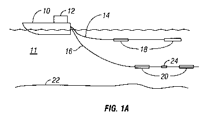
[0013] FIG. 1 A shows an example marine electromagnetic survey system having a
towed receiver cable.
[0014] FIG. 1 B shows an example marine electromagnetic survey system
including
an ocean bottom receiver cable.
[0015] FIG. 2A shows one example electrical to optical converter that can be
used
with the systems shown in FIG. 1 A and FIG. 1 B.
[0016] FIG. 2B shows light source and signal detection components of a
recording
system as in FIG. 1 that may be used with various examples of a system
according to
the invention.
[0017] FIGS. 3 through 6 show other examples of devices that can change a
length of
an optical path in response to a voltage imparted across electrodes.
[0018] FIGS. 7A and 7B shown an example of a magnetic field sensing system
using
fiber optic sensors.
Detailed Description
[0019] An example electromagnetic survey system is shown schematically in FIG.
1 A. The system shown in FIG. 1A is intended for marine use, however it will
be
appreciated by those skilled in the art that the invention is equally
applicable to land-
based electromagnetic surveys. A survey vessel 10 moves along the surface of a
body
of water 11 such as a lake or the ocean. The vessel 10 may include equipment,
shown
generally at 12 and referred to for convenience as a "recording system" that
includes
devices (none shown separately) for applying electric current to a source
cable 14
towed by the vessel, for navigating the vessel and for recording signals
detected by
one or more sensors on a receiver cable 16.
[0020] The source cable 14 in the present example includes two source
electrodes 18
disposed at spaced apart positions along the source cable 14. At selected
times the
equipment (not shown separately) in the recording system 12 conducts electric
current
across the source electrodes 18. Such electric current produces an
electromagnetic
field that propagates through the water 11 and into the formations below the
water
CA 02698506 2010-03-04
WO 2009/032274 PCT/US2008/010367
bottom 22. The particular type of current conducted across the source
electrodes 18
may be single- or multi-frequency alternating current, or various forms of
switched
direct current, such that either or both transient and frequency domain
controlled
source electromagnetic surveying may be performed. It should also be
understood
that the arrangement of source electrodes 18 shown in FIG. 1A, referred to as
a
horizontal electric dipole transmitter antenna, is not the only type of
electromagnetic
transmitter that may be used with the invention. The source cable 14 could
also tow,
in addition to or in substitution of the horizontal electric dipole
transmitter antenna
shown in FIG. 1A, any one or more of a vertical electric dipole antenna, and
horizontal or vertical magnetic dipole antenna. Accordingly, the source
antenna
configuration shown in FIG. 1 A is not intended to limit the scope of the
invention.
[0021] In the example shown in FIG. lA, the vessel 10 also tows a receiver
cable 16.
The receiver cable 16 includes at least one pair of electrodes 20 disposed at
spaced
apart positions along the receiver cable 16. An electric field resulting from
interaction
of the induced electromagnetic field in the formations below the water bottom
22
induces voltages across the at least one pair of electrodes 20. In the present
example,
the pair of electrodes 20 may be associated with an electrical to optical
converter 24
disposed at a selected position along the receiver cable 16, typically, but
not
necessarily between the electrodes 20. The electrical to optical converter 24
generates
an optical signal that is related to the voltage induced across the electrodes
20 in
response to the electromagnetic field imparted by the transmitter antenna
(source
electrodes 18). The optical signal is transmitted along an optical fiber (see
27 in FIG.
2A) associated with the receiver cable 16 to the recording unit 12, or as will
be
explained below with reference to FIG. 1 B to a recording device.
[0022] FIG. 1 B shows an arrangement similar to that of FIG. 1 A, however, the
receiver cable 16A is deployed on the water bottom 22. The receiver cable 16A
in
FIG. 1 B may include at least one pair of electrodes 20A and an electrical to
optical
converter 24A associated therewith similar to those shown in FIG. 1 A. The
receiver
cable 16A in FIG. 1 B may have a recording device 17 associated therewith to
record
signals produced by the electrical to optical converter 24A and transmitted
along an
optical fiber (see FIG. 2A) from the converter 24A to the recording device 17.
During
acquisition using a receiver cable on the water bottom such as shown in FIG. 1
A,
6
CA 02698506 2010-03-04
WO 2009/032274 PCT/US2008/010367
there is typically no direct electrical or other type of connection between
the receiver
cable 16A and the recording system 12 on the vessel 10, thus it is convenient
to
provide a recording device 17 associated with the receiver cable 16A. Other
than the
manner of deployment of the receiver cable 16A, acquisition of electromagnetic
signals may be similar to that explained above with reference to FIG. lA.
[0023] An example of an electrical to optical converter 24 is shown in more
detail in
FIG. 2A. The electrical to optical converter 24 may include a piezoelectric
element or
crystal 28 that is electrically coupled to each of the electrodes 20. When the
piezoelectric element 28 is so coupled to the electrodes 20, any voltage
imparted
across the pair of electrodes 20 will be conducted to the piezoelectric
element 28. The
piezoelectric element 28 will change shape to an extent corresponding to the
voltage
imparted across the electrodes 20. The piezoelectric element 28 may be in a
convenient shape such as a cylinder that is configured to change diameter in
response
to the imparted voltage. The piezoelectric element 28 may be made from
piezoelectric materials having high charge constants and high electro-
mechanical
coupling coefficients, such as lead zirconate titanate ("PZT"), lead magnesium
niobate-lead titanate ("PMN-PT") and lead zirconate niobate-lead titanate
("PZN-
PT").
[0024] An optical interferometer, which in the present example may include an
optical coupling 26, a sensing fiber 30 and a reference fiber 32 coupled to
output
terminals of the optical coupling 26 may be arranged as shown in FIG. 2A. The
sensing fiber 30 may be wound around the piezoelectric element 28 such that
change
in dimensions of the piezoelectric element 28, related to the voltage across
the
electrodes 20, will cause a corresponding change in the length of the sensing
fiber 30.
The reference fiber 32 may be provided such that changes in ambient conditions
(e.g.,
temperature, pressure) will substantially equally affect both the sensing
fiber 30 and
the reference fiber 32. Each of the fibers 32, 30 may be terminated at an end
opposite
the optical coupling 26 by a mirror 39. The combination of optical elements
shown in
FIG. 2A may result in a phase shift in light passing through the sensing fiber
30,
which when combined with light passing through the reference fiber 32 may
produce
an optical phase shift in the first optical coupling 26. The phase information
may be
conducted along an optical fiber 27 to the detection equipment (e.g. in the
recording
7
CA 02698506 2010-03-04
WO 2009/032274 PCT/US2008/010367
device 17 in FIG. 1 B or in the recording system 12 in FIG. IA) where the
optical
phase can be demodulated to reconstruct a signal corresponding to the imparted
voltage with respect to time.
[0025] An example of a light source and detection devices used in association
with
the recording unit (12 in FIG. lA) or the recording device (17 in FIG. 1B)
will new be
explained with reference to FIG. 2B. In FIG. 2B, a light source 34 such as a
laser
diode may provide light at one or more wavelengths to the optical fiber 27
associated
with the receiver cable (e.g., 16 in FIG. 1A). The light source 34 may be
disposed in
the recording system 12, if a towed receiver cable is used, or may be disposed
in the
recording device (17 in FIG 1 B) if the receiver cable (e.g., 16A in FIG. 1 B)
is
disposed on the water bottom. The output of the light source 34 may pass
through a
modulator 36 to cause the light to be modulated, for example, to be pulsed at
one or
more selected frequencies. Output of the modulator 36 may be conducted to an
optical coupling 42, one output of which is coupled to the optical fiber 27. A
return
tap on the optical coupling 42 may be coupled to a photodetector 40, which
converts
the returning light into an electrical signal corresponding to the amplitude
of the light.
Output of the photodetector 40 may be coupled to a demodulator 38 to recover
the
signals from the electrical to optical converter (e.g., 24 in FIG. 2A)
[0026] The general principle of the electrical to optical converter (24 in
FIG. 2A) is to
convert a voltage imparted across the electrodes (20 in FIG. 2A) to a
corresponding
change in properties of light from the source (34 in FIG. 2B). The change in
properties of the light caused by the converter is such that a signal
corresponding to
the imparted voltage may be optically communicated to the recording system or
the
recording device without the need for electrical power to be transmitted along
the
receiver cable either as operating power or as signal telemetry. One type of
change in
properties of the light from the source is to cause a phase shift in the
light. In such
examples, the phase shift is related to the length of an optical path along
the sensing
fiber and/or optical components associated with the sensing fiber. The
electrical to
optical converter elements shown in FIG. 2A, for example cause a change in
length of
the optical path through the sensing fiber (30 in FIG. 2A) by changing the
fiber length
corresponding to change in diameter of the piezoelectric element (28 in FIG.
2A) as
explained above.
8
CA 02698506 2010-03-04
WO 2009/032274 PCT/US2008/010367
[0027] Other examples of electrical to optical converters that can change the
length of
an optical path in response to a voltage imparted across the electrodes (20 in
FIG. 2A)
will now be explained with reference to FIGS. 3 through 6.
[0028] In FIG. 3, the converter 24 can include a cylindrically shaped
piezoelectric
element or crystal 28 as in the previous examples. The piezoelectric element
28 may
be etched or otherwise have a feature 28A approximately in its longitudinal
center
that causes one longitudinal segment of the piezoelectric element 28 to
operate
independently of the other longitudinal segment. A first sensing fiber 30A may
be
wound around one longitudinal segment, and a second sensing fiber 32A may be
wound around the other longitudinal segments of the piezoelectric element 28.
The
sensing fibers 30A, 32A may each include a mirror 39 or similar reflective
surface at
the terminal ends thereof, and may be coupled at the opposite ends thereof to
an
optical coupling as in FIG. 2A. The two longitudinal segments of the
piezoelectric
element or crystal 28 are electrically coupled to the electrodes (20 in FIG.
2A) in
opposed polarity as shown in FIG. 3. Arranged as shown in FIG. 3, one
longitudinal
segment of the piezoelectric element 28 will contract in diameter and the
other
segment will expand in diameter when a voltage is imparted across the
electrodes (20
in FIG. 2A). Therefore, one sensing fiber will increase length and the other
will
decrease length. When the fibers 30A, 28A change length, an interference
pattern
may be generated in the optical coupling 26. The arrangement shown in FIG. 3
may
thus provide increased sensitivity because of the opposite change in length of
each
sensing fiber 30A, 28A in response to voltage imparted across the electrodes
(20 in
FIG. 1 A). The principle of the device shown in FIG. 3 may also be implemented
by
using two separate piezoelectric elements electrically coupled to the
electrodes in
opposite polarity.
[0029] Another example shown in FIG. 4 may include a sensing fiber 30 and a
reference fiber 32 as in the example of FIG. 2A. The example of FIG. 4 may
include
a piezoelectric element 28A including a stack of piezoelectric wafers disposed
proximate the terminal end of the sensing fiber 30. A collimating lens 29 may
be
fixed to the end of the sensing fiber 30. One side of the piezoelectric
element 28A
may include a mirror 28B facing the lens 29. The piezoelectric element 28A is
electrically coupled to the electrodes (20 in FIG. 2A) such that a voltage
imparted
9
CA 02698506 2010-03-04
WO 2009/032274 PCT/US2008/010367
across the electrodes changes the length of the piezoelectric element 28A and
correspondingly changes a distance between the mirror 28B and the lens 29.
Changing the foregoing distance changes the optical path length of the sensing
fiber,
and results in an interference pattern in an optical coupling 26, which is
coupled to
both the sensing fiber 30 and the reference fiber 32. The reference fiber 32
may itself
include a mirror 39 at the terminal end thereof to reflect light back to the
optical
coupling 26 for creating the interference patter with light from the sensing
fiber.
[0030] Another example of an electrical to optical converter is shown in FIG.
5 that is
similar in operating principle to the example shown in FIG. 4. In the example
of FIG.
5, a first sensing fiber 30B is arranged as part of an interferometer
substantially as
explained above with reference to FIG. 4 and is electrically coupled to the
electrodes
(20 in FIG. 2A) so that the element 28A changes length in response to voltage
imparted across the electrodes (20 in FIG. 2A). Rather than using a reference
fiber as
in FIG. 4, the example of FIG. 5 includes a second sensing fiber 32B that has
a
collimating lens 29 at the terminal end thereof. A piezoelectric element 28A
with
mirror 28B thereon, similar to the piezoelectric element proximate the end of
the first
sensing fiber 30A, is disposed proximate the end of the second sensing fiber
32A.
The piezoelectric element 28A proximate the end of the second sensing fiber is
electrically coupled to the electrodes (20 in FIG. 2A) in opposed polarity to
the
coupling of the element 28A proximate the first sensing fiber 30A. Thus, a
voltage
imparted across the electrodes (20 in FIG. 2A) causes the two piezoelectric
elements
28A to oppositely change length. The optical path length of the first sensing
fiber
30A changes length in an opposite manner to the change in length of the second
sensing fiber 32A. The arrangement shown in FIG. 5 may have increased
sensitivity
as compared to the arrangement shown in FIG. 4.
[0031] Another example of an electrical to optical converter is shown in FIG.
6. The
sensing fibers 30C, 32C forming part of an optical interferometer as in the
previous
examples may each include a micro electromechanical sensing material, such as
a
lithium niobate etched into each fiber as shown at 40. Each etching has a
mirror (not
show separately) associated therewith. The etchings 40 may be electrically
coupled
proximate the ends thereof to the electrodes (20 in FIG. 2A). When voltage is
imparted across the electrodes, the etchings 40 will change length, and
thereby move
CA 02698506 2010-03-04
WO 2009/032274 PCT/US2008/010367
the associated mirror. Such movement will change the optical path length of
each
fiber 30C, 32C so that an interference pattern may be generated in the optical
coupling 26.
[0032] The foregoing examples are directed to electric field sensors that
convert
voltage imparted across spaced apart electrodes into a change in optical
properties of
light passed through an optical fiber. In other examples, described below with
reference to FIG. 7A and FIG. 7B, a magnetic field resulting from imparting an
electromagnetic field into the subsurface formations may be detected using a
magnetostrictive sensor associated with an optical fiber. First referring to
FIG. 7A, a
survey system that is configured similarly to the system shown in FIG. 1 A
includes a
survey vessel 10 including a recording system 12 thereon. The vessel 10 tows
at least
one electromagnetic receiver cable 16 according to the present example. The
receiver
cable 16 may include a plurality of spaced apart magnetostrictive sensors 24A
at
spaced apart positions along the receiver cable 16. An electromagnetic field
source
(not shown in FIG. 7A) may be towed by the vessel 10 or by another vessel (not
shown).
[0033] The sensors 24A respond to changes in the amplitude of a magnetic field
by
changing a dimension of a magnetostrictive material. Such dimensional change
causes a corresponding change in a dimension of an optical fiber.
[0034] Referring to FIG. 7B, a sensing fiber 32 and a reference fiber 30 form
two
arms of an interferometer. Such interferometer may operate similarly to the
example
shown and explained with reference to FIG. 4, although such example is not a
limit on
the scope of this invention. The sensing fiber 32 may be coupled to a
magnetostrictive material 132 such than changes in magnetic field proximate
the
magnetostrictive material cause change in length of the sensing fiber 32. Each
of the
sensing fiber 32 and the reference fiber 30 may be terminated by a mirror 39.
The
principle of such sensors is described, for example in U.S. Patent No.
4,376,248
issued to Giaollrenzi et al. Other magnetostrictive transducers and sensing
systems
are described, for example, in U.S. Patents Nos. 4,600,885; 4,653,915;
4,881,813;
4,889,986; 5,243,403; 5,305,075; 5,396,166; 5,491,335; 5,986,784; 6,081,633
and
6,285,806 Bl.
1~
CA 02698506 2010-03-04
WO 2009/032274 PCT/US2008/010367
[0035] Electromagnetic sensing devices and systems made therewith may provide
measurements responsive to electric fields induced in the Earth's subsurface
without
the need to supply electrical power to sensing devices and/or amplification
devices,
and without the need for electrical signal telemetry. Such sensing devices and
systems may have reduced sensitivity to electrical noise than conventional
systems
that transmit electrical power and signal telemetry along sensing cables.
[0036] While the invention has been described with respect to a limited number
of
embodiments, those skilled in the art, having benefit of this disclosure, will
appreciate
that other embodiments can be devised which do not depart from the scope of
the
invention as disclosed herein. Accordingly, the scope of the invention should
be
limited only by the attached claims.
12