Note: Descriptions are shown in the official language in which they were submitted.
CA 02699166 2010-03-12
WO 2009/034462 PCT/IB2008/002383
SYMMETRICAL PRINTED MEANDER DIPOLE ANTENNA
CA 02699166 2010-03-12
WO 2009/034462 PCT/IB2008/002383
SYMMETRICAL PRINTED MEANDER DIPOLE ANTENNA
RELATED APPLICATIONS
[0001] This application claims the benefit of U.S. Provisional Patent
Application No. 60/960,034 filed
on September 12, 2007, the entire teachings of which are incorporated herein
by reference.
BACKGROUND .
[0002] In recent years, the wireless communication market has expanded
greatly. Wireless devices, such
as remote control engine start systems, remote keyless entry ("RKE") systems,
and automatic tolling
systems are now considered "classical" devices for short range vehicle
wireless communication. Such
control and security devices commonly operate in the 315 MHz frequency in the
United States, Canada,
and Japan. In these systems, the antenna is a key element in determining
system size and performance.
Examples of external and internal antennas that are in current production are
known. As a rule, internal
antennas are printed on dielectric boards together with electronic components
of RKE systems, for
example. The integration of radio frequency ("RF") and digital electronic
components with receiving
antennas reduces the number of wires and connectors, thus reducing system
costs. Nevertheless, such
designs have a significant disadvantage, namely parasitic emissions from
electronic components
(oscillators) located on the circuit board that can markedly reduce the
communication range.
[0003] An external dipole antenna does not have such a disadvantage because it
is isolated from the
elements of the control electronics. Unfortunately, such antennas with lengths
of about 30 cm are large
and inconvenient for interior vehicle applications. The "pigtail" coaxial
antenna described in U.S. Pat.
No. 6,937,197 avoids some of the problems seen in external dipoles, and thus
may be more convenient
for automotive interior applications. The pigtail is made by simply stripping
off the outer conductor of
the coax to extend the inner conductor to a length equal to approximately a
quarter-wavelength; the
cable becomes a part of the antenna. One problem associated with pigtail
antennas is that in automotive
applications pigtail antennas are positioned very close to the car body as a
part of a cable harness.
Because of the metal shadows from the car body, the pigtail has very small
gain; the small gain in turn
causes reduced communication range. Therefore, in applications where
communication range is a
critical factor, pigtail antennas are not acceptable for automotive antenna
applications.
[0004] Referring to FIG. 1, a conventional asymmetrical meander antenna 50 is
shown, which tends to
have a significant current flow in the outer conductor of the RF cable 54 that
connects the asymmetrical
meander antenna 50 with a control module, such as remote keyless entry (RICE")
module 58.
Asymmetrical meander antenna 50 includes asymmetrical trace lines 52 that are
printed on a printed
2
CA 02699166 2010-03-12
WO 2009/034462 PCT/IB2008/002383
circuit board (PCB"). Essentially, the RF cable 54 becomes part of the
asymmetrical meander antenna
50 and provides for extended signal range. A drawback of such asymmetry is
that the cable location
influences the communication range of the RKE system. Modem vehicles have many
different
electronic devices, including heaters, air conditioning modules with automatic
temperature control,
audio amplifier systems, heated seat modules, power control modules, and
sunroof modules, for
example. Parasitic emissions from these electronic devices near the routing
path of the external
antenna's RF cable can reduce the communication range of the asymmetric RKE
system. In fact,
electromagnetic compatibility ("EMC") measurements show that such interference
can exceed the noise
floor level of the RKE system by more than 20 dB.
[00051 In one example, a nominal communication range for asymmetrical RKE
systems is
approximately 100 m in the absence of parasitic emissions. Experimental
measurements show that the
noise received by the RF cable can exceed the noise floor of the RKE by 20 dB.
Such noise level
reduces the communication range of the RKE systems to 20 m or less. Generally,
the effect of parasitic
components on a cable can be minimized by using a special passive electronic
device, such as a balun,
for balancing impedances, between the antenna and RF circuit. Nevertheless,
such a printed-on-circuit-
board balun has a linear size equal to a quarter of the wavelength, and
therefore is generally too large for
automotive applications operating at 315 MHz. Therefore, automotive designers
are forced to use
antennas without a balun.
3
CA 02699166 2010-03-12
WO 2009/034462 PCT/IB2008/002383
SUMMARY
[0006] The above-described problems are solved and a technical advance
achieved by the symmetrical
-printed meander dipole-antenna disclosed in this application: The symmetrical
printed meander-dipole
antenna may be used for RKE automotive applications in the 315 MHz frequency
band, for example.
More specifically, the present symmetrical printed meander dipole antenna may
be a symmetrical printed
meander dipole antenna with reduced linear size for use in 315 MHz automotive
applications. The
symmetrical printed meander dipole antenna may be used as a substitute for the
asymmetrical antennas
when interference becomes a problem for 315 MHz automotive applications.
[0007] In one embodiment, the symmetrical printed meander dipole antenna
includes a dielectric board
including a ground plane; a first antenna trace line disposed on a first
portion of the dielectric board and
in electrical contact with the dielectric board, the first antenna trace line
including a plurality of first
vertical meandered traces; a second antenna trace line disposed on a second
portion of the dielectric
board and in electrical contact with the dielectric board, the second antenna
trace line including a
plurality of second vertical meandered traces, wherein the first and second
plurality of vertical
meandered traces are symmetrical to each other; and aninductor in contact with
the first and second
antenna trace lines for tuning the impedance of the symmetrical printed
meander dipole antenna.
[0008] In one aspect, the first and second plurality of vertical meandered
traces are symmetrical to each.
In another aspect, the symmetrical printed'meander dipole antenna further
includes a first output in
contact with the first antenna trace line and a second output in contact with
the second antenna trace
line for outputting electrical signals to a connector. Additionally, the width
of the plurality of first
vertical meandered traces and plurality of second vertical meandered traces is
from about 17 mm to
about 33 mm. In yet another aspect, the length of the plurality of first
vertical meandered traces and
plurality of second vertical meandered traces is from about 70 mm to about 120
mm. Preferably, the
dielectric board is a FR-4 dielectric substrate.
[0009] In another embodiment, the symmetrical printed meander dipole antenna
includes a dielectric
board including a ground plane; a first antenna trace line disposed on a first
portion of the dielectric
board and in electrical contact with the dielectric board, the first antenna
trace line including a plurality
of first vertical meandered traces; a second antenna trace line disposed on a
second portion of the
dielectric board and in electrical contact with the dielectric board, the
second antenna trace line
including a plurality second vertical meandered traces, wherein the first and
second plurality of vertical
4
CA 02699166 2012-05-11
meandered traces are symmetrical to each other; an inductor in contact with
the first and second
antenna trace lines; and a first plurality of asymmetrical edge meandered
antenna trace lines in contact
with the first antenna trace line and a second plurality of asymmetrical edge
meandered antenna trace
lines in contact with the second antenna trace line, the inductor and first
and second edge meandered
antenna trace lines for tuning the impedance of the symmetrical printed
meander dipole antenna.
[0010] In one aspect, the first and second plurality of vertical meandered
traces are symmetrical to each.
In another aspect, the symmetrical printed meander dipole antenna further
includes a first output in
contact with the first antenna trace line and a second output in contact with
the second antenna trace
line for outputting electrical signals to a connector. Preferably, the width
of the plurality of first vertical
meandered traces and plurality of second vertical meandered traces is from
about 17 mm to about 33
mm. More preferably, the length of the plurality of first vertical meandered
traces and plurality of
second vertical meandered traces is from about 70 mm to about 120 mm.
Additionally, the width of the
plurality of first vertical meandered traces and first plurality of
asymmetrical edge meandered antenna
trace lines is approximately 54 mm. In another aspect, each of the plurality
of first vertical meandered.
traces and the plurality of second vertical meandered traces is from about 16
to about 20 meandered
traces. In yet another aspect, the dielectric board is a FR-4 dielectric
substrate.
[00111 In yet another embodiment, the symmetrical printed meander dipole
antenna includes a
dielectric board including a ground plane; a first antenna trace line disposed
on a first portion of the
dielectric board and in electrical contact with the dielectric board, the
first antenna trace line including a
plurality of first vertical meandered traces; a second antenna trace line
disposed on a second portion of
the dielectric board and in electrical contact with the dielectric board, the
second antenna trace line
including a plurality second vertical meandered traces, wherein the first and
second plurality of vertical
meandered traces are symmetrical to each other; an inductor in contact with
the first and second
antenna trace lines; a first plurality of asymmetrical edge meandered antenna
trace lines in contact with
the first antenna trace line and a second plurality of asymmetrical edge
meandered antenna trace lines in
contact with the second antenna trace line, the inductor and first and second
edge meandered antenna
trace lines for tuning the impedance of the symmetrical printed meander dipole
antenna; and a resistor
in electrical contact with the first antenna trace line and the second antenna
trace line for providing
frequency bandwidth.
[00121 In one aspect, the first and second plurality of vertical meandered
traces are symmetrical to each.
In another aspect, the symmetrical printed meander dipole antenna further
includes a first output in
CA 02699166 2012-05-11
contact with the first antenna trace line and a second output in contact with
the second antenna trace
line for outputting electrical signals to a connector. In yet another aspect,
the width of the plurality of
first vertical meandered traces and plurality of second vertical meandered
traces is from about 17 mm to
about 33 mm. Preferably, the length of the plurality of first vertical
meandered traces and plurality of
second vertical meandered traces is from about 70 mm to about 120 mm. More
preferably, the width of
the plurality of first vertical meandered traces and first plurality of
asymmetrical edge meandered
antenna trace lines is approximately 54 mm. Also, each of the plurality of
first vertical meandered traces
and the plurality of second vertical meandered traces is from about 16 to
about 20 meandered traces.
In one aspect, the dielectric board is a FR-4 dielectric substrate.
[0013] Preferably, the resistor has a value of from about 0 to about 100 Ohms.
More preferably, the
resistor has a value of from about 35 to about 75 Ohms. Even more preferably,
the resistor has a value
of approximately 64 Ohms.
[0014] In still yet another embodiment, the present invention includes a
vehicle having a symmetrical
printed meander dipole antenna including a vehicle body; a symmetrical printed
meander dipole antenna
disposed on the vehicle body; a control module disposed on the vehicle body;
and a connector
connecting the symmetrical printed meander dipole antenna with the control
module. In one aspect, the
symmetrical printed meander dipole antenna includes a dielectric board
including a ground plane; a first
antenna trace line disposed on a first portion of the dielectric board and in
electrical contact with the
dielectric board, the first antenna trace line including a plurality of first
vertical meandered traces; a
second antenna trace line disposed on a second portion of the dielectric board
and in electrical contact
with the dielectric board, the second antenna trace line including a plurality
second vertical meandered
traces, wherein the first and second plurality of vertical meandered traces
are symmetrical to each other,
an inductor in contact with the first and second antenna trace lines; a first
plurality of asymmetrical edge
meandered antenna trace lines in contact with the first antenna trace line and
a second plurality of
asymmetrical edge meandered antenna trace lines in contact with the second
antenna trace line, the
inductor and first and second edge meandered antenna trace lines for tuning
the impedance of the
symmetrical printed meander dipole antenna; and a resistor in electrical
contact with the first antenna
trace line and the second antenna trace line for providing frequency
bandwidth.
[0015] In another aspect, the first and second plurality of vertical meandered
traces are symmetrical to
each. In yet another aspect, the vehicle further includes a first output in
contact with the first antenna
trace line and a second output in contact with the second antenna trace line
for outputting electrical
6
CA 02699166 2010-03-12
WO 2009/034462 PCT/IB2008/002383
signals to a connector. Additionally, the width of the plurality of first
vertical meandered traces and
plurality of second vertical meandered traces is from about 17 mm to about 33
mm. Also, the length of
the plurality of first vertical meandered traces and plurality of second
vertical meandered traces is from
about 70 mm to about 120 min. Preferably, the width of the plurality of first
vertical meandered traces
and first plurality of asymmetrical edge meandered antenna trace lines is
approximately 54 mm. The
plurality of first vertical meandered traces and the plurality of first
vertical meandered traces is from
about 16 to about 20 meandered traces. In another aspect, the dielectric board
is a FR-4 dielectric
substrate. In yet another aspect, the resistor has a value of from about 0 to
about 100 Ohms. In still yet
another aspect, the resistor has a value of from about 35 to about 75 Ohms.
Preferably, the resistor has
a value of approximately 64 Ohms.
7
CA 02699166 2010-03-12
WO 2009/034462 PCT/IB2008/002383
BRIEF DESCRIPTION OF THE DRAWINGS
[0016] For a more complete understanding of the features and advantages of the
present invention,
reference is now made to the detailed description of the invention along with
the accompanying figures
in which corresponding numerals in the different figures refer to
corresponding parts and in which:
[0017] FIG. 1 is an illustration of a plan view of a conventional asymmetrical
meander antenna;
[0018] FIG. 2 is an illustration of an exemplary vehicle including an
exemplary symmetrical printed
meander dipole antenna and RKE control module according to an embodiment of
the present
invention;
[0019] FIG. 3 is an illustration of an exemplary symmetrical printed meander
dipole antenna configured
to receive RF signals according to an embodiment of the present invention;
[0020] FIG. 4 is an illustration of a plan view of a symmetrical printed
meander dipole antenna
according to an embodiment of the present invention;
[0021] FIG. 5 is an illustration of a plan view of a symmetrical printed
meander dipole antenna
according to another embodiment of the present invention;
[0022] FIG. 6 is an illustration of a plan view of a symmetrical printed
meander dipole antenna
according to another embodiment of the present invention;
[0023] FIG. 7 is an illustration of a plan view of a symmetrical printed
meander dipole antenna
according to another embodiment of the present invention;
[0024] FIG. 8 illustrates a polar plot of a symmetrical printed meander dipole
antenna having a RF
cable length of 65 cm according to an embodiment of the present invention;
[0025] FIG. 9 illustrates a polar plot of a symmetrical printed meander dipole
antenna having a RF
cable length of 160 cm according to another embodiment of the present
invention;
[0026] FIG. 10 illustrates a polar plot of an asymmetrical printed meander
dipole antenna having a RF
cable length of 65 cm;
[0027] FIG. 11 illustrates a polar plot of an asymmetrical printed meander
dipole antenna having a RF
cable length of 160 cm;
[0028] FIG. 12 illustrates a graph showing the calculated ratio between
efficiency and the cable length
for an asymmetrical meander antenna;
[0029] FIG. 13 illustrates a polar plot of the measured results for a
symmetrical printed meander dipole
antenna without RF cable according to an embodiment of the present invention;
8
CA 02699166 2010-03-12
WO 2009/034462 PCT/IB2008/002383
[00301 FIG. 14 illustrates a polar plot of the measured results for an
asymmetrical meander dipole
antenna without a RF cable;
[0031] FIG. 15 illustrates a graph of the measurement of a symmetrical printed
meander dipole antenna
with zero resistance according to an embodiment of the present invention;
[0032] FIG. 16 is a Smith chart used for displaying an exemplary impedance
plot that shows the
impedance of a symmetrical printed meander dipole antenna with zero resistance
according to an
embodiment of the present invention;
[0033] FIG. 17 is a log plot of the of data of FIGS. 15 and 16;
[0034] FIG. 18 illustrates a graph of the measurement of a symmetrical printed
meander dipole antenna
with resistance equal to 100 Ohms according to an embodiment of the present
invention;
[0035] FIG. 19 is a Smith chart used for displaying an exemplary impedance
plot that shows the
impedance of a symmetrical printed meander dipole antenna with resistance
equal to 100 Ohms
according to an embodiment of the present invention;
[0036] FIG. 20 is a log plot of the of data of FIGS. 18 and 19;
[0037] FIG. 21 illustrates a graph of the measurement of a symmetrical printed
meander dipole antenna
with resistance equal to 68 Ohms according to an embodiment of the present
invention;
[0038] FIG. 22 is a Smith chart used for displaying an exemplary impedance
plot that shows the
impedance of a symmetrical printed meander dipole antenna with resistance
equal to 68 Ohms
according to an embodiment of the present invention; and
[0039] FIG. 23 is a log plot of the of data of FIGS. 21 and 22.
9
CA 02699166 2010-03-12
WO 2009/034462 PCT/IB2008/002383
DETAILED DESCRIPTION OF THE DRAWINGS
[0040] FIG. 2 is an illustration of an exemplary vehicle 100 having a vehicle
body 102 including an
exemplary configuration of a symmetrical printed meander dipole antenna 106
and control module 104
connected together by a connector 108. Symmetrical printed meander dipole
antenna 106, connector
108, and control module 104 are disposed on and/or supported on vehicle body
102 such as to provide
communication with a source of RF signals 112, such as an antenna or
transponder 110. FIG. 3 is an
illustration of an exemplary system 200 configured to receive RF signals.
System 200 may include a
symmetrical printed meander dipole antenna 202 connected to a control module
204, such as an RKE
control module, via a connector 206. Symmetrical printed meander dipole
antenna 202, control module
204, and connector 206 may be disposed on and/or located on vehicle body 102,
for example. RF
signals 208 are communicated between symmetrical printed meander dipole
antenna 202 and control
module 204 via connector 206.
[0041] In operation, symmetrical printed meander dipole antenna 202 may be
configured to receive RF
signals 208, such as RKE signals having a wavelength. of 315 MHz, for example,
which are
communicated to control module 204 via connector 206. In one aspect, the RF
signals 208 may be
digital data that is communicated to control module 204 to cause control
module 204 to lock and unlock
doors of a vehicle, for example.
[0042] Referring to FIGS. 4-7, illustrations of plan views of embodiments of
symmetrical printed
meander dipole antennas 400, 500, 600, and 700 having different widths and
lengths are shown. In FIG.
4, a symmetrical printed meander dipole antenna 400 is shown with a first
antenna trace line 402 and a
second antenna trace line 404 that are printed on PCB 406. First antenna trace
line 402 and second
antenna trace line 404 may be connected to a control module 414 via a
connector 412. First antenna
trace line 402 and second antenna trace line 404 are printed on one side of
PCB 406. Symmetrical
printed meander dipole antenna 400 may further include an inductor 416
disposed between first antenna
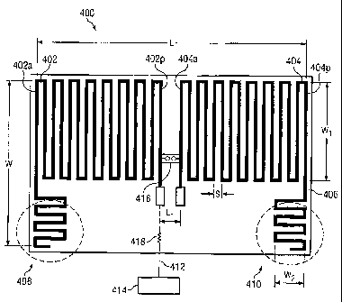
trace line 402 and second antenna trace line 404 and additional cutting of the
edge antenna trace lines
bends 408 and 410 for additional impedance tuning of symmetrical printed
meander dipole antenna 400.
In one embodiment, symmetrical printed meander dipole antenna 400 may further
include a resistor
418 for providing additional frequency bandwidth.
[0043] In one embodiment, first antenna trace line 402 and second antenna
trace line 404 may each
include 16 vertical traces, 402a-402p and 404a-404p, respectively. Vertical
traces 402a-402p and 404a-
404p may have a length L equal to approximately 70 mm, for example. Vertical
traces 402a-402p and
CA 02699166 2010-03-12
WO 2009/034462 PCT/IB2008/002383
404a-404p may have a width W1 equal to approximately 33 mm, for example.
Additionally, the distance
L1 between first antenna trace line 402 and second antenna trace line 404 may
be approximately 5 mm.
The width W of the first antenna trace line 402 and additional trace line
bends 408 is approximately 54
mm, as is the width W of the second antenna trace line 404 and additional
trace line bends 410, in one
example. Preferably, the width W2 of the additional trace line bends 408 and
410 is approximately 6
mm. Further, in one aspect, the distance S between each of the vertical traces
402a-402p and 404a-404p
is approximately 1 mm. In one aspect, vertical traces 402a-402p and 404a-404p
may be made from a
conducting material, such as copper.
[0044] Referring to FIG. 5, a symmetrical printed meander dipole antenna 500
is shown with a first
antenna trace line 502 and a second antenna trace line 504 that are printed on
PCB 506. First antenna
trace line 502 and second antenna trace line 504 may be connected to a control
module 514 via a
connector 512. First antenna trace line 502 and second antenna trace line 504
are printed on one side of
PCB 506. Symmetrical printed meander dipole antenna 500 may further include an
inductor 516
disposed between first antenna trace line 502 and second antenna trace line
504 and additional cutting of
the edge antenna trace lines bends 508 and 510 for additional impedance tuning
of symmetrical printed
meander dipole antenna 500. In one embodiment,. symmetrical printed meander
dipole antenna 500
may further include a resistor 518 for providing additional frequency
bandwidth.
[0045] In one embodiment, first antenna trace line 502 and second antenna
trace line 504 may each
include 16 vertical traces, 502a-502p and 504a-504p, respectively. Vertical
traces 502a-502p and 504a-
504p may have a length L equal to approximately 100 mm, for example. Vertical
traces 502a-502p and
504a-504p may have a width W1 equal to approximately 17 mm, for example.
Additionally, the distance
L1 between first antenna trace line 502 and second antenna trace line 504 may
be approximately 6 mm.
The width W of the first antenna trace line 502 and additional trace line
bends 508 is approximately 54
mm, as is the width W of the second antenna trace line 504 and additional
trace line bends 510, in one
example. Preferably, the width W2 of the additional trace line bends 508 and
510 is approximately 6
mm. Further, in one aspect, the distance S between each of the vertical traces
502a-502p and 504a-504p
is approximately 3 mm.
[0046] Referring to FIG. 6, symmetrical printed meander dipole antenna 600 is
shown with a first
antenna trace line 602 and a second antenna trace line 604 that are printed on
PCB 606. First antenna
trace line 602 and second antenna trace line 604 may be connected to a control
module 614 via a
connector 612. First antenna trace line 602 and second antenna trace line 604
are printed on one side of
11
CA 02699166 2010-03-12
WO 2009/034462 PCT/IB2008/002383
PCB 606. Symmetrical printed meander dipole antenna 600 may further include an
inductor 616
disposed between first antenna trace line 602 and second antenna trace line
604 and additional cutting of
the edge antenna trace lines bends 608 and 610 for additional impedance tuning
of symmetrical printed
meander dipole antenna 600. In one embodiment, symmetrical printed meander
dipole antenna 600
may further include a resistor 618 for providing additional frequency
bandwidth.
[00471 In one embodiment, first antenna trace line 602 and second antenna
trace line 604 may each
include 20 vertical traces, 602a-602t and 604a-604t, respectively. Vertical
traces 602a-602t and 604a-604t
may have a length L equal to approximately 120 mm, for example. Vertical
traces 602a-602t and 604a-
604t may have a width W1 equal to approximately 17 mm, for example.
Additionally, the distance L1
between first antenna trace line 602 and second antenna trace line 604 may be
approximately 6 mm.
The width W of the first antenna trace line 602 and additional trace line
bends 608 is approximately 54
mm, as is the width W of the second antenna trace line 604 and additional
trace line bends 610, in one
example. Preferably, the width W2 of the additional trace line bends 608 and
610 is approximately 6
mm. Further, in one aspect, the distance S between each of the vertical traces
602a-602t and 604a-604t
is approximately 3 mm.
[00481 Referring to FIG. 7, symmetrical printed meander dipole antenna 700 is
shown with a first
antenna trace line 702 and a second antenna trace line 704 that are printed on
PCB 706. First antenna
trace line 702 and second antenna trace line 704 may be connected to a contr
ol module 714 via a
connector 712. First antenna trace line 702 is printed on the top of PCB 706
and second antenna trace
line 704 is printed on the back of PCB 706. Symmetrical printed meander dipole
antenna 700 may
further include an inductor 716 disposed between first antenna trace line 702
and second antenna trace
line 704 and additional cutting of the edge antenna trace lines bends 708 and
710 for additional
impedance tuning of symmetrical printed meander dipole antenna 700. In one
embodiment,
symmetrical printed meander dipole antenna 700 may further include a resistor
718 for providing
additional frequency bandwidth.
[00491 In one embodiment, first antenna trace line 702 and second antenna
trace line 704 may each
include 16 vertical traces, 702a-702p and 704a-704p, respectively. Vertical
traces 702a-702p and 704a-
704p may have a length L equal to approximately 70 mm, for example. Vertical
traces 702a-702p and
704a-704p may have a width W1 equal to approximately 33 mm, for example.
Additionally, the distance
L1 between first antenna trace line 702 and second antenna trace line 704 may
be approximately 5 mm.
The width W of the first antenna trace line 702 and additional trace line
bends 708 is approximately 54
12
CA 02699166 2010-03-12
WO 2009/034462 PCT/IB2008/002383
mm, as is the width W of the second antenna trace line 704 and additional
trace line bends 710, in one
example. Preferably, the width W2 of the additional trace line bends 708 and
710 is approximately 6
mm. Further, in one aspect, the distance S between each of the vertical traces
702a-702p and 704a-704p
is approximately 1 mm. Preferably, the distance LS is 24 mm and the width WS
is 12 mm, for example.
100501 In another embodiment, first antenna trace line 702 and second antenna
trace line 704 may each
include 16 vertical traces, 702a-702p and 704a-704p, respectively. Vertical
traces 702a-702p and 704a-
704p may have a length L equal to approximately 70 mm, for example. Vertical
traces 702a-702p and
704a-704p may have a width W1 equal to approximately 10 mm to 35 mm, for
example. Additionally,
the distance L1 between first antenna trace line 702 and second antenna trace
line 704 may be
approximately 4 mm. The width W of the first antenna trace line 702 and
additional trace line bends
708 is approximately 48 mm, as is the width W of the second antenna trace line
404 and additional trace
line bends 710, in one example. Preferably, the width W2 of the additional
trace line bends 708 and 710
is approximately 6 mm. Further, in one aspect, the distance S between each of
the vertical traces 702a-
702p and 704a-704p is approximately 1 mm. Preferably, the distance LS is 25 mm
and the width WS is
11 mm, for example. In one aspect, vertical traces 702a-702p and 704a-704p may
be made from a
conducting material, such as copper. Symmetrical printed meander dipole
antenna 700 may further
include an inductor having a value of approximately equal to 15 nH and a
resistor value equal to
approximately 64 Ohms. Additionally, the main electrical parameters for the
passive antenna part may
include a standing wave ratio ("SWR") (315 MHz) that is equal to 1.2. A gain
may be equal to
approximately -5 dBi to -6 dBi. Also, the cable location effect may be +/-1
dB. In one embodiment,
the antenna amplifier gain may be about 15 dB and a noise figure may be about
1 dB with residual noise
of the active antenna in the anechoic chamber is less than -99 dBm.
[00511 In one embodiment, symmetrical printed meander dipole antennas 600 and
700 further include a
ground spot that may be located on the bottom side of PCB 606 and 706,
respectively, that may be used
as a ground for the amplifier circuit when using symmetrical printed meander
dipole antennas 600 and
700 in an active receiving embodiment. In one aspect, the lengths and number
of bends of first antenna
trace line 402, second antenna trace line 404, first antenna trace line 502,
second antenna trace line 504,
first antenna trace line 602, second antenna trace line 604, first antenna
trace line 702, and second
antenna trace line 704 may be chosen using electromagnetic software, such as
IE3D, to provide a
desirable resistance, such as 50 Ohms input impedance for a particular
application. Additionally,
impedance tuning may further be optimized by using inductors 416, 516, 616,
and 716 in addition to the
13
CA 02699166 2010-03-12
WO 2009/034462 PCT/IB2008/002383
additional cutting of the trace lines as described herein. In one embodiment
control modules 414, 514,
614, and 714 are RKE control modules.
[00521 PCBs 406, 506, 606, and 706 may be a width that is desirable for a
particular application. The
width of the printed antenna trace lines may be any desired width for a
particular application. In one
embodiment, the width of the printed antenna trace lines 402, 404, 502, 504,
602, 604, 702, and 704 are
approximately 1 mm. As can be seen in FIGS. 4-6, the symmetrical dipole
geometries have an
increasing length among FIGS. 4-6, but all lengths are preferably less than 1
/10 of the wavelength of the
transmitted or received radio frequency RF signal. PCBs 406, 506, 606, and 706
may further include a
ground plane (not shown) with a dielectric board (not shown) disposed thereon.
In one embodiment,
the dielectric board of PCBs 406, 506, 606, and 706 may be composed of FR-4
material and have a
thickness of approximately 1.6 mm and a relative permittivity of 4.4. It
should be understood in the art
that the configuration of the outputs of PCBs 406, 506, 606, and 706 may have
alternative
configurations and the dielectric board may be composed of another material
and have a different
thickness and provide an operable antenna solution. In one embodiment, ground
pads are used as the
second "arm" on each of these symmetrical printed meander dipole antennas 400,
500, 600, and 700; the
pads serve concomitantly as low-noise amplifier grounds. The low-noise
amplifier located at the .
antenna trace line side may increase the sensitivity of the receiver, for
example.
[00531 As further understood in the art, physical parameters of an antenna may
be used for adjusting
bandwidth to receive signals, such as RF signals, over a frequency band for
tuning impedance of the
antenna over the frequency band, and for adjusting gain over the bandwidth.
For example, connectors
412, 512, 612, and 712 are used to conduct RF signals to RF circuits, such as
those associated with
control modules 414, 514, 614, and 714. If the output of the antenna portion
has a certain impedance
that includes only resistive component (reactive component value is equal to),
then if the RF circuit has
the same input impedance, a voltage standing wave ratio ("VSWR") will have a
value of 1.0 and the RF
signal will be completely input into the RF circuit (i.e., no part of the RF
signal will reflect back from the
RF circuit). If the output impedance of symmetrical printed meander dipole
antennas 400, 500, 600, and
700 and the input impedance of the RF circuit do not match, the VSWR increases
to a multiple of 1.0,
where the higher the ratio, the higher the VSWR and the lower the input of the
RF input impedance of
the RF circuit. These fundamental RF principles drive the configuration of
symmetrical printed
meander dipole antennas 400, 500, 600, and 700. Because slight differences in
the configuration of the
symmetrical printed meander dipole antennas 400, 500, 600, and 700 can have
large effects in tuning
symmetrical printed meander dipole antennas 400, 500, 600, and 700 over the
frequency range of a
14
CA 02699166 2010-03-12
WO 2009/034462 PCT/IB2008/002383
desired application(s), many configurations of the basic structure of
symmetrical printed meander dipole
antennas 300, 400, 500, 600, and 700 may be used to provide RF output to
control modules 414, 514,
614, and 714 at a certain resistance (e.g., 50 Ohms) to match a resistance of
an RF circuit (e.g., 50
Ohms). Of course, in practice, it is difficult to have a resistance of an
antenna over a frequency range at
approximately 50 Ohms as, typically, the resistance, even if well tuned, may
be 50 +/_ 10 Ohms, for
example, that varies over the frequency range. In addition, the resistance has
a mathematical imaginary
component that also varies over the frequency of symmetrical printed meander
dipole antennas 300,
400, 500, 600, and 700. These fundamental RF principles can be seen on a Smith
chart (see, for
example, FIGS. 16,19, and 22). As the impedance of the symmetrical printed
meander dipole antennas
300, 400, 500, 600, and 700 and RF circuit vary over the frequency bands, the
matching of the
impedances vary and, therefore, VSWR over the RF bands varies. As the VSWR
varies, the gain of the
system varies because the closer to unity of the VSWR, the higher the gain of
the RF signals being
received by the RF circuit.
[0054] The radiation efficiency 0 for symmetrical printed meander dipole
antennas 300, 400, 500, 600,
and 700 are described below in Table 1. The efficiency and the directionality
were each calculated with
IE3D electromagnetic software both with and without an RF cable. The
simulation results are for these
symmetrical printed meander dipole antennas 300, 400, 500, 600, and 700 with
different linear antenna
sizes are presented graphically in Table 1, below.
CA 02699166 2010-03-12
WO 2009/034462 PCT/IB2008/002383
TABLE 1
Simulation Results of the Radiation Efficiency q for Different Linear Antenna
Sizes
Efficiency n
Type Length (mm) Without Cable With 1 m Cable
Printed Meandered Dipole 70 0.23 0.28
(FIG. 4)
Printed Meandered Dipole 100 0.42 0.45
(FIG. 5)
Printed Meandered Dipole 120 0.52 0.54
(FIG. 6)
Printed Meandered Dipole 70 + ground 0.21 0.33
(FIG. 7) spot
Printed Asymmetrical 70 0.12 0.45
Meander Line (FIG. 1)
Wire Half-Wave Dipole 475 0.98 0.98
[0055] The frequency of the above results in Table 1 is 315 MHz. As can be
seen in Table 1,
asymmetrical meander antenna 50 without a RF cable had the lowest antenna
efficiency value: 0.12 (-
9.2dB). In comparison, symmetrical printed meander dipole antenna 400 was 1.9
times more efficient.
Table 1 also shows that asymmetrical meander antenna 50 with a RF cable had
the same efficiency as
symmetrical printed meander dipole antenna 500 without an RF cable. This
indicates that the RF cable
is a significant enhancement to asymmetrical meander antenna 50. Such an
antenna could therefore be
effective in vehicle applications where electronic components near the RF
cable do not radiate
interference at the 315 MHz frequency band. It is significant to contrast
these findings with those
pertaining to symmetrical printed meander dipole antennas 400, 500, 600, and
700. In the latter
instance, there is scarcely any difference between the efficiency of the
antenna either with or without the
RF cable. This means that the RF cable effect for symmetrical printed meander
dipole antennas 400,
500, 600, and 700 is minimal. Additionally, the ground spot shown in
symmetrical printed meander
dipole antenna 700 does not appear to significantly influence the efficiency
of the dipole.
16
CA 02699166 2010-03-12
WO 2009/034462 PCT/IB2008/002383
[0056] Referring to FIGS. 8-11, polar plots 800-1100 show simulated and
measured results for
symmetrical printed meander dipole antenna 400 and asymmetrical meander
antenna 50. Polar plots
800-1100 show calculated horizontally polarized directionalities with two
different lengths of RF cable,
LC. Antenna orientation with regard to the directionality angles is seen where
the performances of
asymmetrical meander antenna 50 are similar to the performance of symmetrical
printed meander dipole
antenna 400 with total length values that cause a multi-lobe structure (i.e.,
more than one wavelength).
[0057] Polar plot 800 shows the simulated results for symmetrical printed
meander dipole antenna 400
with a RF cable length of 65cm and polar plot 900 shows the simulated results
for symmetrical printed
meander dipole antenna 400 with a RF cable length of 160 cm. Polar plot 800
shows a far field
directivity plot 802 versus angle resulting from a simulation of symmetrical
printed meander dipole
antenna 400 and polar plot 900 shows a far field directivity plot 902
resulting from a simulation of
symmetrical printed meander dipole antenna 400.
[0058] Polar plot 1000 shows the simulated results for asymmetrical meander
antenna 50 with a RF
cable length of 65 cm and polar plot 1100 shows the simulated results for
asymmetrical meander
antenna 50 with a RF cable length of 160 cm. Polar plot 100 shows a far field
directivity plot 1002
versus angle resulting from a simulation of asymmetrical meander antenna 50
and polar plot 1100 shows
a far field directivity plot 1102 resulting from a simulation of asymmetrical
meander antenna 50.
[0059] Referring to FIG. 12, a graph 1200 shows the calculated ratio between
the efficiency q and the
cable length (expressed in cm) for asymmetrical meander antenna 50 shown in
FIG. 1. Efficiency
expressed in dB format was normalized to the half-wave dipole efficiency. As
can be seen, asymmetrical
meander antenna 50 with a RF cable length of approximately 25 cm has an
efficiency almost equivalent
to that of the half wave dipole. In such a configuration, asymmetrical meander
antenna 50 together with
its cable shows more gain than the symmetrical printed meander dipole antenna
400, for example. This
efficiency is also very similar to that of a coaxial antenna with an inner
conductor length value equal to
one quarter of the wavelength. Here, instead of the inner conductor of the
coaxial antenna, a meander
line with a linear size much less than one-quarter wavelength is used, but
with a total trace length of
more than a quarter wavelength.
[0060] Additionally, a mean square error parameter e, averaged over 360 ,
which numerically estimates
the similarity between two power directionality curves: the first when F(O)
corresponds to the antenna
without a cable, and the second when F, (0) corresponds to the antenna with an
RF cable. The results
are presented graphically in Table 2, below.
17
CA 02699166 2010-03-12
WO 2009/034462 PCT/IB2008/002383
[0061]
TABLE 2
Calculated Results
Mean Square
Type Length (mm) Error e
Printed Meandered Dipole (FIG. 4) 70 0.3
Printed Meandered Dipole (FIG. 5) 100 0.16
Printed Meandered Dipole 120 0.15
(FIG. 6)
Printed Meandered Dipole (FIG. 7) 70 + ground spot 0.74
Printed Asymmetrical Meander Line 70 0.81
(FIG. 1)
[0062] As can be seen, asymmetrical meander antenna 50 of FIG. 1 has a maximum
error value s,
which means that this antenna benefits from the largest increase in gain due
to the added effect of the
RF cable, but can suffer from interference effects due to the parasitic
interference sources in a vehicle
located close to the RF cable route. Symmetrical printed meander dipole
antenna 600 has the smallest
error e, which means that this antenna has a minimal benefit from the addition
of the cable, but also
minimal possible interference effects. From these results, it is possible to
conclude that, if a vehicle does
not have electronic components that radiate parasitic emissions at 315 MHz, it
is preferable to use an
asymmetrical design, such as asymmetrical meander antenna 50, with careful RF
cable routing that can
increase the communication range. Nevertheless, if electronic components
radiate parasitic emissions
near the cable path route, a symmetrical dipole antenna, such as symmetrical
printed meander dipole
antennas 400-700 is a better antenna for RKE automotive applications.
[0063] These results were confirmed by actual measurement as well. A passive
meander line dipole
antenna printed on an FR-4 dielectric substrate was placed horizontally (the
substrate board plane was
parallel to the floor plane) on a turntable. The antenna was made to operate
in the transmitting mode.
A horizontally polarized receiving Yagi antenna operating in a frequency range
from symmetrical printed
meander dipole antenna 300 to 1000 MHz was located in the far zone of the
antenna assembly (this
represented a passive antenna under test with a RF cable). Resulting
directionality measurements are
18
CA 02699166 2010-03-12
WO 2009/034462 PCT/IB2008/002383
presented over 360 in the horizontal plane for the horizontal polarization. A
RF cable (RG 174 cable)
was used for the measurements, with losses equal to 0.5 dB per meter in the
315 MHz frequency band.
[00641 The measurement results for symmetrical printed meander dipole antenna
400 and asymmetrical
meander antenna 50 are presented in polar plots 800-1100 and FIGS. 13 and 14.
FIG. 13 is a polar plot
1300 of the measured results for symmetrical printed meander dipole antenna
400 without a RF cable as
shown by a far field directivity plot 1302 and a a far field directivity plot
for a reference antenna 1304.
FIG. 14 is a polar plot of the measured results for asymmetrical meander
antenna 50. All the plots in
FIGS. 8-11 demonstrate the horizontal polarization directionality graphs in
the azimuth plane for an
antenna assembly consisting of a meander line antenna with different RF cable
lengths.
[0065] FIG. 8 shows the directionality of a symmetrical dipole in the case
where the cable length is
equal to 65 cm and FIG. 9 corresponds to a cable length of 1.6 m, as discussed
above. FIGS. 10 and 11
show the horizontally polarized directionality plots in the azimuth plane for
an antenna assembly
consisting of an asymmetrical meander line antenna with an RF cable. FIGS. 10
and 11 show more than
two main lobes. Again, good agreement between the simulated and measured
results are shown in that
both show very strong improvements on the antenna performances because of the
effects of the cable.
[0066] Referring to FIGS. 13 and 14, these plots show the antenna
directionality of symmetrical printed
meander dipole antenna 400 and asymmetrical meander antenna 50 without an RF
cable (the dashed line
indicates the reference antenna directionality). The average (over 360 ) gain
of the printed dipole is less
than the gain of the reference antenna by a value of -4 dB. The average gain
of asymmetrical meander
antenna 50 is less than the gain of the reference antenna by a value of -9 dB.
These measurement results
confirm the findings of the numerical simulation: that the cable effect is not
very significant in regards to
the performance of the symmetrical antenna, such as symmetrical printed
meander dipole antennas 400-
700. As can be seen, the medium (L=100 mm) and large antenna (L=120 mm) sizes
show the same
level of agreement between simulation and measurement results.
[0067] Resistors 418, 518, 618, and 718 maybe used in symmetrical printed
meander dipole antennas
400, 500, 600, and 700, respectively, to increase the range of frequency
bandwidth as described above.
Referring to FIG. 15, a graph 1500 shows a symmetrical printed meander dipole
antenna with resistance
equal to 0 Ohms. As can be seen from graph 1500, the measurement of the
frequency bandwidth is
approximately 9 MHz, beginning at 311.25 MHz and ending at 320.4167 MHz.
Referring to FIG. 16, a
Smith chart 1600 is shown that is used for displaying an exemplary impedance
plot 1618 for a
symmetrical printed meander dipole antenna. In designing a RKE signal path,
for example, a network
19
CA 02699166 2010-03-12
WO 2009/034462 PCT/IB2008/002383
analyzer that is capable of generating the Smith chart 1600 may be used to
analyze impedances over an
RKE frequency range. As shown on the Smith chart 1600, the input impedance
plot 1618 shows input
impedances of a symmetrical printed meander dipole antenna having an impedance
of 50 Ohms.
Because the symmetrical printed meander dipole antenna and RF circuit may be
mismatched in
impedance, a VSWR value is greater than 1 results. A Smith chart has a
normalized impedance plane
1602 defining an inductive impedance (positive imaginary parts) 1606 above the
normalized impedance
plane 1602 and a capacitive impedances (negative imaginary parts) 1604 below
the normalized
impedance plane 1602. In Smith chart 1600, a marker 1608 shows an impedance or
resistance of 28.30
Ohms at 315 MHz. A marker 1610 shows an impedance of 30.92 Ohms at 311.250 MHz
and a marker
1612 shows an impedance of 31.15 Ohms at 320.417 MHz. As understood in the
art, if the input
impedance of the symmetrical printed meander dipole antenna were to match the
RF circuit impedance
at 50 Ohms at 315 MHz, the input impedance plot 1618 would cross at or near 50
Ohms at marker 1608
with little imaginary component. Referring to FIG. 17, a log plot 1700 is
shown corresponding to the
data of FIGS. 15 and 16.
[00681 Referring to FIG. 18, a graph 1800 shows a symmetrical printed mea nder
dipole antenna with
resistance equal to 100 Ohms. As can be seen from graph 1800, the measurement
of the frequency
bandwidth is approximately 16 MHz, beginning at 304.8333 MHz and ending at
320.4167 MHz. This is
a substantial improvement over the frequency bandwidth with a symmetrical
printed meander dipole
antenna having zero resistance value as noted in FIG. 15. Referring to FIG.
19, a Smith chart 1900 is
shown that is used for displaying an exemplary impedance plot 1902 for a
symmetrical printed meander
dipole antenna having a resistance of 100 Ohms. In Smith chart 1900, a marker
1904 shows an
impedance or resistance of 40.65 Ohms at 315 MHz. A marker 1906 shows an
impedance of 30.94
Ohms at 304.8333 MHz and a marker 1908 shows an impedance of 30.94 Ohms at
320.417 MHz.
Referring to FIG. 20, a log plot 2000 is shown corresponding to the data of
FIGS. 18 and 19.
[00691 Referring to FIG. 21, a graph 2100 shows a symmetrical printed meander
dipole antenna with
resistance equal to 68 Ohms. As can be seen from graph 2100, the measurement
of the frequency
bandwidth is approximately 20 MHz, beginning at 300.8333 MHz and ending at
320.8333 MHz. This is
a substantial improvement over the frequency bandwidth with a symmetrical
printed meander dipole
antenna having zero resistance value and 16 MHz as noted in FIGS. 15 and 16,
respectively. Referring
to FIG. 22, a Smith chart 2200 is shown that is used for displaying an
exemplary impedance plot 2202
for a symmetrical printed meander dipole antenna having a resistance of 68
Ohms. In Smith chart 2200,
a marker 2204 shows an impedance or resistance of 46.75 Ohms at 315 MHz. A
marker 2206 shows an
CA 02699166 2010-03-12
WO 2009/034462 PCT/IB2008/002383
impedance of 146.1 Ohms at 30.833 MHz and a marker 2208 shows an impedance of
31.73 Ohms at
320.833 MHz. Referring to FIG. 23, a log plot 2300 is shown corresponding to
the data of FIGS. 21
and 22.
[00701 The previous detailed description is of a small number of embodiments
for implementing the
invention and is not intended to be limiting in scope. One of skill in this
art will immediately envisage
the methods and variations used to implement this invention in other areas
than those described in
detail. The following claims set forth a number of the embodiments of the
invention disclosed with
greater particularity.
21