Note: Descriptions are shown in the official language in which they were submitted.
, CA 02699552 2012-09-13
1
DESCRIPTION
ANTENNA SHEET, TRANSPONDER, AND BOOKLET
[0001]
The present invention relates to an antenna sheet, a transponder, and a
booklet.
BACKGROUND ART
[0002]
There are conventionally known technologies for arranging a wire-wound
antenna coil on a substrate and connecting it to an IC module to form a non-
contact type
communication unit which performs data communications with an external
reading/writing device (e.g. see Patent Document 1).
[0003]
In recent years, systems using non-contact IC card and non-contact IC tags are
being used with the aim of enhancing security. To apply the excellent
characteristics of
such non-contact IC cards, IC tags, and the like in a booklet, such as a
passport and a
savings passbook, it is proposed to form a non-contact type information medium
by
pinching an IC inlet, with an antenna that is connected to a non-contact IC
module,
between outer-cover base materials, and mounting the medium on the booklet by
bonding it to a front cover or the like thereof
Since such a booklet enables electronic data to be entered to the IC inlet and
CA 02699552 2010-03-11
2
printed, enhanced security characteristics and the like can be achieved.
[0004)
Patent Document 2 describes one example of a booklet such as that described
. above. In this booklet, a non-contact type information medium is bonded to
an inner
face of a back cover of the booklet, The non-contact type information medium
is
configured such that, on a top-face side of a first base-material sheet, a
second
base-material sheet having an opening of a predetermined width is affixed to
form a
recess, an IC chip and an antenna coil attached thereto are provided in this
recess, and
an adhesive layer is provided on a bottom-face side of the first base-material
sheet.
Patent Document 1: Japanese Patent No, 3721520
Patent Document 2: Japanese Patent Application, First Publication No.
2002-42068,
DISCLOSURE OF THE INVENTION
Problems to be Solved by the Invention
[0005)
However, in the conventional technology described above, when the portion
where the IC module and the wire-wound antenna coil are connected is subjected
to
repeated flexing, since the wire-wound antenna has an extremely narrow
diameter of,
for example, approximately 0.05 mm to 0,2 mm, there is a problem that the wire-
wound
antenna coil is liable to break after striking the edge of the terminal
section of the IC
module,
Furthermore, when using ultrasound welding and the like to connect the
wire-wound antenna coil to the terminal section of the IC module, there is a
problem of
constriction in the connection sections of the wire-wound antenna coil, making
it liable
CA 02699552 2010-03-11
3
to break.
[0006]
Furthermore, during a manufacturing process, it is necessary to wire each
individual wire-wound antenna onto the substrate, making it difficult to
increase
productivity,
[0007]
Furthermore, many booklets such as that described above are conventionally
formed using paper and the like. Since chloride ions, water, and the like can
easily
permeate through paper, permeation of such substances sometimes leads to
deterioration
of the antenna and the like of the bonded non-contact type information medium,
As a
result, there is an adverse affect on the durability of the non-contact type
infonnation
medium, leading to problems such as a possibility of a decline in the
performance of the
non-contact type information medium while the booklet is being used.
[0008]Furtheimore, in conventional technology, since the IC module is fixed on
the
substrate, when a product in which the substrate and the IC module are covered
with
paper and the like is manufactured, there is a problem that the product
becomes thicker.
In this case, due to the flexibility of paper, there is a problem that the
region where the
IC module is installed expands and contacts other components, breaking the IC
module
and the like.
[0009]
The present invention has been realized in view of these circumstances, and
aims to provide an antenna sheet, a transponder, and a booklet that, when a
product is
manufactured by using a flexible base material such as paper to pinch an IC
module,
enables the product to be made thin.
CA 02699552 2010-03-11
4
Means for Solving the Problem
[0010]
To solve the problems described above, an antenna sheet of the present
-
invention includes a flexible substrate, and an antenna coil that is connected
to a
terminal section of an external IC module including an IC chip and is arranged
on the
substrate; a storing section that stores at least a part of the IC module
being formed on
the substrate.
When connecting the terminal section of the IC chip to a connection section of
the antenna sheet, at least a part of the IC module can be stored in the
storing section.
Consequently, when securing the IC module to the substrate, the thickness of
at least a
part of the IC module is absorbed by the storing section, enabling the product
(e.g. an
inlet) to be made thin.
[0011]
The antenna coil of the antenna sheet of the present invention is formed in a
film shape, the width of the connection section of the antenna coil to be
connected to the
terminal section is larger than the width of the antenna coil, and a pair of
the connection
sections are arranged opposing each other at portions pinching the storing
section in the
substrate.With this configuration, when the IC module terminal section and the
antenna
coil connection section is subjected to repeated flexing, and a stress acts on
the antenna
coil, since the antenna coil is formed in a film shape, in comparison with a
conventional
wire-wound antenna coil, flexibility is enhanced, and concentration of stress
can be
prevented. Moreover, since the width of the connection section to be connected
to the
terminal section of the IC module is increased, stress can be dispersed in the
width
CA 02699552 2010-03-11
direction and prevented from concentrating. In addition, since the antenna
coil is 5
formed on the substrate, the substrate functions as a reinforcing member for
the antenna
coil. This can prevent the antenna coil from striking the edge of the terminal
section of
the IC module. Therefore, breakage of the antenna coil can be prevented,
When connecting the connection sections to the terminal section, since the
connection section of the antenna coil, which is film-shaped and has an
increased width,
is connected to the terminal section of the IC module, constriction is
unlikely to occur
during connecting as it does when using a conventional wire-wound antenna
coil.
Therefore, breakage of the connection sections can be prevented.
Furthermore, when the substrate is plasticized and flows due to heat, since
the
antenna coil is formed in a film shape, in comparison with a conventional wire-
wound
antenna, the contact area of the antenna coil with the substrate increases,
and the flow
resistance of the antenna coil can be increased. Therefore, it is possible to
prevent the
antenna coil from moving according to the flow of the substrate, and to
improve the
reliability of data communication.
Furthermore, since the film-shaped antenna coil can be manufactured
collectively by, for example, etching and the like, in comparison with a
manufacturing
process in which wire-wound antenna coils are individually wired, productivity
can be
noticeably increased,
[0012}
The antenna sheet of the present invention includes a chloride ion-resistant
layer formed such as to cover the antenna coil.
With this configuration, since the chloride ion-resistant layer is formed such
as
to cover the antenna coil, even if incorporated in a booklet made of paper and
such like,
the antenna coil is not damaged by chloride ions that permeate the paper,
CA 02699552 2010-03-11
6
[0013]
The antenna sheet of the present invention includes a water-resistant layer
formed such as to cover the antenna coil.
With this configuration, since the water-resistant layer is formed such as to
cover the antenna coil, even if incorporated in a booklet made from paper and
such like,
the antenna coil is not damaged by chloride ions that permeate the paper.
[0014]
Furthermore, in the antenna sheet of the present invention, the widths of the
connection sections are smaller or similar to the width of the terminal
section.
With this configuration, the connection sections can be connected to the
terminal section along the entire width in the width direction. This enables
the
connection sections to be more reliably connected to the terminal section, and
increases
the reliability of the antenna coil.
[00151
Furthermore, in the antenna sheet of the present invention, the tenninal
section
and the connection sections are connected such as to overlap in a direction
linking the
opposing connection sections, and the length of the connection sections is
larger than
the length of a region where they overlap with the terminal section.
With this configuration, in connecting the connection sections and the
terminal
section, when they are connected such as to overlap in the direction linking
the opposing
connection sections, the edge of the terminal section is further to the inside
than the
edge sides of the length direction of the connection sections. Consequently,
the edge
of the terminal section contacts the connection sections, whose width is
larger than the
antenna coil, Therefore, when the portion where the terminal section of the IC
module
connects to the connection sections of the antenna coil is subjected to
repeated flexing,
CA 02699552 2010-03-11
7
the edge of the terminal section can be received by the connection sections
with
increased widths. This can prevent concentration of stress, and can prevent
breakage
of the antenna coil.
[0016]
Furthermore, in the antenna sheet of the present invention, slit holes are
provided in the substrate and in the connection sections.
With this configuration, if flexing and the like is applied and cracks occur
in the
width direction of the connection sections, when the cracks reach the slit
holes, there is
communication between the cracks traveling in the width direction and the slit
holes
extending in the length direction, stopping the progression of the cracks in
the width
direction. Therefore, the cracks can be prevented from crossing the slit holes
and
progressing in the width direction, and breakage of the antenna coil can be
prevented.
10017]
Furthermore, in the antenna sheet of the present invention, a through hole
that
penetrates the substrate is formed in a region of the substrate where the
antenna coil is
not fonned.
With this configuration, when bonding base materials to both sides of the
antenna sheet, the base materials can be joined together via the through hole.
The
through hole can also increase the flexibility of the antenna sheet, make the
antenna
sheet lighter, and reduce the quantity of base material used.
[0018]
Furthermore, in the antenna sheet of the present invention, the connection
sections of the antenna sheet are welded to the terminal section of the IC
module at a
plurality of points.
CA 02699552 2010-03-11
8
With this configuration, when connecting the terminal section of the IC module
to the connection section of the antenna sheet, a plurality of points can be
alloyed or
thermally fused, and thereby fixed. In comparison with when they are fixed at
only
one point, the connection strength of the terminal section of the IC module
and the
connection section of the antenna sheet with respect to flexing can be
increased.
[0019]
A transponder of the present invention includes an antenna sheet including a
flexible substrate and an antenna coil that is connected to a terminal section
of an
external IC module including an IC chip and is arranged on the substrate, a
storing
section that stores at least a part of the IC module being formed on the
substrate, and an
IC module including an IC chip and a terminal section; the IC module is fixed
to the
antenna sheet, and the antenna sheet is connected to the terminal section of
the IC
module.
With this configuration, the antenna sheet including the transponder can
prevent breakage of the antenna coil, increasing the reliability of data
communication,
and further increasing productivity.
Therefore, according to the transponder of the present invention, it is
possible
to provide an inlet that enables breakage of the antenna coil to be prevented,
has high
data communications reliability, and high productivity.
[0020]
Furthermore, the transponder of the present invention includes a pair of base
materials that pinch the antenna sheet and the IC module,
With this configuration, the antenna sheet including the transponder can
prevent breakage of the antenna coil, increase the reliability of data
commnnication, and
further increase productivity. The base materials can also reinforce the
connection
CA 02699552 2010-03-11
points between the connection sections of the antenna sheet and the terminal
section of 9
the IC module.
Therefore, according to the present invention, it is possible to provide a
transponder that can prevent breakage of the antenna coil, and that has high
reliability of
data communication and high productivity.
[0021]
Furthermore, in the transponder of the present invention, a base material
opening for storing at least a part of the IC module is provided in at least
one of the pair
of base materials.
With this configuration, the thickness of the section of the IC module that is
stored in the base material opening is absorbed by the base material, enabling
the
transponder to be made thin.
[0022]
Furthermore, in the transponder of the present invention, a through hole is
formed in the antenna sheet, and the pair of base materials are joined via the
through
hole.
With this configuration, the base materials can be joined together via the
through hole of the antenna sheet. This increases the strength of the joint
between the
transponder and the base materials, and can prevent peeling of the base
materials from
the antenna sheet.
[0023]
Furthermore, in the transponder of the present invention, a cover material is
joined to a face of at least one of the pair of base materials.
With this configuration, the external appearance and textme of the transponder
can be altered to suit its purpose, enabling it to be applied in various
fields. Also, sinee
_ n
CA 02699552 2010-03-11
10
the transponder includes the antenna sheet, it becomes possible to provide a
transponder
which can prevent breakage of the antenna coil, and which achieves highly
reliable data
communication and high productivity,
[0024]
Furthermore, in the transponder of the present invention, the pair of base
materials are porous or have a fibrous structure.
With this configuration, since the thickness of the antenna sheet can be
absorbed by the base materials which are porous or have a fibrous structure, a
flatter
transponder can be manufactured.
[0025]
When the transponder of the present invention is applied in a data carrier
with
non-contact type IC such as, for example, a card-shaped commuter pass with IC
or an
electronic money card, the antenna sheet including the inlet can prevent
breakage of the
antenna coil of the data carrier with non-contact type IC, thereby increasing
the
reliability of data communication and increasing productivity,
[0026]
When the transponder of the present invention is applied in an inlay for a
booklet or a book cover, such as, for example, a booklet-shaped identification
certificate
such as a passport or a pass book, the antenna sheet including the inlay can
prevent
breakage of the antenna coil of the data carrier with non-contact type IC,
thereby
increasing the reliability of data communication and increasing productivity,
[0027]
A problem of using a conventional substrate made from a thermoplastic
material with a low softening point such as PET-G is that, when manufacturing
a
product by thermal lamination of the substrate, the wire-wound antenna fixed
on the
CA 02699552 2010-03-11
substrate moves in accordance with softening and flow of the substrate due to
heat, 11
affecting the data communication characteristics and reducing the reliability.
In contrast, since the substrate of the antenna sheet described above is
formed
from polyethylene naphthalate or polyethylene terephthalate, whereby the
heat-resistance temperature of the substrate can be increased in comparison
with that of
conventionally used thermoplastic materials with a low softening point such as
PET-G.
Consequently, when, for example, manufacturing a product by thermal lamination
of a
substrate, even if the substrate is subjected to heat, it can be prevented
from plasticizing
and flowing. Therefore, the antenna coil can be prevented from moving in
accordance
with the flow of the substrate, and reliability of data communication can be
increased.
[0028] A booklet of the present invention includes an antenna sheet
including a
flexible substrate, and an antenna coil that is connected to a terminal
section of an
external IC module including an IC chip and is arranged on the substrate, a
storing
section that stores at least a part of the IC module being formed on the
substrate, an IC
module including an IC chip and a terminal section, and a pair of base
materials that
pinch the antenna sheet and the IC module; the IC module being fixed to the
antenna
sheet, and the antenna sheet being connected to the terminal section of the IC
module.
Effect of the Invention
[0029]
According to the present invention, when using a flexible base material such
as
paper to pinch an IC module and manufacture a product, it is possible to
provide an
antenna sheet, a transponder, and a booklet that can make the product thin,
CA 02699552 2010-03-11
12
BRIEF DESCRIPTION OF THE DRAWINGS
[0030]
FIG. lA is a plan view of an antenna sheet according to a first embodiment of
the present invention.
FIG. 1B is a bottom view of an antenna sheet according to a first embodiment
of the present invention.
FIG. 2A is a cross-sectional view of a connection section of a jumper wire and
an antenna circuit of the antenna sheet according to the first embodiment of
the present
invention.
FIG. 2B is a cross-sectional view of a connection section of a jumper wire and
an antenna circuit of the antenna sheet according to the first embodiment of
the present
invention.
FIG. 3A is a plan view of an IC module according to the first embodiment of
the present invention,FIG. 3B is a cross-sectional view taken along the line
A¨A' in a plan view of an
IC module according to the first embodiment of the present invention,
FIG. 4A is an enlarged plan view of an inlet according to the first embodiment
of the present invention.
FIG. 4B is a cross-sectional view taken along the line B¨B' in an enlarged
plan
view of an inlet according to the first embodiment of the present invention.
FIG. 5A is an explanatory cross-sectional view of a manufacturing method of
an inlet according to the first embodiment of the present invention.
FIG. 5B is an explanatory cross-sectional view of a manufacturing method of
an inlet according to the first embodiment of the present invention.
MG. 6 is an enlarged plan view of an antenna sheet and an inlet according to a
CA 02699552 2010-03-11
13
second embodiment of the present invention.
FIG 7A is a plan view of an antenna sheet and an inlet according to a third
embodiment of the present invention.
FIG. 7B is a plan view of an antenna sheet and an inlet according to the third
embodiment of the present invention.
FIG 7C is a plan view of an antenna sheet and an inlet according to the third
embodiment of the present invention.
FIG. 8A is a plan view of an inlay according to an embodiment of the present
invention.
FIG. 8B is a front view of an inlay according to the embodiment of the present
invention,
FIG, 9A is an explanatory plan view of a manufacturing method of an antenna
sheet according to the embodiment of the present invention.
PIG. 9B is an explanatory plan view of a manufacturing method of an IC
module according to the embodiment of the present invention.
FIG. 10 is an explanatory plan view of a manufacturing method of an inlay
according to the embodiment of the present invention.
FIG 11 is a perspective view of a schematic configuration of an electronic
passport according to the embodiment of the present invention,
FIG. 12 is a plan view of a deformation example of an antenna sheet according
to the embodiment of the present invention.
FIG. 13 is a view showing a booklet which a non-contact type infonmation
medium according to a fourth embodiment of the present invention is attached
to.
FIG. 14 is a view showing.a mold of an IC inlet of the same non-contact type
information medium.
CA 02699552 2010-03-11
FIG. 15 is a cross-sectional view of the same non-contact type information
14
medium attached to the same booklet 101.
FIG. 16 is a view showing a cut state of the same IC inlet when manufacturing
the same non-contact type information medium.
FIG. 17 is a view showing dimensions of each part of the same non-contact
type information medium in an example.
FIG. 18A is a view showing an IC inlet a modification of a non-contact type
information medium of the present invention. I8B is a view showing an IC inlet
a modification of a non-contact type
information medium of the present invention.
Reference Symbols
[0031)
1, 1A, 1B, IC, 11)
Antenna sheet I
2
Substrate
4 Antenna coil
7 Opening
8, 9 Antenna connecting
lands (Connection sections)
12, 13, Reinforcing patterns
(reinforcing sections)
=
18 Slit holes
19B, 19C, 19D Through holes
20 IC module
22 IC chip
25 Antenna land (terminal
section)
30 Inlet
CA 02699552 2010-03-11
40 Inlay 15
41, 42 Base materials
100 Electronic passport (inlay with cover, data carrier
with non-contact
type IC)
101, 101A Booklet 101
110, 110A Non-contact type information medium
112 Sheet
112A Through hole
113 Antenna coil
114 IC chip
115 Porous base materials
116 Adhesive (chloride ion-resistant layer)
Wl, W2, W3, W4 Width
L, L3, L4 Length
BEST MODE FOR CARRYING OUT THE INVENTION
10032)
<First Embodiment>
the drawings.Subsequently, a first embodiment of the invention will be
explained based on
(Antenna Sheet)
FIG lA is a plan view of an antenna sheet 1 according to this embodiment, and
FIG 1B is a bottom view. As shown in FIG IA, the antenna sheet 1 includes a
flexible
substrate 2 formed from, for example, polyethylene naphthalate (PEN) or
polyethylene
terephthalate (PET). The thickness of the substrate 2 is selected as
appropriate within
CA 02699552 2010-03-11
16
a range of, for example, approximately 0.02 mm to approximately 0.10 mm. An
antenna circuit 3 is formed on a surface of the substrate 2.
[00331
The antenna circuit 3 is made by performing etching and the like to pattern an
aluminum thin film formed on the surface of the substrate 2, and is formed in
a thin-film
shape having a thickness of approximately 0.02 mm to 0,05 mm.
The antenna circuit 3 includes an antenna coil 4 formed in a roughly
rectangular spiral shape that corresponds to the shape of the substrate 2. An
inside end
of the antenna coil 4 expands in volume in a roughly circular shape, forming a
terminal
section 5. Bent portions (rectangle corners) of the antenna coil 4 are formed
in roughly
circular arc shapes.
[0034)
An outside end 6 of the antenna coil 4 is led toward one corner of the
substrate
2. A roughly rectangular opening 7 is formed slightly to the antenna coil 4
side of one
corner of the substrate 2, The opening 7 can store a part of an IC module
explained
later. While a storing section that can store a part of the IC module is here
described as
being the opening 7, this is not limitative of the invention. For example,
instead of
providing an opening in the substrate 2, a recess can be provided as a storing
section,
with part of the IC module being accommodated in this recess, In comparison to
using a
recess, an opening obtains a deeper storing section with more space for
storing the IC
module, and can therefore increase the planarity of the antenna sheet 1.
The outside end 6 of the antenna coil 4 that is led toward one corner of the
substrate 2 is led toward one side 7a of the opening 7, and is connected to an
antenna
connecting land 8 (connecting section) which is formed along the side 7a. The
antenna
connecting land 8 is a roughly rectangular terminal section fOnned by
increasing the
CA 02699552 2010-03-11
17
width W1 of the antenna coil 4.
[0035]
An antenna connecting land 9 (connecting section) is formed on one side 7b
opposing the side 7a of the opening 7 where the antenna connecting land 8 is
formed.
. A wire 10 is one part of the antenna coil 4, and is connected to the antenna
connecting
land 9 formed opposing the antenna connecting land 8. In a manner similar to
the
opposing antenna connecting land 8, the antenna connecting land 9 is formed in
a
roughly rectangular shape along the side 7b of the opening 7 by increasing the
width
W2 of the wire 10. One end of the wire 10 connects to the antenna connecting
land 9,
and another end side increases in volume in a roughly circular shape to form a
terminal
section 11.
(0036)
As shown in FIG. 1B, reinforcing patterns 12 and 13 (reinforcing sections)
that
reinforce the antenna connecting lands 8 and 9 are formed on a face on an
opposite side
to the face where the antenna circuit 3 is formed, in correspondence with the
formation
regions of the antenna connecting lands 8 and 9. The reinforcing patterns 12
and 13
are formed in rectangular shapes corresponding to the shapes of the antenna
connecting
lands 8 and 9 along the outlines of the antenna connecting lands 8 and 9 when
viewed
from above by, for example, etching and the like of a metal thin film as used
for the
antenna circuit 3, or by a similar method.
[0037]
By thus forming the reinforcing patterns 12 and 13 in correspondence with the
formation regions of the connection section 8 on the face of an opposite side
to the face
where the antenna circuit 3 including the antenna connecting land 8 of the
substrate 2 is
formed, the connection section 8 can be supported by both the substrate 2 and
the
CA 02699552 2010-03-11
18
reinforcing patterns 12 and 13 formed on the rear side thereof, whereby the
connection
section 8 can be reinforced, This increases the flexural strength of the
connection
section 8, and can prevent breakage of the antenna coil 4 even when the
section where a
terminal section 25 of an IC module 20 and the connection section 8 of the
antenna coil
4 are connected is subjected to repeated flexing.
[0038]
A jumper wire 14 is formed on a face on the opposite side to the face where
the
antenna circuit 3 of the substrate 2 is formed, and connects the terminal
section 5 of the
antenna coil 4 to the terminal section 11. The jumper wire 14 is formed using,
for
example, a similar method to that used for the antenna circuit 3. Both ends of
the
jumper wire 14 are increased in volume in a roughly circular shape to form
terminal
sections 15 and 16. The terminal sections 15 and 16 of the jumper wire 14 are
provided in correspondence with the formation regions of the terminal section
5 and the
terminal section 11 of the antenna coil 4 respectively. The terminal sections
15 and 16
of the jumper wire 14 and the terminal sections 5 and 11 of the antenna coil 4
are
electrically connected together in conductive sections 17, which are formed in
a
plurality of point-like shapes in the formation regions of the terminal
sections 15 and 16,
[0039]
As shown in PIG. 2A3 the conduction section 17 is for example formed by a
crimping process of applying pressure to the terminal section 15 (terminal
section 16) of
the jumper wire 14 and the terminal section 5 (terminal section 11) of the
antenna coil 4
such as to pinch them from both sides, thereby breaking the substrate 2 and
achieving
physical contact between the terminal sections 5 and 15 (11 and 16).
The conduction section 17 can be formed using a method other than the
connection by the crimping process described above; as shown in PIG, 2)3, for
example,
CA 02699552 2010-03-11
19
it is acceptable to form a through hole 19A that penetrates the formation
regions of the
terminal sections 5 and 15 (11 and 16), fill the through hole 19A with a
conductive paste
19 such as silver paste, and electrically connect the terminal section 15
(terminal section
= 16) of the jumper wire 14 to the terminal section 5 (terminal section 11)
of the antenna
coil 4.
[0040]
(IC Module)
Subsequently, an IC module 20 connected to the antenna circuit 3 of the
antenna sheet 1 will be explained.
FIG. 3A is a plan view of an IC module 20 according to this embodiment, and
FIG. 3B is a cross-sectional view taken along the line A¨A' of FIG. 3A.
As shown in FIGS. 3A and 3B, the IC module 20 is formed from a lead frame
21, an IC chip 22 mounted on the lead frame 21, and a sealing resin section 23
that seals
the IC chip 22,
[0041] =
The lead frame 21 is formed roughly in the shape of a rectangle with its
comers
rounded to circular arc shapes when viewed from above. The lead frame 21 is
formed
from, for example, a copper-thread metal film and the like made by weaving
copper
thread into a film and silver plating this film.
The lead frame 21 includes a die pad 24 that securely supports the IC chip 22,
and an antenna land 25 (terminal section) that is connected to an input/output
pad of the
IC chip 22.
[0042]
The die pad 24 is slightly larger than the outer shape of the IC chip 22, and
is
fixed to the bottom of the IC chip 22. A gap S is provided between the die pad
24 and
CA 02699552 2010-03-11
the antenna land 25, electrically insulating them from each other.
20
The antenna land 25 is connected to the input/output pad of the IC chip 22 by
bonding wires 26 of, for example, gold (Au). Since the antenna land 25 is used
as a
terminal section of the IC module 20 that is connected to an external circuit,
it is formed
extending along the long direction (length L direction) of the IC module 20.
[0043)
The sealing resin section 23 is formed roughly in the shape of a square with
its
corners rounded to circular arc shapes when viewed from above. The sealing
resin
section 23 is formed from, for example, a resin material such as epoxy resin,
and covers
the IC chip 22, the input/output pad of the IC chip 22, the bonding wires 26,
the
connection section between the antenna land 25 and the bonding wires 26, etc.
The
sealing resin section 23 is filled into the gap S between the die pad 24 and
the antenna
land 25, and extends across both of them. Here, the thickness Ti of the IC
module 20
is, for example, approximately 0.3 ram.
[0044)
(Inlet (also termed Transponder))
As shown in FIGS. 4A and 4B, by electrically connecting the antenna land 25
of the IC module 20 to the antenna connecting lands 8 and 9 of the antenna
sheet 1, and
thereby securing the IC module 20 to the antenna sheet 1, there is formed an
inlet 30
that includes the antenna sheet 1 and the IC module 20.
Here, the opening 7 of the antenna sheet 1 is opened in a roughly square shape
= corresponding to the sealing resin section 23, and slightly larger than the
outer shape of
the sealing resin section 23, enabling the opening 7 to store the roughly
square-shaped
sealing resin section 23 of the IC module 20.
[0045]
CA 02699552 2010-03-11
= 21
The width W3 of the pair of antenna connecting lands 8 and 9 provided
opposing each other on both sides of the opening 7 of the antenna sheet 1 is
roughly the
same as, or slightly smaller than, the width W4 of the antenna land 25 of the
IC module
20.
The length L3 of the antenna connecting lands 8 and 9 of the antenna sheet I
is
larger than the length L4 of overlapping sections of the antenna land 25 of
the IC
module 20 and the antenna connecting lands 8 and 9. In this embodiment, the
length
. L3 of the antenna connecting lands 8 and 9 is roughly twice the length L4 of
the
overlapping sections of the antenna land 25 and the antenna connecting lands 8
and 9.
[0046]
Subsequently, an operation of this embodiment will be explained.
When the inlet 30 shown in FIGS. 4A and 4B is subjected to repeated flexing,
this applies a stress to the section where the antenna land 25 of the IC
module 20 is
connected to the antenna connecting lands 8 and 9 of the antenna sheet 1. At
this time,
since the antenna coil 4 is formed by patterning of an aluminum thin film on
the
substrate 2, its flexibility is superior to that of a conventional antenna
coil formed by
winding a wire, and stress is prevented from concentrating in specific points.
Forming the antenna coil 4 from aluminum in this manner can achieve a lower
cost than when using another metal, such as copper, to form the antenna coil
4.
Furthermore, when joining the antenna connecting land 8 of the antenna coil 4
and the
antenna land 25 of the IC module 20, optimizing the joining conditions enables
them to
be alloyed or thermally fused, and firmly joined together.
[0047]
The width W3 of the antenna connecting lands 8 and 9 of the antenna coil 4
connected to the antenna land 25 of the IC module 20 is made larger than the
widths W1
CA 02699552 2010-03-11
22
and W2 of the antenna coil 4, so that it is roughly the same as, or slightly
smaller than,
the width W4 of the antenna land 25. This can disperse the stress in the width
W3
direction, and prevent it from concentrating. Furthermore, the antenna
connecting
lands 8 and 9 can be connected along the entire width of the antenna land 25
in the
width W4 direction, and the antenna connecting lands 8 and 9 can be reliably
connected
to the antenna land 25, enhancing the reliability of the antenna coil 4 and
the inlet 30.
[0048]
The length L3 of the antenna connecting lands 8 and 9 of the antenna sheet 1
is
made larger than the length L4 of the overlapping sections between the antenna
land 25
of the IC module 20 and the antenna connecting lands 8 and 9. Furthermore, in
this
embodiment, the length L3 of the antenna connecting lands 8 and 9 is roughly
twice as
long as the length L4 of the overlapping sections between the antenna land 25
and the
antenna connecting lands 8 and 9. As a result, edges 25e of the antenna land
25 are
connected such as to be positioned roughly at the center of the insides of the
ends of the
antenna connecting lands 8 and 9 on the antenna coil 4 side. The edges 25e of
the
antenna land 25 consequently contact roughly with the centers of the antenna
connecting
lands 8 and 9 whose width W3 is made larger than the widths W1 and W2 of the
antenna coil 4.
[0049]Therefore, when the sections where the antenna land 25 of the IC module
20 is
connected to the antenna connecting lands 8 and 9 of the antenna coil 4 are
subjected to
repeated flexing, the edges 25e of the antenna land 25 can be received roughly
in the
centers of the antenna connecting lands 8 and 9 whose width W3 is made larger.
This
can prevent concentration of stress in the antenna coil 4, and can thereby
prevent
breakage of the antenna coil 4.
CA 02699552 2010-03-11
[0050] 23
In addition, since the antenna coil 4 and the antenna connecting lands 8 and 9
are formed on the substrate 2, the substrate 2 functions as a reinforcing
material for
them. This prevents the antenna coil 4 with small widths WI and W2 from making
contact with the edges 25e of the antenna land 25, and can prevent breakage of
the
antenna coil 4.
[0051]
Reinforcing patterns 12 and 13 that reinforce the antenna connecting lands 8
and 9 are formed on a face of the substrate 2 that is on the opposite side to
the face
where the antenna circuit 3, in correspondence with the formation regions of
the antenna
connecting lands 8 and 9, The antenna connecting lands 8 and 9 are thus
supported by
both the substrate 2 and the reinforcing patterns 12 and 13 on its rear face,
whereby the
antenna connecting lands 8 and 9 can be reinforced.
[0052]Therefore, the flexural strength of the antenna connecting lands 8 and 9
is
increased, and, when the sections where the antenna land 25 of the IC module
20 is
connected to the antenna connecting lands= 8 and 9 of the antenna coil 4 are
subjected to
repeated flexing, breakage of the antenna connecting lands 8 and 9, and
breakage of the
antenna coil 4, can be prevented.
[0053]
Even if the substrate 2 breaks due to stress, for example, the reinforcing
patterns 12 and 13 can be made to contact the antenna connecting lands 8 and
9,
whereby they can assist the antenna connecting lands 8 and 9, and prevent the
antenna
coil 4 from breaking.
[0054]
CA 02699552 2010-03-11
Furthermore, since the thin-film antenna coil 4 of this embodiment can be 24
manufactured collectively by, for example, etching and the like, in comparison
with a
manufacturing process in which wire-wound antenna coils are individually
wired,
productivity of the antenna sheet I can be noticeably increased.
[0055]
(Inlet Manufacturing Method)
Subsequently, a method of manufacturing the inlet 30 by connecting the
antenna connecting lands 8 and 9 of the antenna sheet 1 to the antenna land 25
of the IC
module 20 will be explained.
When connecting the antenna connecting lands 8 and 9 of the antenna sheet 1
to the antenna land 25 of the IC module 20, as shown in FIGS. 4A and 4B, the
sealing
resin section 23 of the IC module 20 is stored in the opening 7 of the antenna
sheet 1,
and the antenna land 25 is connected to the antenna connecting lands 8 and 9
in such a
manner that they face each other.
[0056]
The connection between the antenna land 25 and the antenna connecting lands
8 and 9 is accomplished by, for example, resistance welding or laser welding.
As
shown in FIG 5A, in resistance welding, a pair of welding electrodes 31 and 32
are
separated and made to contact in the width W4 direction of the antenna land 25
of the
IC module 20. A pressure of approximately 5N/rnm2 to 70N/mna2, and preferably
approximately 40N/mm2, is then applied from welding electrodes 31 and 32
between the
antenna land 25 and the antenna connecting land 8. That is, a pressure of
approximately 2.51\l/mm2 to 35N/mm2, and preferably approximately 20N/mm2, is
applied from each of the welding electrodes 31 and 32, The coupling can be
made
more reliable by welding at multiple spots.
CA 02699552 2010-03-11
[0057] 25
While the above pressure is being applied, a welding current I is fed from one
welding electrode 31 to the other welding electrode 32. A voltage is applied
between
the welding electrodes 31 and 32 for a time of approximately 0.5 ms to 10.0
ms, such
that the welding current I becomes, for example, approximately 300A to 600A.
Consequently, current I supplied from the welding electrode 31 enters the
antenna
connecting land 8 from the antenna land 25, and enters the antenna land 25
from the
antenna connecting land 8 at the point where the other welding electrode 32
.makes
contact. At this time, heat is generated at the interface between the antenna
land 25
and the antenna connecting land 8 in the section where the welding electrodes
31 and 32
make contact.
[0058]
Due to the heat generated at this interface, the antenna land 25 and the
antenna
connecting land 8 are welded and alloyed or thermally fused, thereby joining
them
together. Moreover, by reversing the direction ofthe welding cuiTent 1, it is
possible to .
achieve a well-balanced joint between the antenna land 25 and the antenna
connecting
land 8 at the sections where the welding electrodes 31 and 32 made contact.
If the voltage, pressing force, and voltage application time are adjusted in
the
manner described above, the joining conditions can be optimized, enabling the
antenna
land 25 and the antenna connecting land 8 to be alloyed or thermally fused,
and firmly
joined together.
[0059]
When pressure is applied between the antenna land 25 and the antenna
connecting land Sin the manner described above, the contact resistance of the
antenna
land 25 and the antenna connecting land 8 decreases. This weakens the
resistant
CA 02699552 2010-03-11
26
heating, and reduces in the welding energy of the antenna connecting land 8,
which is
made from aluminum having lower welding temperature than the antenna land 25.
Scattering of the antenna connecting land 8 during welding can thereby be
prevented,
and a stable joint can be obtained.
[0060]
Subsequently, the antenna connecting land 9 and the antenna land 25 are joined
by welding, according to the same procedure as that of joining the antenna
connecting
land 8 and the antenna land 25.
Thus, it is possible to manufacture an inlet 30 wherein the antenna land 25 of
the IC module 20 and the antenna connecting lands 8 and 9 of the antenna sheet
1 are
welded at two points in the width W4 direction.
[0061]
As shown in FIG. 513, in resistance welding, it is possible to arrange the
pair of
welding electrodes 31 and 32 in a separated manner in the length L direction
of the IC
module 20, make one of the welding electrodes 31 contact the antenna
connecting land
8, and make the other welding electrode 32 contact on a point on the antenna
land 25
where the antenna land 25 and the antenna connecting land 8 are joined, In
this case,
the antenna land 25 and the antenna connecting land 8 are pressured by
applying a
pressure of approximately 5N/mm2 to 70N/num2, preferably approximately
40N/mm2, to
the welding electrode 32 provided on the antenna land 25.
[0062]
Subsequently, while the above pressure is being applied, a welding current I
is
fed from one welding electrode 31 to the other welding electrode 32. The
current,
voltage, and application time of the welding current I are the same as in the
resistance
welding described in FIG SA. At this time, the current I supplied from the
welding
CA 02699552 2010-03-11
electrode 31 enters from the antenna connecting land 8, and enters the antenna
land 25 27
from the antenna connecting land 8 at the point where the other welding
electrode 32
makes contact. At this time, heat is generated at the interface between the
antenna land
25 and the antenna connecting land 8 in the section where the other welding
electrode
32 makes contact, whereby they are welded and alloyed or thermally fused, and
joined.
[0063]
If the pressure at the time of welding the antenna connecting land 8 is
relatively
high in comparison with the antenna land 25, the contact resistance of the
welded
section on the antenna connecting land 8 side becomes relatively low.
Consequently,
the resistance heating of the welded section on the antenna connecting land 8
side can
be relatively reduced in comparison with that on the antenna land 25, and the
resistance
heating welding energy on the antenna connecting land 8 side can be reduced.
This
can prevent the antenna connecting land 8, which has a welding temperature
that is
relatively low in comparison with the antenna land 25, from scattering during
welding,
and can achieve a stable joint, whereby the joining reliability and data
carrier reliability
can be increased.
[0064]
The welding electrodes 31 and 32 are then moved in the directions of the
widths W3 and W4 of the antenna connecting land 8 and the antenna land 25, and
a
similar procedure is employed to join them by welding at a plurality of points
in the
directions of their widths W3 and W4.
Using a similar procedure as that when joining the antenna connecting land 8
and the antenna land 25, the antenna connecting land 9 and the antenna land 25
are then
joined by welding them at a plurality of points in the directions of their
widths W3 and
W4.
CA 02699552 2010-03-11
28
Thus it is possible to manufacture the inlet 30 wherein the antenna land 25 of
the IC module 20 and the antenna connecting lands 8 and 9 of the antenna sheet
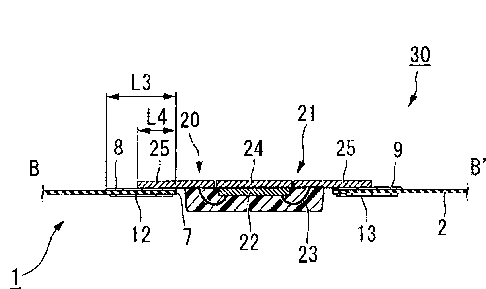
1 are
joined by welding at a plurality of points in the directions of the widths W3
and W4.
[0065] =
As described above, when securing the IC module 20 to the substrate 2, the
opening 7 that can store the sealing resin section 23 of the IC module 20 is
formed in the
antenna sheet 1, whereby the thickness of the sealing resin section 23 of the
IC module
20 is absorbed into the opening 7 of the substrate 2, enabling the inlet 30 to
be made
thinner.
[0066]
Furthermore, by arranging the pair of welding electrodes 31 and 32 in
separation on the antenna land 25 in the directions of the widths W3 and W4
direction,
and welding the antenna land 25 to the antenna connecting lands 8 and 9 by
resistance
welding, a larger joining area can be achieved than when joining a
conventional
wire-wound antenna coil using ultrasound welding and the like.
Also, by arranging the pair of welding electrodes 31 and 32 in separation in
the
length L direction of the IC module 20, only the other welding electrode 32
need be
positioned on the antenna land 25, This enables the antenna land 25 to be made
smaller.
[0067]
When connecting the antenna land 25 to the antenna connecting lands 8 and 9,
by welding them at a plurality of points in the width W3 and width W4
directions and
joining them together, the antenna land 25 and the antenna connecting lands 8
and 9 can
be fixed at a plurality of points, This can increase joining strength between
the antenna
land 25 of the IC module 20 and the antenna connecting lands 8 and 9 of the
antenna
CA 02699552 2010-03-11
sheet 1 with respect to flexing. 29
[0068]
When welding the antenna land 25 and the antenna connecting lands 8 and 9,
since the antenna connecting lands 8 and 9 which are filmy and have an
increased width
W3 are welded to the antenna land 25, there is no constriction during
connecting as
there is in a conventional wire-wound antenna coil. Therefore, breakage of the
antenna
coil 4 can be prevented.
[0069]
Furthermore, since the length L3 of the antenna connecting lands 8 and 9 is
larger than the length of the antenna land 25 extending in the length L
direction, the
supporting area of the IC module 20 and the substrate 2 that is supported by
the antenna
connecting lands 8 and 9 can be increased. This increases durability against
stress, and
can prevent breakage of the antenna coil 4 even when flexing acts on the
antenna
connecting lands 8 and 9.
[0070]
Furthermore, the reinforcing patterns 12 and 13 are formed in formation
regions of the antenna connecting lands 8 and 9 on a face of the substrate 2
of the
antenna sheet 1 that is on the side opposite to the face where the antenna
connecting
lands 8 and 9 are formed. Consequently, heat during resistance welding can be
transmitted to the reinforcing patterns 12 and 13, and released to the
outside. This can
prevent the substrate 2 from overheating and melting. Therefore, dirt can be
prevented
from sticking to the resistance welding apparatus and the product, and, in
addition,
decrease in the flexural strength of the antenna sheet 1 can be prevented.
[0071]
Furthermore, since the inlet 30 includes the antenna sheet 1 described above,
CA 02699552 2010-03-11
30
breakage of the antenna coil 4 due to the antenna sheet 1 can be prevented,
increasing
the reliability of data communications, and further increasing the
productivity of the
inlet 30. It is therefore possible to provide the inlet 30 that enables
breakage of the
antenna coil 4 to be prevented, has high data communications reliability, and
high
productivity.
[0072]
As described above, according to this embodiment, it is possible to provide
the
antenna sheet 1 that prevents breakage of the antenna coil 4, increases
reliability, and
also increases productivity. Moreover, by including this antenna sheet 1, it
is possible
to provide the inlet 30 that enables breakage of the antenna coil 4 to be
prevented, has
increased reliability, and increased productivity.
[0073]
<Second Embodiment>
Subsequently, referring to FIG lA to FIG. 3B, FIG 4B to 5B, and FIG. 6, a
second embodiment of the present invention will be explained. An antenna sheet
IA
of this embodiment differs from the antenna sheet 1 described in the first
embodiment in
that slit holes 18 are formed in the antenna connecting lands 8 and 9. Since
the other
features are similar to those of the first embodiment, like reference numerals
are
appended to like parts, and these are not repetitiously explained.
[0074)
As shown in FIG. 6, slit holes 18 are provided in the antenna connecting lands
8
and 9 of the antenna sheet 1A, and extend along the length L3 direction of the
antenna
connecting lands 8 and 9. A plurality of the slit holes 18 are formed in the
width W3 -
direction of the antenna connecting lands 8 and 9. The slit holes 18 are
formed such
that, when the antenna connecting lands 8 and 9 are joined to the antenna land
25 of the
CA 02699552 2010-03-11
31
IC module 20, the edges 25e of the antenna land 25 are in the middles of the
slit holes
18.
[0075]
In the antenna sheet JA formed in this manner, if the joint section between
the
antenna connecting lands 8 and 9 and the antenna land 25 is subjected to
flexing and the
like, and cracks occur in the width W direction due to the edges 25e of the
antenna land
25 making contact with the antenna connecting lands 8 and 9, when the cracks
reach the
slit holes 18, there is communication between the cracks traveling in the
width W
direction and the slit holes 18 extending in the length L3 direction, stopping
the
progression of the cracks in the width W direction.
[0076]
Therefore, the cracks can be prevented from crossing the slit holes 13 and
progressing in the width W direction of the antenna connecting lands 8 and 9,
and
breakage of the antenna coil 4 can be prevented.
Furthermore, since a plurality of the slit holes 18 are formed in the width W
direction of the antenna connecting lands 8 and 9, when a crack has progressed
beyond
an outer-side slit hole 18, another slit hole 18 adjacent thereto can prevent
further
progression of that crack.
[0077]
<Third Embodiment>
Subsequently, referring to FIG IA to FIG 513, and FIG 7A to FIG 7C, a third
embodiment of the present invention will be explained. Antenna sheets 113 to
1D of
this embodiment differ from the antenna sheet 1 described in the first
embodiment in
that through holes 19B to 19D are formed in the substrate 2, Since the other
features
are similar to those of the first embodiment, like reference numerals are
appended to
CA 02699552 2010-03-11
32
like parts, and these are not repetitiously explained.
[0078]
As shown in FIG. 7A, in the antenna sheet 1B, a roughly rectangular through
hole 19B is formed in a region of the substrate 2 where the antenna coil 4 is
not formed,
and penetrates the substrate 2. As shown in FIG 7B, in the antenna sheet IC, a
plurality of roughly rectangular through holes 19C are formed in the region of
the
substrate 2 where the antenna coil 4 is not formed, the substrate 2 being
formed in a
lattice shape, As shown in FIG 7C, in the antenna sheet 11), a plurality of
roughly
circular through holes 191) are formed in rows in the region of the substrate
2 where the
antenna coil 4 is not formed.
[0079]
When the through holes 19B to 191) are formed in this manner in the substrates
2 of the antenna sheets 1B to ID, it becomes possible, when bonding base
materials
(explained later) to both sides of the antenna sheets 1B to 1D, to join the
base materials
via the through holes 19B to 19D. This can prevent peeling of the base
materials from
the antenna sheets 1B to 11). The through holes I9B to 191) increase the
flexibility of
the antenna sheets 1B to ID, make them lighter, and enable the quantity of
material used
for the substrate 2 to be reduced.
[0080)
(Inlay)
Subsequently, referring to FIG. 8A and FIG 8B, an inlay 40 including the inlet
described in the above embodiment will be explained.
As shown in FIGS. 8A and 8B, an inlay 40 includes the inlet 30 described in
the above embodiment, and a pair of base materials 41 and 42 that pinch the
inlet 30.
25 The inlay 40 is formed to a desired thickness T2 by pinching the inlet 30
between the
CA 02699552 2010-03-11
33
base materials 41 and 42 and joining them into a single piece by lamination.
[0081]
A porous base material, a base material having a fibrous structure, or the
like, is
used as the base materials 41 and 42. For example, an insulating plastic film
(PET-G:
noncrystalline copolyester, PVC: vinyl chloride resin, etc.), or an insulating
synthetic
sheet (Teslin (Registered trademark), a polyolefm synthetic sheet manufactured
by PPG
Industries), or Yupo {Registered trademark) a polypropylene synthetic sheet
manufactured by Yupo Corporation) is used,
[0082]
Since the inlay 40 includes the inlet 30 including the antenna sheet 1
described
in the first embodiment, the antenna sheet 1 can prevent breakage of the
antenna coil 4,
the reliability of data communication can be increased, and productivity can
be
increased. Furthermore, the base materials 41 and 42 can reinforce the points
of
connection between the antenna connecting lands 8 and 9 of the antenna sheet 1
and the
= antenna land 25 of the IC module 20.
It is therefore possible to provide the inlay 40 wherein breakage of the
antenna
coil 4 is prevented, and which achieves high reliable data communication, and
high
productivity.
[0083]
When the inlet 30 including the antenna sheets 113 to 1D with the through
holes
1913 to 19D, described in the third embodiment, is used in the inlay 40, the
base
materials 41 and 42 can be joined together via the through holes 19B to 19D.
This can increase the joint strength of the inlet 30 to the base materials 41
and
-42, and prevent peeling of the base materials 41 and 42 from the inlet 30.
[0084]
CA 02699552 2010-03-11
34
When the base materials 41 and 42 are forcedly peeled off, due to difference
in
the joint strengths of the section where they were joined together and the
section where
they were joined to the inlet 30, the inlet 30 is broken by the peeling of the
base
materials 41 and 42. This can prevent unauthorized modification of the inlay
40.
By forming the through holes 19B to 19D in the antenna sheet 1, the
flexibility
of the inlay 40 can be increased, the inlay 40 can be made lighter, and the
quantity of
material used for the substrate 2 of the antenna sheet 1 can be reduced.
[0085]
(Method of Manufacturing the Inlay)
Subsequently, a method of manufacturing the inlay 40 will be explained,
Firstly, the inlet 30 is pinched between the pair of base materials 41 and 42,
and
joined to them.
When the synthetic sheets mentioned above are used as the base materials 41
and 42, the inlet 30 is joined to the base materials 41 and 42 using an
adhesive
laminating method of applying an adhesive to the antenna sheet 1, or to the
faces of the
base materials 41 and 42 that contact the antenna sheet 1, and joining them at
a
relatively low temperature of, for example, approximately 70 C to 140 C.
[0086]
As the adhesive, for example, EVA (ethylene vinyl acetate resin)-based, EAA
(ethylene-acrylic acid copolymer resin)-based, polyester-based, polyurethane-
based, and
the like, can be used.
Instead of applying an adhesive coating, an adhesive sheet that uses the resin
used in the adhesives mentioned above can be pinched between the antenna sheet
1 and
the base materials 41 and 42.
[0087]
CA 02699552 2010-03-11
When using the thermoplastic film mentioned above as the base materials 41 35
and 42, the inlet 30 is joined to the base materials 41 and 42 using a thermal
laminating
method of melt-bonding them by applying pressure to them while heating them at
a
temperature that exceeds the softening temperature of the base materials 41
and 42, e.g.
approximately 130 C to l 70`C. To accomplish reliable melt-bonding, the
adhesive
mentioned above can also be used when employing the therrnal laminating
method.
[0088]
After the inlet 30 is joined to the base materials 41 and 42 to form a single
piece, the outer shape of this single piece is shaped as desired.
Thus the inlay 40 shown in FIG. 8A and FIG. 8B can be manufactured.
[0089]
Here, the softening temperature of the base materials 41 and 42 is
approximately 100 C to 150 C for PET -Q and approximately 80 C to 100 C for
PVC.
As described in the first embodiment, the substrate 2 of the antenna sheet 1
is
made from PEN or PET. The softening temperature of PEN is approximately 269 C,
and the softening temperature of PET is approximately 258*C, That is, in
comparison
with a thermoplastic material having a low softening point such as PET-G,
which was
used for substrates in conventional antenna sheets, the heat-resistance
temperature of the
substrate 2 can be increased,
[00901
Accordingly, when the base materials 41 and 42 and the inlet 30 are heated to
approximately 130 C to 170 C, the base materials 41 and 42 soften, whereas the
substrate 2 of the antenna sheet 1 does not. Thus, when the inlet 30 including
the
antenna sheet 1 and the base materials 41 and 42 are laminated and joined by
thermal
lamination, even if heat is applied to the substrate 2 of the antenna sheet 1,
the substrate
CA 02699552 2010-03-11
36
2 can be prevented from plasticizing and flowing, Therefore, the antenna coil
4 can be
prevented from moving in accordance with the flow of the substrate 2, and the
reliability
of data communication can be increased.
[0091]
Even if the substrate 2 is heated in excess of its softening temperature such
that
it is plasticized by the heat and flows, since the antenna coil 4 is formed in
a film shape
as described above, in comparison with a conventional wire-wound antenna coil,
there is
a larger contact area of the antenna coil 4 with the substrate 2, whereby the
flow
resistance of the antenna coil 4 can be increased. Therefore, it is possible
to prevent
the antenna coil 4 from moving according to the flow of the substrate 2, and
to improve
the reliability of data communication,
[0092)
(Method of Mass-producing Antenna Sheet) Inlet, and Inlay)
Subsequently, a method of mass-prodncing the antenna sheet 1, the inlet 30,
and the inlay 40 described above will be explained. The following explanation
centers
on a mass-production method, and will not explain other steps. For steps other
than
the mass-production method, publicly known manufacturing methods can be used.
[0093]
As shown in FIG 9A, aluminum thin films are collectively formed on a
substrate sheet 50 with a plurality of formation regions for antenna sheets 1
arranged
thereon in a matrix. The formed aluminum thin films are then collectively
patterned,
and an antenna circuit 3 is formed in each formation region la. In a similar
manner to
the antenna circuit 3, jumper wires 14 and reinforcing patterns 12 and 13 (see
FIG. 1E)
are collectively formed in each formation region la on the rear face of the
substrate
sheet 50 in relation to the face where the antenna circuit 3 is formed.
CA 02699552 2010-03-11
37
[0094]
Subsequently, terminal sections 5 and terminal sections 11 of the antenna coil
4
of the antenna circuit 3 are collectively connected to terminal sections 15
and 16 of the
jumper wires 14. Openings 7 for storing the sealing resin.sections 23 of the
IC
modules 20 are collectively provided in the formation regions la. The antenna
sheets
1 that were collectively forrned in the plurality of formation regions la on
the substrate
sheet 50 are then cut and separated as individual antenna sheets 1.
Thus a large quantity of the antenna sheets 1 can be collectively mass-
produced,
and productivity of manufacturing the antenna sheets 1 can be increased.
[0095]
The IC module 20 is mass-produced in parallel with the mass-production of the
antenna sheets 1.
As shown in FIG. 9B, lead frames 21 are collectively formed in formation
regions 20a on a metal tape 60 where a plurality of formation regions 20a for
IC
modules 20 are arranged in a matrix. IC chips 22 are then collectively mounted
on die
pads 24 of the lead frames 21 in the formation regions 20a, and input/output
pads of the
IC chips 22 are collectively connected by bonding wires to the antenna lands
25 (see
FIG 3B). Sealing resin sections 23 are formed collectively in each of the
formation
regions. The IC modules 20 collectively formed in the formation regions 20a of
the
metal tape 60 are then cut and separated as individual IC modules 20.
[0096]
= While the sealing resin section 23 of each separated IC module 20 is
stored in
the opening 7 of each separated antenna sheet 1, the antenna sheets 1 and the
IC
modules 20 are joined by resistance welding as described above.
Thus, the inlets 30 can be collectively mass-produced, and their manufacturing
CA 02699552 2010-03-11
38
productivity can be increased.
[0097]
Subsequently, as shown in FIG. 10, a plurality of formation regions 40a for
inlays 40 are provided on a first base-material sheet 71 and on a second base-
material
sheet 72, Inlets 30 are provided in each of the formation regions 40a of the
first
base-material sheet 71. The second base-material sheet 72 is then arranged on
the
inlets 30 such that the formation regions 40a of the first base-material sheet
71 and the
formation regions 40a of the second base-material sheet 72 overlap.
[0098]
As in the method of manufacturing the inlay 40 described above, the
base-material sheets 71 and 72 are joined to the inlet 30 using a joining
method that is
suitable for the material quality of the base-material sheet 71. The inlays 40
formed
collectively in the formation regions 40a are then cut as required, with a
plurality of
inlays 40 linked together or with separated individual inlays 40.
In this manner, the inlays 40 can be collectively mass-produced, and their
manufacturing productivity can be increased.
[0099]
(Electronic Passport)
Subsequently, an electronic passport 100 will be explained as one example of a
data carrier with non-contact type IC.
As shown in FIG. 11, an electronic passport 100 includes the inlay 40
described
above as its front cover. A cover material 43 is joined to one face of the
inlay 40 and
becomes the front cover of the electronic passport 100.
[0100]
When the cover material 43 is joined to the inlay 40 in this manner, the
external
CA 02699552 2010-03-11
appearance and texture of the wire 10 including the inlay 40 can be made
similar to a 39
conventional passport. Also, since the inlay 40 includes the antenna sheet 1
described
above, it is possible to provide the electronic passport 100 wherein breakage
of the
antenna coil 4 can be prevented, and which has high reliability of data
communication
and high productivity.
[0101]
The present invention is not limited to the embodiment described above. For
example, the shape of the antenna coil need not be rectangular. The number of
winds
of the antenna coil 4 is also not limited to the embodiment described above.
With
regard to the material quality of the antenna circuit, it can be made from a
material other
than aluminum, such as, for example, gold, silver, or copper.
Since the terminal section 25 of the IC module 20 is often made from copper,
when the antenna coil 4 is formed from copper, the connection section 8 of the
antenna
coil 4 and the terminal section 25 of the IC module 20 can be formed from the
same
metal, increasing the joint performance between the connection section 8 and
the
terminal section 25.
[0102)
As shown in FIG 12, perforations M can be formed in the antenna sheet 1,
After the inlet has, been pinched between the base materials and joined to
them, when
the base materials are attempted to be peeled from the inlet, stress
concentrates in the
perforations M in the antenna sheet 1, whereby the antenna sheet 1 is cut
along the
perforations M, and the antenna sheet 1 breaks. Therefore, unauthorized
modification
of the data carrier with non-contact type IC can be prevented.
[0103] When using an adhesive material to join the inlet to the
base materials, the
CA 02699552 2010-03-11
40
adhesive can be applied in a predetermined pattern, such that the joint
strength of the
inlet and the base materials is made non-uniform. Consequently, when the base
materials are attempted to be peeled from the inlet, a non-uniform stress acts
on the
antenna sheet, cutting and breaking the antenna sheet. Therefore, unauthorized
modification of the data carrier with non-contact type IC can be prevented.
[0104]
It is possible to form the slit holes, which extend in the length direction of
the
antenna connecting land, in only one point in the width direction, This can
increase
the connection area between the antenna connecting land and the antenna land.
[0105]
The opening in the substrate of the antenna sheet need not be formed.
Furthermore, the position of the opening is not limited to that described in
the
embodiment, For example, the opening can be formed along one side of the
substrate.
The entire IC module can be stored in the opening. The shape of the opening
can be
formed freely in accordance with the shape of the IC module to be stored in
it.
[0106]
Base material openings for storing at least a part of the IC module can be
formed in the base materials that pinch the inlet, at roughly the same
position as the
opening in the antenna sheet. Consequently, when pinching the inlet between
the base
materials, at least a part of the IC module can be stored in the base material
openings,
whereby the thickness of that section can be absorbed by the base materials,
and the
inlay can be made thin.
When the antenna sheet 1 shown in FIG 4B is pinched between a pair of base
materials and made into a product, a storing section (an opening or a recess)
having
roughly the same shape as the antenna land 25 when viewed from above can be
CA 02699552 2010-03-11
41
provided in the base material to be attached to the antenna land 25 side, and
the antenna
land 25 can be stored in this storing section. A storing section (an opening
or a recess)
having roughly the same shape as the sealing resin of the IC chip 22 when
viewed from
above can be provided in the base material to be attached to the opposite side
to the
antenna land 25 side, and the sealing resin of the IC chip 22 can be stored in
this storing
section.
With this configuration, when the antenna sheet 1 is pinched between a pair of
base materials and made into a product, the thickness of the product can be
reduced, and
the antenna sheet 1 can be more reliably fixed by the pair of base materials.
[0107)
The joint section between the antenna connecting land and the antenna land of
the module, which are joined by resistance welding, can be covered with epoxy
resin,
urethane resin, and the like. This can increase the reliability, vibration
resistance,
impact resistance, abrasion resistance, and the like, of the joint section.
[0108]
While the embodiment describes an electronic passport as an example of a data
carrier with non-contact type IC including an inlay, the inlay of the present
invention
can also be used in, for example, electronic identification documents and
various types
of electronically confirmable activity history documents,
[0109]
When the inlet of the present invention is applied in, for example, a card
type
data carrier with non-contact type IC, such as a commuter pass with an IC or
an
electronic money card, the antenna sheet including the inlet can prevent
breakage of the
antenna coil of the commuter pass with an IC, the electronic money card, and
the like,
increasing the reliability of data communication and increasing productivity.
CA 02699552 2010-03-11
42
[0110]
<Fourth Embodiment>
A non-contact type information medium (hereinafter abbreviated as
'information medium') according to a fourth embodiment of the present
invention will
be explained based on the drawings.
FIG 13 is a perspective view of a booklet 101 including an information
medium 110 of this embodiment. The information medium 110 is affixed while
being
pinched between one of two cover members 102, which constitute a front cover
and a
rear cover of the booklet 101, and an inner bonding sheet 103 that is bonded
to that
cover member 102, A plurality of text sheets 104 are bound between the front
cover
and the rear cover, enabling the booklet 101 to be used for various purposes
such as a
savings passbook,
Incidentally, the information medium 110 can be attached to face of one of the
cover members 102 of the booklet 101, In this case, the information medium 110
is
preferably attached to the inner face of the cover member 102 (the face where
the cover
members 102 touches the text sheets 104), rather than to its outer face. This
configuration can protect the information medium 110 from external collisions
against
the booklet 101,
Alternatively, the information medium 110 can be attached to one of the pages
of the text sheets 104 of the booklet 101. For example, a predetermined page
of the
text sheets 104 is given a larger area than the other pages, and folded such
that its area
becomes the same as the other pages, enabling the information medium 110 to be
stored
in a space formed by the folded section. The folded section is sealed by a
method such
as gluing or stitching.
[0111]
CA 02699552 2010-03-11
FIG. 14 is a view showing a mold of an IC inlet 111 that constitutes a part of
the 43
information medium 110. The IC inlet 111 includes an insulating sheet 112, an
antenna coil 113 formed on both sides of the sheet 112, and an IC chip 114
attached to
the sheet 112.
[0112]
Various types of resin, such as polyethylene terephthalate (PET) can suitably
be
used as the material for the sheet 112. The antenna coil 113 is formed by a
method
such as etching, wire bonding, or printing, using a conductor such as aluminum
or silver.
Of these, aluminum is inexpensive, making it preferable when considering the
manufacturing cost. The antenna coil 113 includes an antenna loop 113A
provided On
one face of the antenna coil 113, and a jumper wire 113B provided on another
face.
The end of the jumper wire 11313 is electrically connected to the antenna loop
113A, via
a through hole (not shown) provided in the sheet, or by a method such as
crimping.
[0113] The IC chip 114 is electrically connected to the antenna
coil 113 by welding or
the like, and attached to the sheet 112. This enables the IC inlet 111 to
transmit and
receive data to/from an external data reading device and such like in a non-
contact
manner.
[0114]
FIG 15 is a cross-sectional view of an information medium 110 attached to a
booklet 101. The information medium 110 is formed by using two sheet-like
porous
base materials 115 to pinch an IC inlet 111 from above and below. The IC inlet
111
and the porous base materials 115 are joined in a single piece by an adhesive
116.
[0115] In consideration of a manufacturing step of the information
medium 110
CA 02699552 2010-03-11
described below, the porous base materials 115 should preferably have
thermoplasticity. 44
Specifically, a base material can be obtained using a resin such as
polyethylene,
polypropylene, polyvinyl chloride, polyvinylidene chloride, polystyrene,
polyvinyl
acetate, polyester, or a combination of such resins, which is then subjected
to a process
such as mixing with porous particles such as silica, foaming by the addition
of air during
kneading, and stretching followed by punching. Since this type of base
material is
commercially available as resin sheet and synthetic paper in which print
suitability is
given td an inkjet, an offset, and the like, these can be used.
[0116]
Similarly, the adhesive 116 is preferably hot-melting. Specifically, adhesives
made from various types of thermoplastic resin, such as an ethylene-vinyl
acetate
copolymer (EVA)-based, ethylene-acrylic acid copolymer (EAA)-based, ethylene
methyl acrylic acid copolymer (EMAA)-based, polyester-based, polyamide-based,
polyurethane-based, and olefin-based, can suitably be used.
[0117]
A substance that is resistant to chloride ions is mixed into the adhesive 116,
and
prevents the permeation of chloride ions. That is, the layer that includes the
adhesive
116 also functions as a chloride ion-resistant layer, which covers the antenna
coil 113
formed on the IC inlet 111 and prevents the chloride ions from contacting the
antenna
coil 113, thereby preventing deterioration such as corrosion. Such an adhesive
116 can
easily be obtained by adding an epoxy-based cross-linking agent to an EAA-
based
aqueous emulsion adhesive, or by using a gravure coater to apply an acrylic
emulsion
adhesive and the like according to a predetermined coating thickness, etc.
[0118] To form a chloride ion-resistant layer using the adhesive
116, in addition to the
CA 02699552 2010-03-11
material quality, consideration must also be given to the thickness of the
layer formed 45
by the adhesive 116. Tests were carried out to clarify the relationship
between these.
Methods used in the tests will be explained.
[0119]
(Test Samples)
Using a TESLIN Sheet' (a product manufactured by PPG Industry; thickness =
380 p.m) as porous base materials, an IC inlet having an aluminum antenna coil
was
pinched and affixed onto a sheet made from PET.
As the adhesive, three types of conventional adhesives were used: an
EMAA-based adhesive, an EMAA-based adhesive containing an epoxy-based
cross-linking agent, and an acrylic-based adhesive 116; the coating
thicknesses and
additive quantities were varied. These samples were used in a salt water spray
test
described below.
Samples were also created in which each of the adhesives complying with these
conditions was applied directly to the IC inlet without pinching it between
porous base
materials, and these samples were used in a hydrochloride test described
below.
(Test 1: Salt Water Spray Test)
A salt water spray test was conducted in compliance with IS010373-1, and the
results were evaluated in the following three stages.
A: No corrosion whatsoever, B: Partial corrosion, C: Total corrosion and
defective
performance.
(Test 2: Hydrochloride Test)
A uniquely set testing method, performed according to the following
procedures.
(1) One drop of 2N hydrochloride (11C1) was dropped onto each sample, obtained
by
CA 02699552 2010-03-11
applying each type of adhesive directly to an IC inlet, which was then covered
from 46
above with a film of PET so that it did not dry.
(2) Each sample was then put into an 80 C oven, and the time taken for
the aluminum
to melt was measured.
Table 1 shows results obtained for each sample in Test 1 and Test 2,
[0120]
Table 1
Adhesive
Coating Thickness Test 1
Test 2
EMAA-based thermoplastic adhesive
4 gm C
1 minute
EMAA-based thermoplastic adhesive
8 um C
2 minutes
EMAA-based thermoplastic adhesive
12 um B
4 minutes
EMAA-based thermoplastic adhesive
4 pm B
3 minutes
+ epoxy-based cross-linking agent 1%
EMAA-based thermoplastic adhesive
4 um A
10 minutes
+ epoxy-based cross-linking agent 5%
Acrylic-based thermoplastic adhesive
4 uin B
3 minutes
Acrylic-based thermoplastic adhesive
8 um A
8 minutes
[0121]
As shown in Table 1, the results of Test 1 and Test 2 indicated a consistently
good correlation. The samples that were joined using only an EMAA-based
thermoplastic adhesive in the conventional manner could not obtain sufficient
durability
against the salt water spray, even when the thickness of the adhesive coating
was
increased.
[0122]
CA 02699552 2010-03-11
In contrast, when an epoxy-based cross-linking agent is added to the 47
EMAA-based thermoplastic adhesive, the adhesive becomes resistant to chloride
ions.
Durability was enhanced by increasing the mixture ratio of the epoxy-based
cross-linking agent.
5 Furthermore, the acrylic-based adhesives had
greater durability against salt
water spray than the EMAA-based adhesives, and were resistant to chloride
ions.
Their chloride ion resistance was increased by making the coating thicker.
[0123]
The above results indicate that, by adjusting the mixture ratio of a substance
10 that is resistant to chloride ions, or by selecting an adhesive
made from a material that is
resistant to chloride ions and adjusting its coating thickness, it is possible
to form a
chloride ion-resistant layer having a desired resistance to chloride ions.
= [0124]
A method of manufacturing the information medium 110 configured as
15 described above will be explained.
Firstly, an antenna coil 113 is made by providing an antenna loop 113A and a
jumper wire 11313 on a sheet 112. An IC chip 114 is connected the antenna coil
113 to
form an IC inlet 111. Up to this point, the method is similar to a
conventional method
for manufacturing an IC inlet.
20 [0125]
As shown in FIG. 16, to achieve a good joint between the IC inlet 111 and
porous base materials 115, the periphery of the sheet 112 is cut away; in
addition, a
region of the sheet 112 that is inside the antenna loop 113A is removed,
forming a
through hole 112A which penetrates in the thickness direction of the sheet
112,
CA 02699552 2010-03-11
The through hole 112A can be suitably formed using a punching mold. 48
Therefore, even in cases such as when IC inlets are mass-produced by foaming a
great
many antenna coils on a single large sheet, punching enables a great many
through holes
to be easily made.
[0126]
With regard to achieving a good joint with the porous base materials, the size
of
the through hole 112A is preferably set such that the area of a cross-section
orthogonally
intersecting the thickness direction of the through hole 112A occupies 60% or
more of
the region enclosed within the innermost antenna of the antenna loop 113A.
With
regard to the same point, the area of the sheet 112 is preferably set at not
less than 3%
and less than 20% of the area of the porous base material 115 it is joined to.
[0127]
One face of each of the two porous base materials 115 formed with a desired
size is coated with an adhesive 116 which has been made resistant to chloride
ions in the
manner described above. The faces coated with the adhesive 116 are arranged
opposite the IC inlet 111, which is then pinched and pressed by the porous
base
materials 115 from above and below. In this manner, a chloride ion-resistant
layer
including the adhesive 116 is formed such as to cover the antenna coil 113.
[0128]
When the porous base materials 115 are made from thermoplastic resin, if heat
is applied at the same time as applying pressure, the porous base materials
115 soften
and deform, whereby projections and recesses on the surface of the IC inlet
111 due to
the IC chip 114 and the like are absorbed by the porous base materials 115. As
a result,
an inforination medium 110 having flat top and bottom faces can be obtained.
CA 02699552 2010-03-11
49
A conventional method of manufacturing an IC card and the like can be used in
the above process, which can be executed using, for example, a hot press.
[01291
As shown in FIG. 15, the information medium 110 thus obtained is pinched
between the front cover member 102 and the inner bonding sheet 103, and, when
these
are all joined in a single piece using an adhesive (not shown), the booklet
101 including
the information medium 110 can be obtained.
The porous base materials 115 that constitute the outer faces of the
information
medium 110 have good close attachment to various types of adhesive, and can
therefore
be excellently joined without problems, even when using a water-based emulsion
adhesive and the like used in conventional booklet joining. Furthermore, since
the
outer faces of the information medium 110 are flatly formed without
projections and
recesses, the information medium 110 can be attached without spoiling the
external
appearance of the booklet 101.
[0130]
When joining the cover members 102 to the information medium 110, it is
preferable to use a reaction curing type adhesive with no volume change. When
a dry
curing type adhesive with volume change is used, if a part of the information
medium
includes projections and recesses, the quantity of adhesive used will increase
in the
recesses. As a result, there is greater volume reduction when drying, and
there are
cases where the external appearance is spoiled due to a partial collapse of
cover
members 102 and the like which overlap the recesses.
As the adhesive with no volume change, it is possible to use, for example, a
two-part mixed type epoxy-based adhesive, a moisture curing type silicon-based
adhesive, a one-part curing type urethane-based adhesive, and the like.
Various types
CA 02699552 2010-03-11
50
of hot-melt adhesive can also be used, such as EVA-based, EAA-based, polyester-
based,
polyamide-based, polyurethane-based, and olefin-based. Of these adhesives,
from the
viewpoints of workability and durability, a reactive type hot-melt adhesive is
more
preferable.
[0131]
Using examples, the information medium 110 and the booklet 101 of this
embodiment will be further explained.
(Examples)
1. Creating an IC inlet
A PET sheet having a thickness of 38 micrometers (gm) was used as the sheet
112. Aluminum deposition and printing of a mask layer having the same shape as
the
antenna coil 113 were performed on both faces of the sheet 112, and pattern
etching was
used to form an antenna loop 113A on one face and a jtunper wire 113B on the
other
face. In addition, the antenna loop 113A and the jumper wire 11313 were joined
by
caulking, and an IC chip 114 was welded to the connection terminal section of
the
antenna coil 113.
FIG. 17 shows dimensions of each section of an information medium 110A in
this test. The outer periphery of the roughly square antenna loop 113A is 80
millimeters (mm) x 48 mm, and its inner periphery is 67 mm x 37 mm.
Subsequently, a part of the sheet 112 that is inside the antenna loop 113A was
punched away to form a through hole 112A having a roughly square shape of 65
ruin
35 nun. Moreover, leaving an outline that is 2 mm fiom the outer periphery of
the
antenna loop 113A and the IC chip 114, the sheet 112 that was further to the
outside
than that was removed by punching. The cross-sectional area orthogonal to the
thickness direction of the through hole 112A thereby becomes approximately 91%
of
CA 02699552 2010-03-11
51
the region inside the periphery of the antenna loop 113A. In this manner thc
IC inlet
111 was produced.
[0132]
2, Preparing the Porous Base Materials
A Teslin sheet (a product manufactured by PPG Industries; thickness; 380 tan)
was used as the material for the porous base materials 115, An adhesive,
obtained by
mixing 1 part by weight of a soluble epoxy curing agent with 20 parts by
weight of an
EMAA-based aqueous emulsion adhesive (AC-3100, a product manufactured by Chuo
Rika Kogyo Corporation), was applied to one face of each sheet at an amount of
5g/m2
(coating thickness: approximately 5 inn). After drying, two sheets of 150 mm
200
mm were cut, obtaining porous base materials 115. At this point in time, the
area of
the IC inlet 111 was 15% of the area of the porous base materials 115,
A hole corresponding in size to the lead frame of the IC chip 114 was then
drilled into one of the porous base materials 115, and a hole corresponding in
size to the
mold of the IC chip 114 was drilled into the other porous base material 115.
[0133]
3, Manufacturing the Information Medium
The IC inlet 111 and the porous base materials 115 were arranged such that the
read frame and mold of the IC chip 114 were stored in the holes formed in the
respective porous base materials 115. The IC inlet 111 was then laminated by
pinching it from above and below by the porous base materials 115, and
temporarily
held by spot heating.
The porous base materials 115 and the IC inlet 111 that were temporarily held
by spot heating were pinched between two stainless steel plates and subjected
to heating
and pressurizing to join them completely together, thereby obtaining the
information
CA 02699552 2010-03-11
52
medium 110A. The heating and pressurizing conditions were adjusted as
appropriate
between a heater unit temperature of 100C to 160 C, pressure of 5 KgF/cm2 to
30
KgF/cm2, and a processing time of 15 seconds to 120 seconds.
[0134]
4. Attachment to the Booklet
A cloth for book cover (Enviromate 1-1, a product manufactured by ICG
Holliston) was used as the material for the cover members 102. This was cut to
the
same size as the information medium 110A to obtain the cover members 102.
A moisture curing hot-melt adhesive (Esdain 9635, a product manufactured by
Sekisui Fuller Corp.) was melted with a heat roll coater, and an amount of 20
g/m2 was
applied to the cover members. The outer faces of the porous base materials 115
of the
information medium 110A were affixed to the cover members 102 coated with the
hot-melt adhesive, pressurized with rollers, and thereafter subjected to an
aging process.
Subsequently, a plurality of text sheets 104 and one inner bonding sheet 103
are
collated, and their centers are stitched using a sewing machine, thereby
manufacturing a
text section with the inner bonding sheet 103 attached to an outermost
section. A
water-based emulsion adhesive (SP-2850, a product manufactured by Konishi
Corp.)
was then applied at an amount of 20g/m2 to the porous base materials 115 on
the
opposite side of the information medium 110A to the side affixed to the cover
members
102, and the porous base materials 115 were affixed to the inner bonding sheet
103,
The book thus obtained is opened and cut to 125 mm x 180 mm, obtaining a
booklet
101. That is, the dimensions of the porous base materials 115 shown in FIG. 17
are the
dimensions when the booklet 101A is folded.
(Comparative Example)
CA 02699552 2010-03-11
53
In a comparative example, although the IC inlet 111 was made using the same
method as in the example, the size of the through hole 112A was 40 nun x 30
nun.
The cross-sectional area orthogonal to the thickness direction of the through
hole 112A
was approximately 48% of the region inside the periphery of the antenna loop
113A,
Moreover, the IC inlet 111 was attached to a booklet using the same procedure
as the example, to obtain a booklet having roughly the same external
appearance.
[0135]
The front and rear covers of the booklet 101A of the example manufactured in
the manner described above are formed smoothly, DO projections or recesses
being
generated by the attachment of the information medium 110A. Furthermore, in
various
durability evaluation experiments, including storing it in a high temperature
and high
moisture environment and subjecting it to a bend test, the IC inlet 111
suffered no
deterioration, especially of the antenna coil 113, and thus achieved excellent
results.
[0136]
When attempting to remove only the IC inlet from the booklet of the
comparative example, in the booklet of the comparative example, it was
possible to
separate the IC inlet from the porous base materials and remove it without
breaking the
antenna coil. On the other hand, in the booklet 101A of the example, when
attempting
to peeling away the porous base materials 115, since the porous base materials
115 are
directly and firmly joined together at the through hole 112A with a large area
and
around the IC inlet 111, a part of the antenna coil 113 and the porous base
materials 115
was broken, and the IC inlet 111 could not be removed in a usable state.
[0137]
According to the information medium 110 of this embodiment, when the IC
inlet 111 is pinched between the porous base materials 115, which have been
coated
CA 02699552 2012-09-13
54
with the chloride ion-resistant adhesive 116, and joined to them in a single
piece, a
chloride ion-resistant layer is formed such as to cover the antenna coil 113
including the
antenna loop 113A and the jumper wire 113B. Therefore, even when the
information
medium 110 is attached to a booklet, chloride ions that permeate the cover
members 102
and the inner bonding sheet 103 are prevented from reaching the antenna coil
113 and
acting upon it, whereby deterioration of the antenna coil 113 is excellently
prevented.
Therefore, even when the information medium is applied in a booklet, a
configuration
can be accomplished where the information medium functions with high
reliability for a
long time period.
[0138]
Furthermore, since the IC inlet 111 is pinched from above and below by the
porous base materials 115, projections and recesses due to the IC chip 114 and
the like
are absorbed by the porous base materials 115, whereby the information medium
can be
configured with smooth top and bottom faces. As a result, even when the
information
medium 110 is applied in a booklet, the external appearance is not spoiled.
[0139]
Moreover, since the through hole 112A is provided in the sheet 112 of the IC
inlet 111, at the point of the through hole 112A, the porous base materials
115 are firmly
affixed by the adhesive 116 without the sheet 112 in between them. Therefore,
the
entire information medium 110 can be stably joined. In addition, it is
difficult to
remove only the IC inlet for purposes of counterfeiting and such like, whereby
security
can be increased.
CA 02699552 2012-09-13
55
[0141]
For example, while each of the embodiments describes an example where the
adhesive 116 is chloride ion-resistant, the chloride ion-resistant layer can
instead be
formed using a chloride ion-resistant substance other than the adhesive 116,
such as, for
example, an epoxy-based resin.
In this case, the chloride ion-resistant layer can be formed on the IC inlet
111
by a method such as coating, or it can be formed on the faces of the porous
base
materials 115 that will be joined to the IC inlet 111. In the latter case, a
chloride
ion-resistant layer and an adhesive can be formed on the surfaces of the
porous base
materials using a printing device and the like that is capable of multi-color
printing,
enabling the two layers to be formed efficiently without greatly modifying the
process.
[0142]
The through hole formed in the sheet 112 is not limited to the single hole
described in the embodiments. For example, a plurality of through holes 112B
and
112C can be provided, as in the modifications shown in FIG. 18A and FIG 18B.
This
configuration achieves a plurality of dispersed points where the porous base
materials
are firmly joined together, obtaining a highly secure information medium which
is more
difficult to peel off.
[0143]
While each of the embodiments describes an example of an information
medium wherein an IC inlet is pinched between porous base materials, the
information
medium can be configured without providing porous base materials, and with a
chloride
ion-resistant layer formed directly on the IC inlet. While such an information
medium
is slightly less smooth than one that includes porous base materials, it can
be applied in
CA 02699552 2010-03-11
56
a booklet by appropriately selecting an adhesive for joining it to the front
cover member
and the inner bonding sheet. It then becomes possible to suppress
deterioration of the
antenna coil and ensure the functions of the information medium, while using
the
booklet over a long time period.
[0144]
The fourth embodiment described above can be applied in any one of the first
to the third embodiments. For example, the antenna coil 4 of the first to the
third
embodiments can be covered with the adhesive 116 that forms the chloride ion-
resistant
layer of the fourth embodiment.
Furthermore, an adhesive that is not resistant to chloride ions can be applied
to
the antenna coil 4, and this adhesive can then be covered with a chloride ion-
resistant
layer.
[0145]
In the fourth embodiment described above, sheet-like porous base materials 115
that pinch the antenna coil 113 such as to cover it can be provided on the
entirety of
both faces of the sheet 112, and the adhesive 116 which constitutes a chloride
ion-resistant layer can be formed on faces of the porous base materials 115
that oppose
the sheet 112. This enables the chloride ion-resistant to be easily framed; in
addition,
both faces of the non-contact type information medium 110 can be made flat,
and, when
the information medium 110 is attached to a booklet, projections and recesses
are less
likely to be generated on the page it is attached to.
[0146]
As described in the fourth embodiment, when the porous base materials 11.5 are
affixed by the adhesive 116 to the sheet 112, since the adhesive 116 is
resistant to
chloride ions, it functions as a chloride ion-resistant layer. This makes it
possible to
CA 02699552 2010-03-11
57
form the chloride ion-resistant layer at the same time as affixing the porous
base
materials, thereby increasing the manufacturing efficiency.
[0147]
Furthermore, as described in the fourth embodiment, the sheet 112 includes a
through hole 112A penetrating the thickness direction of the sheet 112, and
the porous
base materials 115 are joined at the through hole 112A without the sheet 112
in between,
whereby the porous base materials 115 are joined together directly at the
through hole.
Therefore, the porous base materials 115 can be joined more firmly, and
security can be
increased.
[0148]
Furthermore, as described in the fourth embodiment, the cross-sectional area
in
the direction that orthogonally intersects the axis line of the through hole
112A is given
a value of not less than 60% of the area of the region inside the loop of the
antenna coil
113; also, the area of the sheet 112 at the time of joining it to the porous
base materials
115 is not less than 3% and less than 20% of the area of the porous base
materials 115,
whereby the porous base materials 115 can be more firmly joined.
[0149]
Furthermore, as described in the fourth embodiment, since the antenna coil 113
includes aluminum, it can be formed inexpensively and reliably.
[0150]
Furthermore, as described in the fourth embodiment, by applying the
non-contact type information medium 110 in the booklet 101, the antenna coil
113 of
the non-contact type information medium 110 attached to the booklet 101 is
less likely
to deteriorate, and can be used stably for a long period of time,
[0151]
CA 02699552 2010-03-11
58
While the fourth embodiment describes a case where the adhesive 116
constituting a chloride ion-resistant layer is formed such as to cover the
antenna coil 113,
this is not lirnitative of the invention. For example, in addition to or
instead of a
chloride ion-resistant layer, a water-resistant layer can be formed such as to
cover the
antenna coil 113.
As the material for a water-resistant layer, it is possible to use rubber
latex such
as natural rubber latex and styrene butadiene copolymer latex, vinyl chloride-
vinyl
acetate-based resin, polyester-based resin, polyurethane-based resin, =
a (meta)acrylic-based resin such as (meta)acrylate-styrene acid/alkyl ester,
(meta)acrylic
acid/alkyl ester copolymer, or an epoxy-based resin, etc.
Industrial applicability
[0152]
When manufacturing a product by using a base material such as paper to pinch
an IC module, the present invention can be applied in an antenna sheet, a
transponder, a
booklet, and the like, which can make the product thin.