Note: Descriptions are shown in the official language in which they were submitted.
CA 02699920 2010-03-17
WO 2009/038766 PCT/US2008/010899
COMPOSITIONS AND PROCESSES FOR MANUFACTURING PRINTED
ELECTRONICS
BACKGROUND OF THE INVENTION
1. Field of the Invention
The present invention relates to compositions and processes for manufacturing
printed electronics, and more particularly to compositions and methods for
printing
electronic materials onto a substrate using a piezo-electric printer.
2. Brief Description of the Art
The implementation of cost-effective consumer electronic device manufacture
has
led to the investigation of new IC and PC patterning processes.
Photolithography, the
mainstay of IC manufacturing for the past 30 years, has been challenged
recently by the
need for more forgiving patterning environments, such as for manufacture of
flat panel
and flexible displays, LED displays, electronic paper, optoelectronics,
photovoltaics,
microelectronic mechanical systems (MEMS), and the like. Novel patterning
techniques,
such as MicroStamping, Nanolmprint, and Inkjet patterning, have received much
focused
attention. In recent years, improvements in inkjet dispensing, specifically
derived from
decrease in inkjet drop size, have vaulted this technology into the forefront
of
methodologies employed for high volume consumer electronic device manufacture,
primarily for color filters and addressable ICs used in large format flat
panel displays. The
result has been development of ink-jet fabrication architectures collectively
known as
printed electronics.
Currently available polymeric blends for use in conventional photolithographic
device manufacturing are designed primarily to dry by spinning in a process
known as
film casting, and are adjusted to have specific viscosity and surface tension
parameters
that are compatible with these techniques. However, these materials are not
compatible
with ink-jet devices. The properties of the materials, particularly the
viscosity, surface
tension, and evaporation rate, cause clogging of the nozzles used to apply the
material to
substrates. What is needed in the art are materials that can be implemented
with ink-jet
printers so that device manufacturers can take full advantage of the newly
developed
printed electronics techniques. This invention is believed to be a solution to
that need.
CA 02699920 2010-03-17
WO 2009/038766 PCT/US2008/010899
SUMMARY OF THE INVENTION
In one aspect, the present invention is directed to a printable composition,
comprising: 0.5 to 60 wt% of a polymer selected from the group. consisting of
epoxy,
Novolac and poly(dimethylglutarimide); and 40-99.5 wt% of a solvent
composition
comprising (1) a high boiling point solvent having a flash point greater than
about 10 C
and a boiling point greater than about 130 C and (2) a low boiling point
solvent having a
flash point less than 30 C and a boiling point less than or equal to 130 C,
all weight
percents based on the total weight of the composition.
In another aspect, the present invention is directed to a method of producing
a
printed pattern on a substrate, comprising the steps of: (1) applying the
printable
composition above to a substrate using a piezo-electric printing device; (2)
drying the
applied composition; and (3) optionally curing the dried composition to
produce a printed
pattern on a substrate.
These and other aspects will become apparent upon reading the following
detailed
description of the invention.
BRIEF DESCRIPTION OF THE FIGURES
The following description of the invention will be better understood when
taken in
conjunction with the following figures in which:
Fig. 1 depicts a schematic that demonstrates the process for negative
(crosslinking)
tone;
Fig. 2 depicts patterns made from an epoxy-based composition of the present
invention;
Fig. 3 depicts further patterns made from an epoxy-based composition of the
present invention;
Fig. 4 depicts further patterns made from an epoxy-based composition of the
present invention;
Fig. 5 depicts further patterns made from an epoxy-based composition of the
present invention;
Fig. 6 depicts patterns made from another epoxy-based composition of the
present
invention;
Fig. 7 depicts further patterns made from another epoxy-based composition of
the
present invention;
2
CA 02699920 2010-03-17
WO 2009/038766 PCT/US2008/010899
Fig. 8 depicts patterns made from a Novolac-based composition of the present
invention;
Fig. 9 depicts further patterns made from a Novolac-based composition of the
present invention;
Fig. 10 depict phototrimmed patterns made from an epoxy-based composition of
the present invention;
Fig. 11 depict further phototrimmed patterns made from an epoxy-based
composition of the present invention;
Fig. 12 depict further phototrimmed patterns made from an epoxy-based
composition of the present invention;
Fig. 13 depict further phototrimmed patterns made from an epoxy-based
composition of the present invention;
Fig. 14 depict further phototrimmed patterns made from an epoxy-based
composition of the present invention;
Fig. 15 depict further phototrimmed patterns made from an epoxy-based
composition of the present invention; and
Fig. 16 depicts lift off processes for metal deposition using the compositions
and
methods of the present invention.
DETAILED DESCRIPTION OF THE INVENTION
The present invention includes compositions of materials for use in device
manufacturing using ink-jet (piezo-electric) based patterning techniques,
collectively
known as "printed electronics". The formulations of the present invention
overcome
disadvantages present when currently available materials for use in
conventional
photolithographic processes are utilized in piezo-electric based patterning
techniques,
particularly clogging of print nozzles. The inventors have found that epoxy,
Novolac, and
poly(dimethylglutarimide) (PMGI) based compositions can be made for inkjet
compatibility, and can be UV or thermally cured. The compositions of the
present
invention can be used in lift-off techniques to reduce critical dimensions in
devices, and
can be modified for absorbance and conductivity for a wide variety of
applications.
In general, the compositions of the present invention are comprised of
polymeric
blends including, but not limited to, epoxy (e.g., SU-8) resins, Novolac
resins, and PMGI
materials, solvents, and optional functional additives, that are specifically
designed for use
3
CA 02699920 2010-03-17
WO 2009/038766 PCT/US2008/010899
with piezo-electric printers. The compositions of the present invention
overcome a variety
of problems associated with traditional coating methods. The compositions of
the
invention eliminate the need for spin coating and the defects associated with
it. Spin
coating by nature can cause a variety of defects such as incomplete coverage
over
topography, film variations due to evaporation variations, and variable
kinetic effects
across the radius of a substrate, and the like. The compositions of the
present invention
can help eliminate this process step.
The compositions of the present invention also allow coating on a wide variety
of
surfaces, including flexible substrates. Spin coating can only generally coat
hard surfaces
than can be spun fast.
The compositions of the present invention are also cost-effective, in that
they
greatly reduce the volume of chemicals used and reduce the levels of hazardous
waste
generated, versus other coating methods: spin coat, roller coat, and spray
coat.
The compositions of the present invention promote contamination reduction, by
printing only where necessary on the device. This surgical-like precision
provides an
advantage over other coating methods that do not selectively coat specific
areas on a
substrate.
The compositions of the present invention provide versatility with thermal or
UV
cure to eliminate process steps in conventional coating methods.
The compositions of the present invention also provide avenues for pattern
resolution improvements for increased precision of the final products. In one
embodiment, the compositions of the present invention can be used in a process
called
Photo-Trimming. Photo-trimming is the process of using photolithography
aligned over
ink jet printed features to improve edge acuity and/or produce very high
resolution
features, with all the volume-dispense and print selectivity advantages of
inkjet printing.
Photo-trimming can be used in multiple layers to produce lift-off profiles.
Lift-off profiles
can also be generated without photo-trimming. Both of these methods are shown
in more
detail below.
As indicated above, the present invention is directed to a printable
composition,
comprising: 0.5 to 60 wt% of a polymer selected from the group consisting of
epoxy,
Novolac and poly(dimethylglutarimide); and 40-99.5 wt% of a solvent
composition
comprising (1) a high boiling point solvent having a flash point greater than
about 10 C
and a boiling point greater than about 130 C and (2) a low boiling point
solvent having a
4
CA 02699920 2010-03-17
WO 2009/038766 PCT/US2008/010899
flash point less tltan 30 C and a boiling point less than or equal to 130 C,
all weight
percents based on the total weight of said composition. Each of these
components are
described in more detail below.
The first component of the printable composition of the invention is polymer
such
as epoxy resins (e.g., SU-8), Novolac resins, or poly(dimethylglutarimide)
(PMGI), which
are known in the art. Combinations of these polymers may also be used if
desired. The
amount of polymer in the composition of the invention generally ranges from
0.5 to 60
wt%, based on the total weight of the composition. In more preferred
embodiments, 0.5 to
15 wt% of PMGI, and more preferably 5 to 12 wt % of PMGI, based on the total
weight of
the compositions is used. In other preferred embodiments, 0.5 to 40 wt% of
Novolac or
epoxy resin, and more preferably 10 to 35 wt% of Novolac or epoxy resin, based
on the
total weight of the composition is used. Preferably, the Novolac polymer has a
molecular
weight of 50,000 Daltons or less, the epoxy polymer has a molecular weight of
20,000
Daltons or less, and the PMGI polymer has a molecular weight of 90,000 Daltons
or less.
The solvent used in the printable composition of the invention comprises from
40
to 99.5% by weight of the composition, and is a solvent composition comprising
at least
one high boiling point solvent and at least one low boiling point solvent. The
high boiling
point solvent has a flash point greater than about 10 C and a boiling point
greater than
about 130 C. Examples of useful high boiling point solvents include gamma
butyrolactone, ethyl lactate, methyl 2-hydroxyisobutyrate, PGMEA,
cyclohexanone,
tetrahydrofurfuryl alcohol, propylene carbonate, 2-heptanone, NMP, diacetone
alcohol,
and combinations thereof. The low boiling point solvent has a flash point less
than 30 C
and a boiling point less than or equal to 130 C. Examples of useful low
boiling point
solvents include methyl isobutyl ketone, cyclopentanone, 1,3 dioxolane,
tetrahydrofuran
(THF), methyl isopropyl ketone, 2-pentanone, pinacolone, propylene glycol
monomethyl
ether, propylene glycol monoethyl ether, methyl ethyl ketone (MEK), toluene,
and
combinations thereof.
When the polymer is PMGI, the amount of solvent in the printable composition
of
the invention preferably ranges from 85 to 99.5 wt%, based on the total weight
of said
composition, and more preferably from 88 to 95 wt%, based on the total weight
of said
composition. When the polymer is Novolac or epoxy, the amount of solvent in
the
printable composition of the invention preferably ranges from 60 to 99.5 wt%,
based on
the total weight of said composition, and more preferably from 65 to 90 wt%,
based on the
CA 02699920 2010-03-17
WO 2009/038766 PCT/US2008/010899
total weight of said composition. As will be understood by one of skill in the
art, the
solvent in the printable composition may include more than two components, for
example
three, four, five, or more solvents.
The solvents that are part of the printable composition of the invention are
included
in a ratio optimized for the particular substrate and polymeric composition.
The solvent
ratio is optimized to form homogenous films depending on the contact angle of
the
substrate. It is further optimized by solvency of the solids system. The
components in the
solvent system will have varied evaporation rate (vapor pressure) for this
optimization.
Preferably, the solvent mixture is optimized for desired drying & surface
tension
conditions. In general, low boiling solvents are compatible up to 50% of the
total solvent
composition when used with a polymer that has a molecular weight < 15,000.
High
boiling solvents can be formulated with a range of 0.5 to 99.5% of total
solvent, regardless
of molecular weight, but there is a trade off with drying time.
Surface tension and viscosity of the compositions of the invention are
preferably
optimized for use in piezo-electric printing equipment. Surface tension of the
composition
preferably ranges from about 28 to about 33 dynes/cm2, and viscosity is
preferably in the
range of about 10-12 cPs at the printer operating temperature.
The printable composition of the invention may also optionally include a
crosslinker. Preferably, the crosslinker is an amine compound such as melamine
or
melamine resins. Examples of commercially available melamines include Cymel
300,
301, 303, 350,370, 380, 1116, or 1130. Glycourils are also useful and are
particularly
preferred. An example of a particularly useful glycouril is Powderlink 1174
(methoxy
mentholated glycoluril). Benzoquanamines, such as Cymel 1123 or 1125 are also
useful
crosslinkers. The amount of crosslinker included in the printable composition
of the
invention ranges from 0 to 15 wt%, based on the total weight of said
composition, more
preferably from 0 to 10 wt%, based on the total weight of said composition,
and most
preferably from 2.5 to 9 wt%, based on the total weight of said composition.
The printable composition of the invention may also optionally include an acid
generator. The acid generator may be activated by light (e.g., a photo-acid
generator or
PAG) or by heat (e.g., a thermal-acid generator or TAG) to enhance either
thermal or
photochemical cure using temperature or UV light, respectively. Onium salts
may be
employed as photoacid generators of ink jet compositions of the invention.
Onium salts
that are weakly nucleophilic anions have been found to be particularly
suitable. Examples
6
CA 02699920 2010-03-17
WO 2009/038766 PCT/US2008/010899
of such anions are the halogen complex anions of divalent to heptavalent
metals or non-
metals, for example, Sb, Sn, Fe, Bi, Al, Ga, In, Ti, Zr, Sc, D, Cr, Hf, and Cu
as well as B,
P, and As. Examples of suitable onium salts are diaryl-diazonium salts and
onium salts of
group Va and B, Ia and B and I of the Periodic Table, for example, halonium
salts,
quatemary ammonium, phosphonium and arsonium salts, aromatic sulfonium salts
and
sulfoxonium salts or selenium salts. Examples of suitable preferred onium
salts can be
found in U.S. Pat. Nos. 6,190,839; 4,442,197; 4,603,101; and 4,624,912.
Substituted
diphenyl iodonium camphor sulfonate compounds are preferred onium PAGs for
antireflective compositions of the invention, particularly sulfonate salts.
Other suitable
PAGs including sulfonated esters and sulfonyloxy ketones may also be used. See
J.
Photopolymer Science and Technology, 4(3):337-340 (1991), for disclosure of
suitable
sulfonate PAGS, including benzoin tosylate, t-butylphenyl alpha-(p-
toluenesulfonyloxy)-
acetate and t-butyl alpha-(p-toluenesulfonyloxy)-acetate. Preferred sulfonate
PAGs are
also disclosed in U.S. Pat. 5,344,742 to Sinta et al.
Other useful acid generators nitrobenzyl esters, and the s-triazine
derivatives.
Suitable s-triazine acid generators are disclosed, for example, in U.S. Pat.
4,189,323.
Halogenated non-ionic, photoacid generating compounds also may be suitable
such as, for
example, 1, 1-bis[p-chlorophenyl]-2,2,2-trichloroethane (DDT); 1, 1 -bis[p-
methoxyphenyl]-2,2,2-trichloroethane; 1,2,5,6,9,10-hexabromocyclodecane; 1,10-
dibromodecane; 1,1-bis[p-chlorophenyl]-2,2-dichloroethane; 4,4-dichloro-2-
(trichloromethyl) benzhydrol (Kelthane); hexachlorodimethyl sulfone; 2-chloro-
6-
(trichloromethyl) pyridine; o,o-diethyl-o-(3,5,6-trichloro-2-pyridyl)
phosphorothionate;
1,2,3,4,5,6- hexachlorocyclohexane; N(1,1-bis[p-chlorophenyl]-2,2,2-
trichloroethyl)acetamide; tris[2,3-dibromopropyl]isocyanurate; 2,2-bis[p-
chlorophenyl]-
1,1 -dichloroethylene; tris[trichloromethyl]s-triazine; and their isomers,
analogs,
homologs, and residual compounds. Suitable photoacid generators are also
disclosed in
European Patent Application Nos. 0164248 and 0232972.
A variety of known thermal acid generators (TAGs) are suitably employed in the
composition of the invention, such as CXC 1612, 2,4,4,6-
tetrabromocyclohexadienone,
benzoin tosylate, 2-nitrobenzyl tosylate and other alkyl esters of organic
sulfonic acids.
Compounds that generate a sulfonic acid upon activation are generally
suitable. Also,
rather than a thermal acid generator, an acid may be simply formulated into
the
composition, particularly for antireflective compositions that require heating
to cure in the
7
CA 02699920 2010-03-17
WO 2009/038766 PCT/US2008/010899
presence of acid so that the acid does not promote undesired reaction of
composition
components prior to use of the composition. Suitable acids include e.g. strong
acids such
as sulfonic acids such as toluene sulfonic acid and sulfonic acid, triflic
acid, or mixtures of
those materials.
The amount of acid generator used in the composition of the invention
preferably
ranges from 0 to 6 wt%, based on the total weight of said composition, more
preferably
from 0 to 4 wt%, based on the total weight of said composition, and most
preferably from
0 to 3 wt%, based on the total weight of said composition.
Additional ingredients such as dyes, plasticizers, flexibilizers, surface
leveling
agents, surface wetting agents, and combinations thereof, may also be included
in the
composition of the invention. These additional ingredients are useful to
change flow
dynamics on different substrates. Further additional ingredients that may be
included in
the composition of the invention include engineered nanoparticles or
nanoparticulate
composite materials, which directly change the functional properties of the
inkjet
deposited films beyond those improvements provided by the structural
components of the
original formulation. Physical properties of the composition that are
advantageously
altered by the inclusion of nanoparticles and/or composite nanoparticle
materials include,
but are not limited to, improving film conductivity, increasing bulk film
dielectric
constant, film resistivity, film thermal resistance, modulation of bulk film
refractive index,
bulk film mechanical properties, and modulation of bulk film biological
activity.
Preferably, the amounts of such additional ingredients are added up to about
30% by
weight, based on the total weight of the composition. In preferred
embodiments, the
nanoparticles and/or composite nanoparticle materials are included in the
composition of
the invention in amounts ranging from about 0.1 wt% to about 10 wt%, based on
the total
weight of the composition.
The compositions of the invention may be made using the following procedure:
(1) Dissolve the selected polymer in the solvent system in a low shear mix
enviromnent by rolling (50-250 rpm) or using low shear mixers (<1000 rpm).
Solution
may be heated to assist in polymer dissolution into solvent. Mix until polymer
is
completely dissolved. Examples of typical mix conditions are as follows:
Epoxy - roll for 4 hrs at 100 rpm at 50 degrees C
PMGI - roll for 8 hrs at 100 rpm at 80 degrees C
Novolac - roll for 8 hrs at 100 rpm at 50 degrees C
8
CA 02699920 2010-03-17
WO 2009/038766 PCT/US2008/010899
Components that are not affected by heat in the mix can be added with the
polymer
to the mix during dissolution in this step. These typically can include:
plasticizers,
flexibilizers, surfactants, and some PAGs
(2) After dissolution, cool the mix to room temperature and add heat sensitive
components in a low shear mix environment by rolling (50-250 rpm) or using low
shear
mixers (<1000 rpm). Mix until completely dissolved. Components added at this
time are
TAGs, crosslinkers, dyes and heat sensitive PAGs.
(3) Filtration of the solution. The filtration scheme may be varied to suit
different manufacturability - a basic scheme is presented as follows:
The solution is pre-filtered through a polypropylene, Teflon or nylon membrane
to
remove gross particulate matter. The filtration media will depend on the
formulary
composition. The pore size varies from about 0.01 to about 5 microns depending
on the
total solids content of the solution. The solution is final filtered using the
same media
through a pore size from about 0.01 to about 0.2 microns depending on the
total solids
content of the solution. One skilled in the art would recognize that other
pore sizes are
also possible for use in this step.
To utilize the above compositions in a piezo-electric printer, the following
steps
are used:
A piezo-electric printer cartridge, e.g., a Dimatix material cartridge model #
DMC-
11610, is filled by carefully inserting into the fill port the needle from a
syringe filled with
approximately 1.5 ml of the composition. The material is slowly injected,
filling the fluid
module. The pressure port of the fluid module and the opening of the jetting
modules are
aligned and snapped together. The filled cartridge is then allowed to sit for
30 min to
allow any entrapped air to settle away from the nozzles.
The proper waveform for the solution is selected, and the proper voltage
settings
for each print head are also selected to achieve the optimal drop velocity for
the specific
ink composition upon jetting.
The substrates to be deposited onto vary by the required application, but can
include typical semiconductor substrates of Si, GaAs and other III-IV and Ill-
V metals,
glass. Flexible substrates can include various plastics such as PET, PETG,
Kapton and
Mylar. These flexible substrates and standard semiconductor substrates such as
Si may be
additionally coated with various metals such as Au, Cu, Ag, or various oxide
compounds
such as ITO, antimony tin oxide, and Ti02.
9
CA 02699920 2010-03-17
WO 2009/038766 PCT/US2008/010899
Following deposition of the polymer compositions, the coatings may be cured by
air
flow, thermally via a convection oven system or using hotplate, or by UV light
exposure
depending upon the composition and/or evaporation rate of the solvent system
in the
composition. UV cured inks may require an additional thermal bake to fully
cure the
system after the initial exposure. High temperature (>120 C) curing will also
in some
cases increase the rate of cure or chemical resistance of the coating.
The printable composition of the invention may be dispensed in a variety of
methods, such as ink-jet (piezo-electric) methods, including thermal and laser
in-jet
methods, stamping, screen coating, syringe dispensing, gravure coating,
flexographic
coating, and the like. The compositions of the invention are specifically
designed for use
with piezo-electric and/or thermal and/or laser ink jet printers
In additional embodiments, substrates printed with compositions of the
invention
that include photoacid generators may be subjected to a process known as
phototrimming.
This process involves exposing the patterned substrate with UV light through a
high
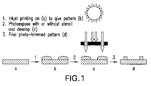
resolution lithographic mask. Briefly, the photo-trimming process relies on
the need to (1)
improve pattern edge acuity for inkjet printed features and/or (2) the desire
to pattern,
selectively, high resolution features using already printed patterns. Fig. 1
shows a
schematic that demonstrates the process for negative (crosslinking) tone.
The composition and methods of the present invention are useful in a variety
of
manufacturing processes including:
Compound Semiconductor manufacture: Lift-off in Transistors manufacture; PMGI
can
be used as a di-electric layer for passivation.
Lift-Off: Lift-off can be used for Controlled Metal deposition in compound
semiconductor applications such as photovoltaics, VCELs, transistors.
Optical Electronics, such as manufacturing of LEDs: deposition of
encapsulation /
passivation layer; metal deposition in a lift-off process; creation of a
background grating
for light reflection.
Energy Devices: Enable manufacture processes in Battery & Fuel Cell
applications
CA 02699920 2010-03-17
WO 2009/038766 PCT/US2008/010899
Displays: DLP Displays - Deposition of epoxy as support structure
MEMS: Sensors, actuators, resonators, microfluidic devices; PMGI can be used
as a
sacrificial layer support for use in 3D MEMS devices
Printed Wire Boards and Printed Circuit Boards: Etch resistance for processes
Passivation layer: Back-end Packaging of devices.
Photo-Trimming can be used to increase resolution for MEMS, Microfluidics,
Nano-
imprint and can be used to enhance any of the above applications.
I1
CA 02699920 2010-03-17
WO 2009/038766 PCT/US2008/010899
EXAMPLES
The following examples are intended to illustrate, but in no way limit the
scope of
the present invention. All parts and percentages are by weight and all
temperatures are in
degrees Celsius unless explicitly stated otherwise.
Example 1- Epoxy-based Composition 1
An epoxy (SU-8) composition was made by blending the following ingredients as
outlined above.
Component Amount (wt%)
Epoxy SU-8 Resin 27.8
PAG (Cyracure) 1.4
Flexiblizer (Polyol 3315) 3.25
Surfactant (FluoroN) 0.01
Solvent 1 (y-butyrolactone) 3.375
Solvent 2 (Methyl Isobutyl Ketone) 64.125
The above ingredients were combined as described above, printed onto a silicon
substrate, and cured as described above. Images from this composition were
examined by
electron microscopy and shown in Figs 1-4.
Example 2 - Epoxy-based Composition 2
A second epoxy (SU-8) composition was made by blending the following
ingredients as outlined above. When used with the Dimatix DMP-2800 Series 16
piezo-
print head printer, this composition produces thicker features for single pass
by changing
the solvent system
12
CA 02699920 2010-03-17
WO 2009/038766 PCT/US2008/010899
Component Amount (wt%)
Epoxy SU-8 Resin 29.5
PAG (Cyracure) 1.48
Surfactant (PF-151N) 0.1
Solvent 1 (y-butyrolactone) 6.9
Solvent 2 (Cyclopentanone) 62.1
The above ingredients were combined as described above, printed onto a silicon
substrate, and cured as described above. Images from this composition were
examined by
electron microscopy and shown in Figs 5-6.
Example 3 - Novolac Resin
A Novolac composition was made by blending the following ingredients as
outlined above.
Component Amount (wt%)
Novolac Resin 24.6
Crosslinker (Powderlink 1174) 4.67
TAG (CXC 1612) 0.31
Flexibilizer (Polyol 3315) 2.87
Surfactant (FluoroN) 0.025
Solvent I (y-butyrolactone) 4.725
Solvent 2 (Methyl Isobutyl Ketone) 62.775
The above ingredients were combined as described above, printed onto a silicon
substrate, and cured as described above. Images from this composition were
examined by
electron microscopy and shown in Figs 7-8.
Example 4 - PMGI Composition
A PMGI composition was made by blending the following ingredients as outlined
above.
13
CA 02699920 2010-03-17
WO 2009/038766 PCT/US2008/010899
Component Amount (wt%)
PMGI Resin 10.99
Surfactant (FluoroN) 0.01
Solvent 1 (y-butyrolactone) 50.7
Solvent 2 (Cyclopentanone) 32.1
Solvent 3 (1,3 Dioxolane) 6.2
The above ingredients were combined as described above, printed onto a silicon
substrate, and cured as described above.
Example 5 - Conducting Nanocomposite of Photopatterning Epoxy for Active
Matrix
Liquid Crystal Displays (AMLCD) and Active Matrix Organic Light Emitting Diode
Displays (AMOLED).
This ink jet epoxy composition incorporates nanosized conducting Indium Tin
Oxide (ITO) conducting nanocomposite (5-100nm diameter or monodisperse
nanospheres)
to ink jet pattern both rigid and flexible conducting transistors in pixels
for AMLCD and
AMOLED applications. Photo-Trimming is then employed to achieve resolution
required
for patterning the ITO transistor.
Component Amount (wt%)
Epoxy SU-8 Resin + 0.1-10 wt% ITO 29.5
nanopheres dispersed
PAG (Cyracure) 1.48
Surfactant (PF-151N) 0.1
Solvent 1 (y-butyrolactone) 6.9
Solvent 2 (Cyclopentanone) 62.1
The ITO nanospheres (0.1-10 wt%) are dispersed in a solution of 29.5 wt% Epoxy
SU-8 resin + 62.1 wt% Cyclopentanone. The remainder of the components are
serially
added and stirred at room temperature 12-24 hours. Thereafter, the whole is
filtered to 1
micron or better.
Example 6 -- Conductiniz Nanocomposite of Photopatterning Epoxy
14
CA 02699920 2010-03-17
WO 2009/038766 PCT/US2008/010899
Nanocomposite light blocking dielectric film consisting of Titanium Oxide
(TiO2)
nanospheres, (5-100nm) dispersed in photo and thermal hardening epoxy for
permanent
applications, using the general formulation recipe described in Example 5 and
substituting
TiO2 nanospheres for ITO nanospheres specifies this example.
Example 7 -- Conducting Nanocomposite of Photopatterning Epoxy
A nanocomposite barrier layer consisting of nanosized silica and/or zeolite
compositions (5-100nm sphere diameter), with photo or thermally hardened
epoxy, for use
as moisture resistant barrier layer. Using Example 5 as the basic recipe, and
substituting
nanosized silica and/or zeolite nanocomposite compositions for ITO specifies
this
example.
Example 8 -- Conducting Nanocomposite of Photopatterning Epoxy
A nanocomposite antimicrobial, antibacterial film layer consisting of a
nanosized
silver or silver nanocomposite compound, in 5-100mm nanospheres or equivalent,
with
photo or thermally hardened epoxy polymer.
Example 9 -- Photo-Trimming
The ink jet printed epoxy composition of Example 1 or 2 may be subsequently
patterned with UV light through a high resolution lithographic mask. To
implement this
process, a photo-mask is aligned to the printed area to product these images
as outlined
above. Two major features of photo-trimming are increased resolution and
reduction of
scum during processing. Photo-trimming can also be used in a Lift-off process
where a
printable PMGI compositions are layered with a printed epoxy or novolac
formulary to
image it and further increase resolution. Results of the photo-trimming
process are shown
in Figs. 9-14.
Example 10 - Lift Off Processes for Metal Deposition
As indicated above, Lift-Off processes can be used for controlled metal
deposition
in compound semiconductor applications such as photovoltaics, VCELs,
transistors. An
example of this technique using the compositions and processes of the present
invention is
shown in Figure 15.
CA 02699920 2010-03-17
WO 2009/038766 PCT/US2008/010899
A micrograph of a Lift-Off profile (Figure 15, Option 2) was created. The
underlayer was made from PMGI Ink printed and cured (Example 4), and cured at
110 C
for 1 min. This product was coated with a top layer comprising an epoxy ink
printed and
cured (Example 2), and then cured at 110 C for 1 min. Development time
(immersion)
was -1 min in 2.38% TMAH Developer.
16