Note: Descriptions are shown in the official language in which they were submitted.
CA 02700052 2010-03-18
PCT/EP2008/061977 - 1 -
2007P20374WOUS
Description
Power control device of a power supply system of an
electrochemical coating facility
The invention relates to a device for the power control of a
power supply system of an electrochemical coating facility.
In an electrochemical coating facility, workpieces are coated
locally or globally in respect of their area with material
layers by means of a potential difference being produced
between the workpiece to be coated and a medium in which the
coating material is dissolved, and/or between the medium and
external electrical conductors, which potential difference
leads indirectly to condensation of the coating material on the
workpiece. In addition to the change in the state of matter of
the coating material, the latter can also change chemically in
the course of the condensation process on the workpiece. The
medium can be in a liquid, gaseous or plasmatic state of matter
and can be the coating material itself, or can be a solvent or
transport medium which contains the coating material.
Known electrochemical coating methods comprise plasma coating
methods, for example, in which, in general, highly dilute gases
are ionized by high-field excitations and thereby put into a
plasmatic state of matter. As a result of chemical reactions in
the plasma, the reaction products can then deposit (sputtering)
on a substrate - in particular on a workpiece to be coated. A
further important subgroup of the electrochemical coating
methods is the electrolytic coating methods, in which ion
diffusions are induced in an electrically dissociable medium by
means of an externally applied electrical
CA 02700052 2010-03-18
PCT/EP2008/061977 - la -
2007P20374WOUS
potential, which can lead indirectly to material deposition on
a workpiece
CA 02700052 2010-03-18
PCT/EP2008/061977 - 2 -
2007P20374WOUS
introduced into the medium. In this way, in electroplating
technology, for example, workpieces are coated with metals by
means of melts or solutions of metal salts being
electrolytically separated. In this case, a - generally
metallic - workpiece is conductively connected to an electrode,
in particular a cathode, and an external electrical potential
is applied between the electrode and the corresponding other
electrode, in particular the anode. The positively charged
metal ions (cations) in the metal salt melt or solution migrate
to the cathode, are electrically neutralized upon contact with
the workpiece and deposit as metal atoms on the workpiece.
Coating methods in which workpieces are introduced into a
usually liquid medium for the purpose of coating are also known
as dipping bath coating methods.
In the case of an electrolytic dipping bath coating, the layer
application per unit time onto the workpiece to be coated is a
function of a number of parameters, which include, in
particular, the applied electrical potential, the time and the
thickness of the material layer already applied to the
workpiece. Firstly, there is a decrease in the ion
concentration in the medium given a constant potential in the
course of coating with time, and therefore, given chemical
properties that are otherwise kept constant, in particular the
ion concentration of the bath, there is also a decrease in the
current intensity of the ion current migrating to the cathode
and, consequently, the layer application per unit time. This
effect can be intensified if the material layer already applied
has an insulating effect, which is in turn dependent on the
conductivity of the cathode material, the time-dependent
conductivity of the medium with the ions and on the
conductivity of the layer material and also on the ratios of
these conductivities. When all of the influencing parameters
are taken into account, the layer
CA 02700052 2010-03-18
PCT/EP2008/061977 - 2a -
2007P20374WOUS
application per unit time generally decreases overall given a
constant electric potential, with the result that, in order to
form a temporally linear layer thickness increase onto the
workpiece, the electric potential has to be increased
continuously with the residence time.
CA 02700052 2010-03-18
PCT/EP2008/061977 - 3 -
2007P20374WOUS
In the case of commercial dipping bath coating facilities
designed for the coating of large workpieces, for example for
the coating of vehicle bodies, power units are generally
available for the DC voltage feeding the dipping bath, with
which power units, for technical reasons, only a few,
substantially constant potential values can be set. These
potential values are also referred to as voltage levels.
Furthermore, a change between the voltage levels in the dipping
bath in the course of a coating process unfavorably causes
discontinuities in the layer application; in particular, in the
event of a changeover from one voltage level to the next higher
voltage level, current spikes momentarily arise, which
adversely influences the coating quality. The or each voltage
level is generated from an externally supplied AC voltage by
means of the AC voltage being rectified and smoothed by means
of the supply system and circuit components. In this case, low-
pulse circuits are used, inter alia, for cost reasons, which
circuits, in comparison with higher-pulse circuits, are
significantly more cost-effective and require a comparably low
control outlay, but produce a higher proportion of reactive
power in the external supply system, whereby the supply system
is burdened and the operating costs of the coating facility are
increased. Moreover, in order to be able to prevent a
production outage caused by a failure of a power unit,
generally at least one reserve unit is installed, which is
linked to the external supply system via further supply system
and circuit components. However, by virtue of such redundant
components, which as a rule are not utilized, the costs for the
coating facility are furthermore increased.
Consequently, it is an object of the invention to specify a
power control device for an electrochemical coating facility
which is as cost-effective as possible and which ensures that
the coating facility is operated as
CA 02700052 2010-03-18
PCT/EP2008/061977 - 3a -
2007P20374WOUS
efficiently and reliably as possible, while at the same time
ensuring a high coating quality.
CA 02700052 2010-03-18
PCT/EP2008/061977 - 4 -
2007P20374W0US
The object of the invention is achieved by means of the
features of claim 1. Accordingly, a power control device of a
power supply system - which comprises a number of anodes and a
number of cathodes - of an electrochemical coating facility is
specified, having a plurality of control modules, wherein each
control module is designed to form and control a local current
flow having a predetermined magnitude as a function of the
location and as a function of the time between an anode and a
cathode of the power supply system.
A conventional dipping bath coating facility for vehicle bodies
usually comprises two to four power units. The first unit feeds
the dipping bath with a predetermined DC voltage. The current
intensity in the dipping bath and thus the layer application
per unit time decrease in the course of the coating process.
Starting from a specific point in time, the second power unit
is connected in, which feeds the bath with an increased
voltage, with the result that the layer application per unit
time increases again and thereby corresponds, on average over
time, to a predetermined (constant) value. The currents and
voltages present in the bath are subject to global boundary
conditions which limit a continuous controllability of the
electric potential present at the dipping bath and thus define
the (abovementioned) voltage levels. Consequently, threshold
values exist, for example, which are to be achieved in order to
ensure an effective layer application; on the other hand, limit
values also exist which must not be exceeded in order that no
partial discharges arise at the object to be coated. What is
relevant for ensuring a high coating quality, however, is a
layer application per unit time which is as constant as
possible for all points in time. However, the spatial
distribution of the layer thickness over the surface of
CA 02700052 2010-03-18
PCT/EP2008/061977 - 4a -
2007P20374W0US
the coated object is controllable only to a limited extent,
which is disadvantageous particularly when a spatially variable
layer application is intended to be effected in a targeted
manner.
CA 02700052 2010-03-18
PCT/EP2008/061977 - 5 -
2007P20374WOUS
Since both power units are fed by an AC voltage from an
external supply system, a power converter circuit with
rectifiers is set up, which converts the AC voltage/AC current
into a pulsed DC voltage/pulsed DC current. Buffer capacitances
and inductances are used to smooth the voltage and the current
by reduction and compensation of the fluctuation amplitudes.
On the supply system side, boundary conditions imposed on the
AC voltages and currents with regard to the amplitudes thereof
and the relative phase shifts thereof correspond to the
boundary conditions for the currents and voltages in the
dipping bath. In particular, specific minima for the phase
shift between AC voltage and AC current in the power converter
circuit are predetermined by the voltage levels in the dipping
bath. As a result, however, a so-called displacement reactive
power is produced in the supply system, which, in
correspondence to the minima of the phase shift, is reducible
in each case only to a specific value.
Furthermore, for cost reasons, low-pulse power converter
circuits are usually used, which, under load in the high-
frequency harmonic wave components of the AC voltages and
currents, the so-called harmonics, overall produce larger
amplitude contributions in the supply system than higher-pulse
power converter circuits. These harmonic contributions produce
an additional reactive power within the supply system.
The invention is based on the consideration, therefore, of
modularizing the power control for the bath-feeding power
supply system. A significant proportion of the inadequacies
with regard to the realizability of a uniform layer application
onto an object to be coated and also the irreducibility of the
reactive power which arises in the
CA 02700052 2010-03-18
PCT/EP2008/061977 - 5a -
2007P20374W0US
course of the bath power supply in the external supply system
can be attributed to the fact that a high global bath current
is produced with the aid of a small number of power units. The
number of variable
CA 02700052 2010-03-18
PCT/EP2008/061977 - 6 -
2007P20374WOUS
parameters is correspondingly small given defined boundary
conditions. In contrast thereto, with the aid of a higher
number of decoupled and separately drivable power and control
modules, in each case local currents can be formed between a
respective cathode and a respective anode in the bath and be
controlled. It is thereby possible, in particular, to realize
layer applications of different heights per unit time by means
of targeted driving in defined spatial zones of the bath; by
way of example, it is thereby possible, in the case of a
vehicle body, for the B-pillar to be coated to a greater extent
than the vehicle roof in the course of a coating process.
Equalization effects in the bath which endeavor to homogenize a
spatially and temporally defined distribution of the flow field
in the bath can be avoided or reduced by means of circuitry
measures and by means of a suitable circuit network topology.
The currents controlled by the individual control modules are
not subject to the same boundary conditions as a global bath
current, with the result that, in particular, the amplitudes
and the relative phase shifts of and respectively between the
AC voltages and currents present at the control modules on the
supply system side can be smaller. As a result, the
displacement reactive power in the supply system is reduced
overall. Furthermore, the harmonic components of the AC
voltages and currents which are caused by the individual
control modules which are decoupled from one another are
statistically independent of one another, such that, as a
result of a statistical interference of the waves, the
amplitude of the total reactive power in the supply system
which can be attributed to harmonic effects is significantly
reduced.
Furthermore, by virtue of a relatively large number of control
modules, there is no need for any additional
CA 02700052 2010-03-18
PCT/EP2008/061977 - 6a -
2007P20374WOUS
number of modules as reserve units. The system is already
highly redundant, and the failure of a control module during a
coating process therefore does not lead to significant
impairment of the process. Furthermore, it is possible for
individual control
CA 02700052 2010-03-18
PCT/EP2008/061977 - 7 -
2007P20374WOUS
modules or module groups to be selectively switched on or off
in the course of a coating formulation.
The consideration discussed above, on which the invention is
based, can be applied to the generalized case in which the
dipping bath is substituted by a medium of an electrochemical
coating facility of general type.
In one advantageous embodiment of the power control device, a
or each control module comprises a circuit arrangement having a
number of power converters, in particular having a number of
rectifiers. By means of a rectifier, an AC current from the
external supply system is converted to a DC current with which
the dipping bath is fed. By means of a united and iteratively
extendable circuit arrangement comprising a plurality of
rectifiers, in particular in a parallel circuit, a high pulse
number can be achieved, whereby the proportion of harmonics of
such a circuit is iteratively reduced in a corresponding
manner. The pulse number describes the number of coperiodic
voltage or current waves which are triggered within a wave
period, and the relative phase shift between two successive
partial waves is given here by the period duration divided by
the pulse number.
Preferably, a or each power converter, in particular a or each
rectifier, is connected to a number of anodes or cathodes of
the power supply system. In the case of an electrolytic coating
facility for coating with metals, the object that is
respectively to be coated is conductively connected to a
cathode and the coupling of the or each power converter is
preferably effected anodally.
In an advantageous manner, a or each circuit arrangement of
power converters is realized as a series circuit formed by a
controlled rectifier and an uncontrolled rectifier.
CA 02700052 2010-03-18
PCT/EP2008/061977 - 7a -
2007P20374WOUS
This local circuit topology is based on the principle of a so-
called boost and buck connection, by means of which
CA 02700052 2010-03-18
PCT/EP2008/061977 - 8 -
2007P20374WOUS
the phase shift between AC voltage and current is optimized on
the supply system side during load operation, and a
correspondingly low displacement reactive power is thus
realized.
In one expedient development of the circuit arrangement of
power converters, a or each controlled rectifier is realized as
a thyristor bridge and/or a or each uncontrolled rectifier is
realized as a diode bridge. Such a combination has the
advantage that an uncontrolled diode bridge is significantly
more cost-effective than a controlled power converter.
Preferably, the power control device is designed to the effect
that a or each control module is connected to a number of
isolation transformers.
In a particularly advantageous embodiment of the power control
device, a or each controlled rectifier is connected to a
respective isolation transformer and a or each diode bridge is
connected to a respective further isolation transformer.
Such an embodiment is realized for example in the case of a
circuit arrangement in which a diode bridge and a controlled
rectifier which are connected in series with one another are
connected to a first and second isolation transformer,
respectively. The first isolation transformer feeds the diode
bridge with a first current, which is in phase with the
external AC voltage, and the second isolation transformer feeds
the controlled rectifier with a second current, which is phase-
shifted by 30 degrees with respect to the first current on the
supply system side. Such a 12-pulse feeding, that is to say a
feeding that is phase-offset by 30 degrees in each case, of
this rectifier circuit can be realized for example with a first
CA 02700052 2010-03-18
PCT/EP2008/061977 - 8a -
2007P20374WOUS
isolation transformer of vector type DyO and with a second
isolation transformer of vector type Dy5 from a 6-pulse energy
feed in which the phase shifts are 60 degrees in each case. A
relatively cost-effective
CA 02700052 2010-03-18
PCT/EP2008/061977 - 9 -
2007P20374W0US
12-pulse rectifier circuit is thus presented, which is
advantageous with respect to a low-pulse rectifier circuit, in
particular with respect to a 6-pulse rectifier circuit, with
regard to the total harmonic generation.
If, by contrast, a 12-pulse feeding is already available on the
supply system side, then the isolation transformers can be
embodied identically in respect of their type, for example as
isolation transformers of vector type DyO.
In addition to the total reduction of the harmonic components
which result from the statistical independence and thus from
the statistically uniformly distributed interference of the
harmonic fluctuations which are triggered by the individual
control modules, an additional reduction of the harmonics that
have a perturbing effect on the external supply system is
achieved by virtue of the fact that their amplitudes scale
inversely proportionally to the number of control modules.
Consequently, a particularly effective reactive power reduction
is achieved overall with the displacement reactive power
reduction. Consequently, the power factor of the power control
device, which describes the ratio of the effectively utilized
active power to the total power in the supply system including
the reactive power, can attain for example a value of more than
0.94, and, in the case of a rated load of 12.5%, even more than
0.8. The reactive power reduction leads, in particular, to
relief of the loading of the feeding supply system
transformers.
By virtue of a 12-pulse rectifier circuit, on the DC side twice
as many current and voltage maxima as in the case of 6-pulse
driving arise. The amplitudes of the maxima are likewise
smaller. Consequently, the DC current produced by the 12-pulse
rectifier circuit and the DC voltage have
CA 02700052 2010-03-18
PCT/EP2008/061977 - 9a -
2007P20374WOUS
comparatively small fluctuations. In the case of a suitable 12-
pulse rectifier circuit, the fluctuation amplitude can be less
than 1% of the DC current intensity or DC voltage produced. The
required
CA 02700052 2010-03-18
PCT/EP2008/061977 - 10 -
2007P20374WOUS
buffer capacitances and inductances for DC voltage smoothing
and for DC current smoothing, respectively, which are realized
for example by a smoothing capacitor and a DC inductor,
respectively, can therefore advantageously be made smaller than
in the case of a low-pulse rectifier circuit, with the result
that overall the efficiency and the economic viability of the
power control device are increased.
In a further advantageous embodiment variant of the power
control device, a decoupling circuit is formed between a or
each control module and in each case a number of anodes, which
decoupling circuit decouples the respective control module from
the dipping bath. The decoupling circuit comprises a plurality
of diodes connected in series, which diodes are in each case
connected in the forward direction to a respective anode.
A return-flow compensation is realized with the aid of such a
decoupling circuit with the result that a flow field set in a
defined manner in the bath between the anodes and cathodes does
not collapse and/or is homogenized. Equalizing currents between
locally adjacent feed locations are prevented.
Preferably, the decoupling circuit comprises a series circuit
formed by a first diode and a second diode, which is in each
case connected in the forward direction to a first anode and/or
to a second anode, wherein the first diode is connected in the
reverse direction to the control module via a switching element
and an inductance, and wherein the second diode is connected in
the reverse direction to the first diode, to the first anode
and to a smoothing capacitor.
CA 02700052 2010-03-18
PCT/EP2008/061977 - l0a -
2007P20374WOUS
The current for both anodes flows via the first diode, and only
the current for the second anode flows via the second diode.
The voltage drop respectively at the first and at the second
diode can lead to different voltages at the first and at the
second anode. This voltage difference
CA 02700052 2010-03-18
PCT/EP2008/061977 - 11 -
2007P20374WOUS
is compensated for by the fact that the cable path for an anode
via the bath is inevitably longer, however.
The provision of a smoothing capacitor between the two series-
connected diodes of the decoupling circuit has the advantage
that no resonant circuit can arise between the smoothing
capacitor and the inductance required for smoothing the total
current flow, said inductance being provided as a DC inductor
coil, in particular. The smoothing capacitor is charged by the
power converter circuit via the inductance and also via the
first diode in the forward direction. Return oscillation of the
energy from the smoothing capacitor to the diode is not
possible, however, as a result of the blocking effect of the
diode. Therefore, the energy can only discharge via the
resistance of the bath. In particular, undesirable equalizing
discharge and compensation processes within the bath are thus
prevented. Furthermore, damping that would be required for a
resonant circuit, and exhibits loss of energy, is not required.
A computing unit with a simulation model for simulating voltage
and/or current predeterminations is expediently set up for the
power control device. Such a simulation calculates, in
particular, voltage and current predeterminations in the bath
and the parameters dependent thereon for a coating process. The
definition of location-dependent desired coating thicknesses in
a CAD representation of the object to be coated is produced by
an operating program used for predetermining the voltage and/or
the current that is output to the bath via an or each anode, as
a function of the object position in the bath.
An exemplary embodiment of a power control device according to
the invention of a power supply system of an
CA 02700052 2010-03-18
PCT/EP2008/061977 - 11a -
2007P20374WOUS
electrochemical coating facility is explained below with
reference to a drawing, in which:
CA 02700052 2010-03-18
PCT/EP2008/061977 - 12 -
2007P20374WOUS
Fig. 1 shows a circuit diagram of the power control device in
schematic illustration, and
Fig. 2 shows a further circuit diagram of the power control
device in schematic illustration.
Mutually corresponding parts in different figures are provided
with the same reference symbols.
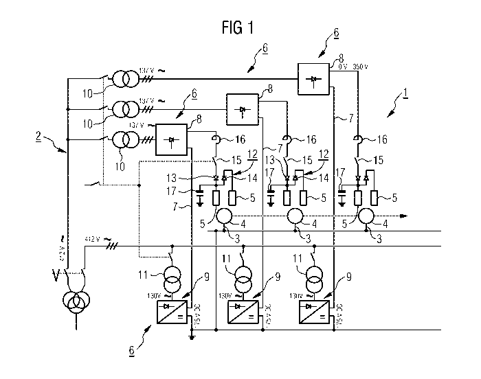
Fig. 1 schematically illustrates a circuit diagram of a power
control device 1 of a power supply system 2 of an
electrochemical coating facility.
The potential matching indicated by the coating process takes
account of the matching of the secondary voltage of the
isolation transformers. It brings about an additional
optimization of the reactive power component in the driving
supply system.
The power supply system 2 comprises a plurality of cathodes 3,
which are conductively connected to a number of objects 4 to be
coated, and also a plurality of anodes 5 respectively grouped
in pairs. The cathodes 3 with the objects 4 to be coated and
the anodes 5 are introduced into a dipping bath containing a
metal salt solution.
The power control device 1 comprises a number of control
modules 6 each having a series circuit 7 formed by a controlled
thyristor bridge 8 and an uncontrolled diode bridge 9. Both the
thyristor bridge 8 and the diode bridge 9 are connected to a
respective three-phase isolation transformer 10 and 11 on the
supply system side. The thyristor bridge 8 is connected in the
forward direction to a pair of anodes 5 via a decoupling
circuit 12. The decoupling circuit 12 comprises a first and a
second diode 13 and 14, respectively, which are in each case
connected
CA 02700052 2010-03-18
PCT/EP2008/061977 - 12a -
2007P20374WOUS
in the forward direction to an anode 5 of the pair of anodes 5.
The first diode 13 is connected in the reverse direction to the
thyristor bridge 8 via a switching element 15 and a DC inductor
16, and the second
CA 02700052 2010-03-18
PCT/EP2008/061977 - 13 -
2007P20374WOUS
diode 14 is connected in the reverse direction to the first
diode 13 and to the anode 5 connected thereto in the forward
direction, and also to a smoothing capacitor 17.
The isolation transformers 10 and 11 feed the thyristor bridge
8 and the diode bridge 9, respectively, with an AC voltage in
each case, wherein the AC voltages are in phase, or have a
phase angle of 30 degrees with respect to one another. The
series circuit 7 formed by thyristor bridge 8 and diode bridge
9 produces therefrom and from the AC current of identical
frequency that arrives via the isolation transformers 10 and 11
a pulsed DC voltage and a pulsed DC current, respectively, the
fluctuation amplitudes of which are smoothed with the aid of
the smoothing capacitor 17 and by means of the DC inductor 16,
respectively. In this case, the formation of an LC resonant
circuit from the DC inductor 16 and the smoothing capacitor 17
is prevented by the first diode 14 of the decoupling circuit
12, said first diode being arranged in intervening fashion in
terms of circuit technology, since the energy stored in the
electric field of the smoothing capacitor 17 cannot flow back
as a current in the reverse direction of the first diode 14 to
the DC inductor 16. Equalizing effects of the fields between
the cathodes 3 and the anodes 5 are avoided by means of the
decoupling circuit 12.
Fig. 2 shows a further circuit diagram of the power control
device shown in Fig. 1 according to Fig. 1 in schematic
illustration.
What can be seen are the control modules 6 having the thyristor
bridges 8 and the diode bridges 9, which are connected to the
power supply system 2 by means of the isolation transformers 10
and 11, respectively, and which are connected to the anodes 5
on the bath side. In contrast to
CA 02700052 2010-03-18
PCT/EP2008/061977 - 13a -
2007P20374WOUS
Fig. 1, the pairs of anodes 5 illustrated therein, which are
connected to a respective control module 6, are depicted
schematically as a unit in this illustration. The decoupling
circuits 12 illustrated in Fig. 1 are not illustrated here. The
region of the dipping bath 18 is identified by a separating
line 19.
CA 02700052 2010-03-18
PCT/EP2008/061977 - 14 -
2007P20374WOUS
DC voltages and DC current flows of different magnitudes are
respectively present at the anodes 5 depending on their linear
position with respect to the dipping bath 18, in order to
obtain a uniform layer application on a vehicle body that is
guided past the anodes 5 in the dipping bath 18. The thyristor
bridges 8 and the diode bridges 9 of the control modules 6
which are connected to the respective anodes 5 produce these
respective DC voltages and DC currents from AC voltages and AC
currents, respectively, which are provided by the isolation
transformers 10 and 11, respectively, with the amplitude
respectively required. Depending on the position with regard to
the dipping bath 18, therefore, the isolation transformers 10
and 11 are respectively designed for transforming voltage
differences of different magnitudes.
The further details of the illustration correspond to the
details of the illustration in Fig. 1 and can be gathered from
Fig. 1.
The control modules can be connected in parallel in any desired
number for the purpose of increasing current, wherein the
interconnection can be embodied according to the master-slave
principle, in particular. Conventional systems of ADC (anodic
dip coating) and CDC (cathodic dip coating) embodiment can thus
be simulated identically. Mixed operation of ADC and CDC is not
ruled out.
The DC circuit is composed, in particular, of the series
circuit formed by unregulated and regulated power converters,
and also of storage elements (L and C) . The application also
covers any desired order of these elements in the series
circuit. By way of example, the order of controlled bridge,
inductance, uncontrolled bridge, capacitive smoothing, diode is
conceivable.
CA 02700052 2010-03-18
PCT/EP2008/061977 - 14a -
2007P20374WOUS
In order to further reduce the 12-pulse supply system
perturbations, in particular two systems can be connected in
series, the isolation transformers of which are offset by an
angle of 15 degrees with respect to the first system.