Note: Descriptions are shown in the official language in which they were submitted.
CA 02700108 2014-06-19
=
OPTICAL FIBER STRUCTURE, SYSTEM FOR FABRICATING THE SAME, AND
BLOCK-LIKE CHIP FOR USE THEREIN
TECHNICAL FIELD
The present invention relates to optical fiber structures, systems for
fabricating the
same, and block-like chips for use therein.
BACKGROUND ART
Laser guides have been widely used, as optical fiber components for
transmitting
laser beams with high energy density, for machining equipment, etc.
PATENT DOCUMENT 1 describes such a laser guide configured so that an
optical fiber for a laser guide is coaxially joined at at least one end with a
cylindrical block-
like chip (rod) having a greater diameter than the optical fiber.
However, for the laser guide described in PATENT DOCUMENT 1, the area of an
end face of the optical fiber is significantly different from that of an end
face of the block-
like chip, and thus the optical fiber and the block-like chip have drastically
different heat
capacities. This makes it difficult to fuse the optical fiber and the block-
like chip together
using electric discharge, a burner, etc. Therefore, the laser guide has poor
workability,
resulting in low productivity.
PATENT DOCUMENT 1: United States Patent No. 5,619,602
1
CA 02700108 2014-12-12
=
SUMMARY OF THE INVENTION
Certain exemplary embodiments can provide an optical fiber structure
comprising:
an optical fiber; and a block-like chip joined to the optical fiber, wherein
the block-like chip
is tapered toward a fiber-joined end of the block-like chip, and at least an
outer
circumferential surface of a distal portion of the block-like chip is
roughened.
Certain exemplary embodiments can provide a system for fabricating an optical
fiber
structure configured so that a block-like chip that is tapered toward a fiber-
joined end of the
block-like chip, and which block-like chip has a length of 5mm to 30 mm is
joined to an
optical fiber, the system comprising: a chip retainer for retaining the block-
like chip; a fiber
retainer for retaining the optical fiber; a moving member for relatively
moving the chip
retainer and the fiber retainer so that the block-like chip retained by the
chip retainer and the
optical fiber retained by the fiber retainer are in coaxial contact with each
other; a heater for
heating the block-like chip retained by the chip retainer and the optical
fiber retained by the
fiber retainer; and an axial relationship observer for observing, from an end
of the block-like
chip opposite to a fiber-joined end of the block-like chip retained by the
chip retainer, an
axial relationship between the fiber-joined end of the block-like chip and an
end of the
optical fiber.
Certain exemplary embodiments can provide a block-like chip used while being
joined to an optical fiber, and tapered toward a fiber-joined end of the block-
like chip,
wherein at least an outer circumferential surface of a distal portion of the
block-like chip is
roughened.
2
CA 02700108 2014-06-19
An optical fiber structure of another embodiment includes: an optical fiber;
and
a block-like chip joined to the optical fiber. The block-like chip is tapered
toward a fiber-
joined end of the block-like chip.
A system for fabricating an optical fiber structure of the present invention
is
directed to a system for fabricating an optical fiber structure configured so
that a block-like
chip is joined to an optical fiber. The system includes: a chip retainer for
retaining the
block-like chip; a fiber retainer for retaining the optical fiber; a moving
member for
relatively moving the chip retainer and the fiber retainer so that the block-
like chip retained
by the chip retainer and the optical fiber retained by the fiber retainer are
in coaxial contact
with each other; a heater for heating the block-like chip retained by the chip
retainer and the
optical fiber retained by the fiber retainer; and an axial relationship
observer for observing,
from an end of the block-like chip opposite to a fiber-joined end of the block-
like chip
retained by the chip retainer, an axial relationship between the fiber-joined
end of the block-
like chip and an end of the optical fiber.
A block-like chip of the present invention is used while being joined to an
optical
fiber, and is tapered toward a fiber-joined end of the block-like chip.
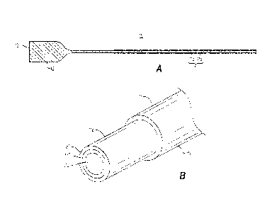
BRIEF DESCRIPTION OF THE DRAWINGS
[FIGS. 1A and 1B] FIG. 1A is a side view illustrating an optical fiber
structure;
FIG. 1B is a perspective cross-sectional view illustration the layers of an
optical fiber
structure.
[FIG. 2] FIG. 2 is a side view illustrating a block-like chip.
3
CA 02700108 2014-06-19
[FIG. 3] FIG. 3 is a diagram illustrating the configuration of a system for
fabricating an optical fiber structure.
DESCRIPTION OF EMBODIMENTS
An embodiment will be described hereinafter in detail with reference to the
drawings.
FIGs. 1A and 1B illustrate an optical fiber structure 10 according to this
embodiment. This optical fiber structure 10 is used while being incorporated
into a laser
guide for machining equipment, etc.
This optical fiber structure 10 includes an optical fiber 11 a, and a block-
like chip
12 joined to at least one end of the optical fiber 11 a.
The optical fiber lla includes a high refractive index core 11 a' forming the
core of
the optical fiber 11 a and made of pure quartz, and a low refractive index
clad 1 la" formed
integrally with the core to cover the core and made of quartz doped with
fluorine, etc. The
optical fiber 11 a may include a support layer 111a" formed integrally with
the clad 11 a" to
cover the clad and made of pure quartz. The optical fiber lla has, for
example, a length of
5 mm-300 m, an outer diameter of 125-1500 pm, and a core diameter of 50-1200
1.,tm. When
the optical fiber 1 la includes a support layer lla", the clad 11a" has, for
example, a
thickness of 3-90 i.tm, and the support layer 1 la" has, for example, a
thickness of 5-60 m.
For example, the refractive index of the core 11 a' of the optical fiber 11 a
is 1.458, and the
refractive index of the clad lla" thereof is 1.440-1.454. When the optical
fiber lla includes
a support layer 11 a", the refractive index of the support layer 11 a" is
1.458. The optical
4
CA 02700108 2014-06-19
fiber Ila and a coating layer I 1 b coating the optical fiber 1 la and made of
a UV curable
resin, etc., may form a coated optical fiber 11.
FIG. 2 illustrates a block-like chip 12.
A distal portion 12a of the block-like chip 12 is formed in a cylindrical
shape or
any other shape. A proximal portion 12b of the block-like chip 12 is formed in
a
bottleneck shape so as to be tapered toward the corresponding chip end. The
end face of
the chip 12 corresponding to the proximal portion 12b is formed parallel to
the end face of
the chip 12 corresponding to the distal portion 12a. The end face of the chip
12
corresponding to the proximal portion 12b is joined to an end face of the
optical fiber lla by
fusing them together. In other words, the end face of the block-like chip 12
corresponding
to the distal portion 12a forms a light entrance or a light exit, and the end
of the chip 12
corresponding to the proximal portion 12b forms the fiber-joined chip end to
be joined to the
optical fiber lla. This configuration allows light beams to enter and exit
from the end face
of the block-like chip 12 corresponding to the distal portion 12a. The chip
end face
corresponding to the distal portion 12a is wider than the end face of the
optical fiber 11 a.
As such, even when the intensity and density of incoming and outgoing light
are reduced,
the light beams are collected into the optical fiber 11 a, and thus the
optical fiber 11 a can
transmit high-intensity and high-density light beams. In view of the above,
the optical
fiber 11 a can be prevented from being damaged due to direct entrance and exit
of high-
intensity and high-density light beams into and from the end face of the
optical fiber 11 a.
The tapered shape of the proximal portion 12b of the block-like chip 12 is not
limited to a
bottleneck shape. The proximal portion 12b may be tapered to provide a cone or
any other
shape.
5
CA 02700108 2014-06-19
As illustrated in FIG. 2, the end face of the block-like chip 12 corresponding
to the
distal portion 12a, i.e., the light entrance end face or light exit end face
of the chip 12, may
be coated with an AR coating (anti-reflection coating) 13. When the end faces
of the
optical fiber 11 a are coated with AR coatings, the entire coated optical
fiber 11 needs to be
placed into an evaporator. Alternatively, a special evaporator needs to be
used. In the
former case, the process efficiency is low, resulting in poor productivity. In
the latter case,
an evaporator needs to be modified. However, with a configuration as described
above,
only many block-like chips 12 can be placed into a general-purpose evaporator
before fusing
with optical fibers 11 a, thereby depositing AR coatings 13 on the block-like
chips 12. The
AR coatings 13 include, for example, an Hf02-Si02 film, a Ta205-Si02 film, an
A1203-Si02
film, and an Nb205-Si02 film.
Furthermore, at least the outer circumferential surface of the distal portion
12a of
the block-like chip 12 may be roughened by sandblasting, etc. With such a
structure, when
stray light, etc., has entered the light entrance end face of the chip 12 from
outside, the stray
light, etc., can be allowed to escape to the outside without being reflected
off the light
entrance end face.
The block-like chip 12 has, for example, a length of 5-30 mm. The outer
diameter D of the end face of the block-like chip 12 corresponding to the
distal portion 12a
is, for example, 1-25 mm, and the outer diameter d of the end face of the
block-like chip 12
corresponding to the proximal portion 12b is, for example, 0.2-3 mm. When, as
illustrated
in FIG. 2, the length of the distal portion 12a of the block-like chip 12 is
denoted by the
character "A", the length of the tapered proximal portion 12b thereof is
denoted by the
character "B", and the spread angle of the proximal portion 12b is denoted by
the symbol
6
CA 02700108 2014-06-19
"0", they are preferably set to satisfy the following conditions: the
divergence angle 0. of
light from the optical fiber 11 a is equal to or less than the spread angle 0;
and the beam
diameter D' of the light at the end face of the block-like chip 12
corresponding to the distal
portion 12a is equal to or less than the outer diameter D. The divergence of a
laser beam
depends on the numerical aperture (NA) of the optical fiber 1 I a. In view of
the above, the
length A is, for example, 1-29 mm, the length B is, for example, 1-29 mm, and
the spread
angle 0 is, for example, 10-25 . In terms of the workability in retention of
the block-like
chip 12 to be fused with the optical fiber 11 a in a V-groove, etc., the
length A is preferably
equal to or greater than 1 mm.
Such an optical fiber structure 10 itself can be used as an optical element.
Furthermore, when an optical fiber structure is configured so that an optical
fiber lla has a
relatively short length of 5-100 mm and a block-like chip 12 is joined only to
one end of the
optical fiber 11 a, the optical fiber structure can be used as an optical
component. With use
of this optical component, the connection between the other end of the optical
fiber 11 a and
one end of another optical fiber 11 a can easily provide a new optical fiber
structure 10
configured so that the resultant optical fiber is provided at one end with the
block-like chip
12.
The optical fiber structure 10 configured as described above can be formed by
bringing the fiber-joined end of the block-like chip 12 and an end of the
optical fiber lla in
contact with each other while heating them.
For this optical fiber structure 10, the block-like chip 12 is formed so as to
be
tapered toward the fiber-joined end of the block-like chip 12 as described
above. This
reduces the difference between the area of an end face of the optical fiber 11
a and that of the
7
CA 02700108 2014-06-19
fiber-joined end face of the block-like chip 12. Therefore, the respective
heat capacities of
the optical fiber 11 a and the block-like chip 12 are close to each other.
This can facilitate
fusing the end faces together. As a result, high productivity can be achieved.
Here, since the heat capacity of the fiber-joined end of the block-like chip
12 is
preferably close to that of an end of the optical fiber 11a, the outer
diameter of the fiber-
j oined end face of the block-like chip 12 is preferably 1-5 times greater
than that of the end
face of the optical fiber 1 la.
Furtheimore, the optical fiber lla preferably has a three-layer structure of a
core, a
clad, and a support layer rather than a two-layer structure of a core and a
clad because, with
this three-layer structure, deformation of the optical fiber lla due to
heating for joining the
optical fiber 1 la to the block-like chip 12 has a negligible effect on the
core and the clad.
Next, an optical fiber structure fabrication system 20 will be described.
FIG. 3 illustrates the configuration of the optical fiber structure
fabrication
system 20.
The optical fiber structure fabrication system 20 includes a horizontal
rectangular
parallelepiped shaped stage body 21. The length directions of this stage body
21 are
denoted by X directions, the height directions thereof is denoted by Y
directions, and the
width directions thereof is denoted by Z directions.
The stage body 21 is provided at one end with a fiber retainer 22 for
retaining an
optical fiber 11a, and provided at the other end with a chip retainer 23 for
retaining a block-
like chip 12.
8
CA 02700108 2014-06-19
The fiber retainer 22 is provided on a structure obtained by stacking an X-
direction movable member 24 movable in the X directions, a Y-direction movable
member
25 movable in the Y directions, and a Z-direction movable member 26 movable in
the Z
directions in bottom-to-top order. The fiber retainer 22 includes a pair of
upper and lower
members. V-grooves are formed in the lower surface of the upper member and the
upper
surface of the lower member, respectively. A coated optical fiber 11 drawn
from a bobbin
is sandwiched between the upper and lower members so as to be retained in
these V-grooves.
The chip retainer 23 also includes a pair of upper and lower members. V-
grooves are formed in the lower surface of the upper member and the upper
surface of the
lower member, respectively. A distal portion 12a of the block-like chip 12 is
sandwiched
between the upper and lower members so as to be retained in these V-grooves.
A heater 27 is provided on a region of the stage body 21 between the fiber
retainer
22 and the chip retainer 23.
The heater 27 includes a movable member 28 movable in the X, Y, and Z
directions, and a heater body 29 provided on the movable member 28 to produce
a flame by
gas or arc discharge. The heater 27 is connected to a heating adjuster 30 for
adjusting the
intensity of the flame.
The optical fiber structure fabrication system 20 includes a Y-direction
observation camera 32 disposed above the location where the optical fiber 11 a
and the
block-like chip 12 are joined together, a Z-direction observation camera 33
and a Z-direction
magnification observation camera 34 both disposed lateral to the above-
described location,
and an X-direction observation camera (axial relationship observer) 31
disposed opposite to
the fiber-joined end of the block-like chip 12 retained by the chip retainer
23.
9
CA 02700108 2014-06-19
The Y-direction observation camera 32, the Z-direction observation camera 33,
the Z-direction magnification observation camera 34, and the X-direction
observation
camera 31 each include a CCD camera. The Y-direction observation camera 32,
the Z-
direction observation camera 33, and the Z-direction magnification observation
camera 34
each observe the axial relationship between the fiber-joined end of the block-
like chip 12
and an end of the optical fiber 11 a from a direction perpendicular to the
axis of the fiber.
The X-direction observation camera 31 observes the axial relationship between
the fiber-
joined end of the block-like chip 12 and the chip-joined end of the optical
fiber 1 la to be
joined to the block-like chip 12 from an axial direction of the fiber.
The Y-direction observation camera 32, the Z-direction observation camera 33,
the Z-direction magnification observation camera 34, and the X-direction
observation
camera 31 are each connected to a monitor 35. The monitor 35 has a screen
divided into
four sections. An image captured by each of these cameras is displayed on the
corresponding one of the four sections.
Next, a method for fabricating an optical fiber structure 10 using the optical
fiber
structure fabrication system 20 will be described.
First, a coated optical fiber 11 is retained by a fiber retainer 22 so that an
optical
fiber 11 a exposed by separating a coating layer 11 b from the optical fiber
11a protrudes
inwardly. A block-like chip 12 is retained by a chip retainer 23 so that a
tapered proximal
portion 12b of the block-like chip 12 protrudes inwardly.
Next, the optical fiber lla retained by the fiber retainer 22 is positioned
using an
X-direction movable member 24, a Y-direction movable member 25, and a Z-
direction
movable member 26 so that an end face of the optical fiber 1 1 a is opposed to
the fiber-
CA 02700108 2014-06-19
joined end face of the block-like chip 12 retained by the chip retainer 23. In
view of the
above, the X-direction movable member 24, the Y-direction movable member 25,
and the Z-
direction movable member 26 form moving members. In the above-mentioned
positioning,
images captured by a Y-direction observation camera 32, a Z-direction
observation camera
33, a Z-direction magnification observation camera 34, and a X-direction
observation
camera 31 are viewed on the screen of a monitor 35, thereby identifying the
axial
relationship between the fiber-joined end of the block-like chip 12 and the
end of the optical
fiber 1 I a.
Next, a heater 27 is positioned between the end of the optical fiber 1 la and
the
fiber-joined end of the block-like chip 12 by a movable member 28.
Next, the end of the optical fiber 11 a and the fiber-joined end of the block-
like
chip 12 are heated by the heater 27. The fiber retainer 22 is moved by the X-
direction
movable member 24, and the end of the optical fiber lla is thus brought
gradually closer to
the fiber-joined end of the block-like chip 12 retained by the chip retainer
23 to provide
contact therebetween, thereby fusing the optical fiber 1 1 a and the block-
like chip 12
together. In this case, images captured by the Y-direction observation camera
32, the Z-
direction observation camera 33, the Z-direction magnification observation
camera 34, and
the X-direction observation camera 31 are again viewed on the screen of the
monitor 35,
thereby identifying the axial relationship between the fiber-joined end of the
block-like chip
12 and the end of the optical fiber lla.
11
CA 02700108 2014-06-19
Subsequently, the heating of the heater 27 is stopped, and the fiber retainer
22 is
moved by the X-direction movable member 24, thereby applying a slight tension
to a fused
portion of a resultant optical fiber structure 10 where the optical fiber 11 a
and the block-like
chip 12 are fused together.
Thereafter, the fiber retainer 22 and the chip retainer 23 terminate the
retention of
the optical fiber 11 a and the block-like chip 12. Thus, the optical fiber
structure 10 is taken
out of the retainers 22 and 23.
A fiber splicer for joining optical fibers together can align the optical
fibers by
identifying the axial relationship between the respective ends of the optical
fibers from a
direction perpendicular to the axes of the optical fibers, but cannot align
the optical fibers by
identifying the above-described axial relationship from axial directions of
the optical fibers.
However, since the optical fiber structure fabrication system 20 is provided
with the X-
direction observation camera 31, it can align the optical fiber lla and the
block-like chip 12
by identifying the axial relationship between the fiber-joined end of the
block-like chip 12
and the end of the optical fiber 11 a from respective axial directions of the
optical fiber 1 1 a
and the block-like chip 12. This enables determination of the quality of the
fusion
deteriorated by air bubbles in the fused portion of the optical fiber
structure 10, and
deformation of the end face of the optical fiber lla. Furthermore, if
necessary, air bubbles
can be removed from the fused portion by further heating the fused portion.
Alternatively,
the fused portion can be shrunk.
12
CA 02700108 2014-06-19
_
INDUSTRIAL APPLICABILITY
The present invention is useful for optical fiber structures, systems for
fabricating
the same, and block-like chips for use therein.
13