Note: Descriptions are shown in the official language in which they were submitted.
CA 02701432 2010-04-27
CONNECTING ELEMENT FOR ELECTRIC CONDUCTORS WITH A
PRINTED CIRCUIT BOARD
BACKGROUND OF THE INVENTION
1. Field of the Invention
The invention pertains to an electric connecting element consisting of an
electric contact, a housing and a clamping pin for separably mounting an
electric conductor on an opening of a printed circuit board.
2. Description of the related art
Connecting elements of this type are required for contacting an electric con-
ductor at any location on a printed circuit board. In this case, optimal
electric
contacting between the printed circuit board and the connecting element
needs to be ensured by means of a flawless mechanical seat of the connect-
ing element on the printed circuit board.
US 7,290,344 B2 discloses a method for connecting an electric conductor to
a metal plate, wherein a cable lug radially expands a sleeve in a hole in the
metal due to a screwed connection and thusly produces an electric connec-
tion.
DE 197 49 890 C1 discloses an electronic contact element that is provided
with a central bore and axial slots on the mounting end, wherein elastic tabs
CA 02701432 2010-04-27
2
are formed and these tabs are pressed radially outward when pressing in a
pressure piece.
DE 10 2004 020 422 Al discloses a pin for producing a solderless electric
connection with a printed circuit board, with a press-fit region that can be
elastically and plastically deformed in a hole of the printed circuit board in
order to be adapted to the hole diameter. A press-fit tool that guides and re-
inforces the pin is provided for the insertion of the pin.
Permanent connections between a connecting element and a printed circuit
board such as, for example, riveted connections are frequently utilized. In
variations that utilize screwed or soldered connections for separably connect-
ing a connecting element to printed circuit boards, a special tool is required
for mounting and also for dismounting the element. The dismounted con-
is necting element frequently cannot be reused due to a destructive dismount-
ing.
SUMMARY OF THE INVENTION
The invention therefore is based on the objective of designing a connecting
element in such a way that reliable contacting of an electric conductor on a
printed circuit board is ensured without the aid of tools by means of an elec-
tric contact. It should furthermore be possible to dismount the connecting
element from the printed circuit board in a non-destructive fashion in order
to
exchange and to reuse the connecting element and the printed circuit board.
This objective is attained in that the electric contact features a sleeve-like
contact region that can be inserted into an opening in the printed circuit
board and radially clamped against the inner surface of the opening by in-
serting a clamping pin into the sleeve-like contact region, and in that the
electric contact features a terminal region with a termination for mounting
the
electric conductor.
CA 02701432 2010-04-27
3
The invention concerns an electric connecting element consisting of an elec-
tric contact, a housing and a clamping pin. The electric contact features a
contact region and a terminal region. Contacting on a printed circuit board is
realized by inserting the contact region into an opening in the printed
circuit
board, wherein at least the inner surface of the opening is provided with an
electric contact area. The electric contact area preferably is
circumferentially
arranged on the opening in an L-shaped fashion such that electric contacting
on the printed circuit board can also be realized around the opening.
In the contact region, the electric contact of the connecting element is real-
ized in the form of a sleeve-like part with a bulgy distention and features at
least one axial slot. The diameter of this sleeve-like contact region is
elasti-
cally reduced in the axial direction during the insertion into an opening,
wherein said contact region approximately reassumes its original shape once
it is correctly seated.. The clamping pin is inserted into the contact region
in
this state such that the contact region is clamped against the inner surface
of
the opening. A control of the electric contacting is not necessary because the
clamping pin can only be inserted into the contact if the contact is correctly
seated in the opening. Consequently, optimal seating and reliable contacting
of the connecting element on the printed circuit board can be ensured.
In order to dismount the connecting element, it is merely required to pull the
clamping pin out of the contact region or to press out the clamping pin from
the opposite side. The contact can then be removed from the opening and
from the printed circuit board.
The purely elastic deformations of the contact region during the mounting
and dismounting on/from the printed circuit board make it possible to ex-
change the connecting element and/or to reuse the connecting element in
another opening.
CA 02701432 2010-04-27
4
The dismounting therefore does not influence the mechanical seat of the
connecting element when it is reused on another printed circuit board.
In one advantageous additional development of the clamping pin, a screw-
s like section is formed on the outer surface of said clamping pin. This
serves
for screwing the clamping pin out of the contact region with the aid of a
screwdriver. However, the pin is still mounted by simply being pressed into
the contact region.
A termination that is situated in the terminal region of the electric contact
and
serves for connecting an electric conductor may be realized in different ways.
Aside from a simple surface or eye for soldering on the electric conductor, it
is advantageous to realize the termination in the terminal region such that it
is suitable for crimping. An electric conductor can be solidly connected to
the
electric contact on this termination with a normal crimping tool.
Advantageous options for manufacturing the electric contact consist of fabri-
cating the electric contact by means of a deep drawing method or in the form
of a punched and rolled part.
It is proposed to encase the contact with an electrically non-conductive hous-
ing in the terminal region for insulating purposes. This housing features a
recess, through which the clamping pin can be inserted into the contact re-
gion. One preferred embodiment consists of extrusion-coating the terminal
region including the contacting end of the electric conductor.
It would also be conceivable to pot the terminal region or to realize a varia-
tion that consists of two individual parts that can be joined.
In order to reliably transmit currents with up to 40 A, another practical meas-
ure consists of enlarging the contact area between the electric contact and
the printed circuit board. For this purpose, the electric contact is provided
with a support surface in the contact region, wherein this support surface is
flatly seated on the contact area on the printed circuit board. The support
CA 02701432 2010-04-27
surface features radially oriented, raised strip contacts that are distributed
over the circular ring and contact on the printed circuit board. This is espe-
cially practical if the connecting element is mounted on other contact plates
or sheets, the entire surface of which is metallic for contacting purposes.
5
In another preferred embodiment, the terminal region of the electric contact
is also realized in a sleeve-like fashion, however, with a larger diameter
than
that of the contact region being inserted into the opening in the printed
circuit
board. The inner side of the terminal region features a constriction and a
to disk-shaped section formed on the clamping pin engages behind said con-
striction. A second disk-shaped section formed on the head of the clamping
pin is provided for allowing a simple removal of the clamping pin.
It is furthermore proposed to mount connecting elements on a printed circuit
is board in a positioning frame. This positioning frame may be realized in
such
a way that several connecting elements can be simultaneously accommo-
dated. Encoding pins provided on the positioning frame prevent mismating of
the mounting direction.
20 The advantages attained with the invention can be seen, in particular, in
that
reliable contacting is ensured with the connecting element, and in that the
mounting can be realized without the utilization of tools and, if so required,
even with one hand only. In addition, the connecting element and all compo-
nents used can be easily and quickly dismounted, exchanged and reused.
One preferred application consists of mounting the electric connecting ele-
ment with an already prepared cable.
BRIEF DESCRIPTION OF THE DRAWINGS
Two exemplary embodiments of the invention are illustrated in the drawings
and described in greater detail below in which:
CA 02701432 2010-04-27
6
Fig. 1 is a detailed three-dimensional view of an electric contact,
Fig. 2a is a a one-part connecting element with an electric conductor
prior to the mounting on a printed circuit board with a position-
ing frame,
Fig. 2b is a multipart connecting element with an electric conductor
prior to the mounting on a printed circuit board with a position-
ing frame,
Fig. 3a is a multipart connecting element mounted on a printed circuit
board,
Fig. 3b is a multipart connecting element mounted on a printed circuit
board in a positioning frame,
Fig. 4 is a sectional representation of a mounted connecting element
with a multipart housing,
Fig. 5a is a three-dimensional representation of an electric contact with
two electric conductors,
Fig. 5b is the electric contact according to Figure 5 viewed from the
contact side,
Fig. 6a is a one-part connecting element with two electric conductors
prior to the mounting on a printed circuit board with a position-
ing frame,
Fig. 6b is a multipart connecting element with two electric conductors
prior to the mounting on a printed circuit board with a position-
ing frame,
Fig. 7a is a connecting element according to Figure 6a that is directly
mounted on a printed circuit board,
Fig. 7b is a connecting element according to Figure 6a that is mounted
on a printed circuit board in a positioning frame, and
Fig. 8 is a sectional representation of a multipart connecting element
mounted on a printed circuit board.
CA 02701432 2010-04-27
7
DESCRIPTION OF THE PREFERRED EMBODYMENTS
Figure 1 shows a detailed three-dimensional view of an electric contact 20
with a contact region 21 and a terminal region 22 that is realized in the form
of a punched and rolled part.
This figure shows the sleeve-like contact region 21 that features a bulgy dis-
tention 23 in its center. Axial slots 25 extend from the end of the contact re-
gion 21 that is illustrated on the bottom in this figure to slightly beyond
the
end of the bulgy distention 23 that is illustrated on the top. After
connecting
an electric conductor 16, a termination 24 designed for crimping is provided
with a housing 10 together with the terminal region 22 of the electric contact
20. A first opening 26 of the contact region 21 that is illustrated on the top
in
this figure is not covered by the housing 10 in order to insert a clamping pin
7
such that a second opening 11 is formed in the housing.
Figure 2a shows the electric contact 20 provided with a potted housing 10
prior to the mounting on a printed circuit board 2. In this embodiment, the
connecting element 1 is additionally positioned on the printed circuit board 2
by means of a positioning frame 30. In the embodiment shown, this position-
ing frame 30 features five recesses 31 for the placement of five connecting
elements 1. The contact region 21 of the electric contact 20 is inserted into
an opening 3 in the printed circuit board 2. The clamping pin 7 is inserted
through the opening 11 in the housing so as to clamp the electric contact 20
in the opening 3 and to produce an electrically conductive connection. A sec-
tion 12 formed on the housing 10 accommodates the termination 24 and
leads the electric conductor 16 away from the housing 10 and from the
printed circuit board 2 at a desired angle. The positioning frame 30 further-
more features encoding pins 32 that only fit into receptacles 33 provided on
the printed circuit board 2 in one position during the mounting thereon.
CA 02701432 2010-04-27
8
Figure 2b shows another embodiment of a connecting element 1' that is sur-
rounded by a multipart housing 13, 14 rather than a potted housing.
The mounting is realized by initially inserting the electric contact 20 into
the
lower housing part 14 in this figure. Subsequently, the upper housing part 13
is attached to the first housing part such that the terminal region 22 of the
electric contact 20 is completely encased by the housing.
The further mounting is carried out in accordance with Figure 2a.
Figures 3a and 3b respectively show a connecting element 1' mounted on a
printed circuit board 2.
In this case, Figure 3a shows the individual connecting element 1' mounted
on the printed circuit board 2 and Figure 3b shows the connecting element 1'
that is mounted on the printed circuit board 2 with the aid of the positioning
frame 30.
Figure 4 shows a multipart connecting element 1' mounted on a printed cir-
cuit board 2 in the form of a cross section. This figure shows the clamping
pin 7 that radially clamps the contact region 21 of the electric contact 20
against the inner surface 4 of the opening 3 from inside and thusly produces
an electrically conductive connection. In this embodiment, the electric con-
tact 20 is encased with a two-part housing 13, 14. The housing 13, 14 em-
bedded by the positioning frame 30 is seated on the printed circuit board 2.
Figures 5a and 5b show a detailed three-dimensional view of an electric con-
tact 20 manufactured by means of a deep drawing method from two direc-
tions. In this case, Figure 5a shows the contact from the direction of the ter-
minal region 22 and Figure 5b shows the contact from the direction of the
contact region 21.
This contact 20 is designed for contacting two electric conductors 16, 17.
CA 02701432 2010-04-27
9
This figure shows the contact region 21 that features a bulgy distention 23 in
its center. The axial slots 25 extend from the end of the contact region 21
that is illustrated on the bottom in this figure to slightly beyond the end of
the
bulgy distention 23 that is illustrated on the top. In this embodiment, the
ter-
minal region 22 is also realized in a sleeve-like fashion and has a larger di-
ameter than the contact region 21.
The circular surface 28 created at the diameter transition features radially
to oriented, raised strip contacts 29 that are distributed over the circular
ring
and serve as electric contact points for a seated contacting on the printed
circuit board 2. Around the connecting region 22, the termination 24 is real-
ized in the form of flexible contact arms that are bent around the two
electric
conductors 16, 17 shown in order to realize the electric contacting and to
clamp the components together mechanically.
A circumferential constriction 27 is provided on the inner surface of the ter-
minal region 22, wherein the inserted clamping pin 7 engages behind said
constriction. It is proposed to encase the terminal region 22 with an exter-
nally potted housing 10 after the mounting of the electric conductors 16, 17.
Figure 6a shows the electric contact 20 provided with a potted housing 10
prior to the mounting on a printed circuit board 2. In this embodiment, the
connecting element I is additionally positioned on the printed circuit board 2
by means of a positioning frame 30.
In the embodiment shown, this positioning frame 30 features five recesses
31 for the placement of five connecting elements 1.
The contact region 21 of the electric contact 20 is inserted into an opening 3
in the printed circuit board 2. The clamping pin 7 is inserted into the
terminal
region 22 and the contact region 21 in order to clamp the electric contact 20
in the opening 3 and to thusly produce an electrically conductive connection.
CA 02701432 2010-04-27
In this embodiment, two sections 8, 9 are formed on the clamping pin 7,
wherein the central section 9 in this figure engages behind the circumferen-
tial constriction 27 in the interior of the terminal region 22 during the
insertion
5 into the electric contact 20. The section 8 illustrated on the top in this
figure
is provided for mounting and dismounting purposes. The positioning frame
30 furthermore features encoding pins 32 that only fit into receptacles (33)
provided on the printed circuit board 2 in one position during the mounting
thereon.
Figure 6b shows the multipart connecting element 1' that is surrounded by a
multipart housing 13, 14 rather than a potted housing. The electric contact 20
is mounted by initially being inserted into the lower housing part 14 in this
figure. Subsequently, the upper housing part 13 is attached to the first hous-
ing part such that the terminal region 22 of the electric contact 20 is com-
pletely encased by the housing.
The further mounting is carried out in accordance with Figure 6a.
Figures 7a and 7b respectively show a connecting element 1 according to
the second embodiment that is mounted on a printed circuit board 2.
Figure 7a shows an individual connecting element (1) that is directly
mounted on the printed circuit board 2. Only the section 8 formed on the in-
serted clamping pin 7 for dismounting purposes is visible of the clamping pin
in this figure.
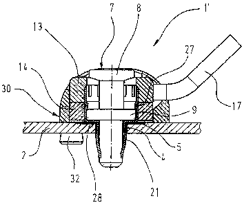
Figure 8 shows a connecting element 1 mounted on a printed circuit board 2
in the form of a cross section. This figure shows the clamping pin 7 that ra-
dially clamps the contact region 21 of the electric contacts 20 against the
inner surface 4 of the opening 3 from inside and thusly produces an electri-
cally conductive connection. The central section 9 formed on the clamping
pin 7 is engaged behind the circumferential constriction 27 in the terminal
CA 02701432 2010-04-27
11
region 22. In this embodiment, the electric contact 20 is encased by two-part
housing 13, 14 that is positioned in the positioning frame 30. The surface 28
of the electric contact 20 is seated on the contact region of the printed
circuit
board 2 in order to enlarge the electric contact area.
CA 02701432 2010-04-27
12
List of Reference Symbols
CONNECTING ELEMENT FOR ELECTRIC CONDUCTORS WITH A
PRINTED CIRCUIT BOARD
File No.: P209-07 CA
1 Connecting element, one-part
1' Connecting element, multipart
2 Printed circuit board
3 Opening
4 Inner surface
Contact area
6
7 Clamping pin
8 Formed-on section, disk-shaped,
9 Central formed-on section, disk-shaped
Housing
11 Opening
12 Formed-on section for electric conductor
13 Housing part, upper
14 Housing part, lower
16 Electric conductor
17 Electric conductor
18
19
Electric contact
21 Contact region
22 Terminal region
23 Bulgy distention
24 Termination
Axial slot
26 Opening, through-opening
27 Constriction
28 Surface, annular contact surface
29 Strip contacts, radially oriented
Positioning frame
31 Recess
32 Encoding pin
33 Receptacle