Note: Descriptions are shown in the official language in which they were submitted.
CA 02701491 2010-03-31
WO 2009/046284 PCT/US2008/078728
FIRMWARE IMAGE UPDATE AND MANAGEMENT
BACKGROUND OF THE INVENTION
Field of the Invention
[0001] The invention generally relates to systems that update and manage
firmware images used by processors.
Background
[0002] Multi-processor systems, such as multi-processor consumer electronics
devices, require a recoverable, foolproof technique for updating processor
firmware without risking that the system will be rendered inoperable. In a
multi-processor system that includes a primary processor and one or more
secondary processors, not only must the system be able to update the firmware
of the secondary processor(s), the system must also have the ability to re-
update the firmware image if the update fails or the system becomes unstable
due to a corruption of the boot image.
[0003] Furthermore, some processors restrict or do not support the ability to
write to program or instruction memory, thereby inhibiting or encumbering the
ability to update the firmware image. For example, some processors only
support updating the firmware image via a special mode of operation in which
the processor reads the new image via a serial port and writes it to flash
memory. Consumer electronics devices that include such processors, such as
some telephone handsets, generally do not support firmware updates. As
device software increases in sophistication, it will be necessary for them to
do
so.
BRIEF SUMMARY OF THE INVENTION
[0004] An embodiment of the present invention allows the firmware of one
processor in a multi-processor system to be updated even if that processor is
unstable due to a corruption of system software. For example, in a system that
CA 02701491 2010-03-31
WO 2009/046284 PCT/US2008/078728
-2-
includes a primary processor and one or more secondary processors, an
embodiment of the present invention allows the firmware of a secondary
processor to be updated even if that processor is unstable due to a corruption
of system software.
[0005] In particular, a method is described herein for updating firmware of a
second processor in a system comprising a first processor and the second
processor. In accordance with the method, the first processor loads a shared
memory with a firmware image. The first processor then sends a command to
the second processor to perform a boot process. Responsive to receiving the
command, the second processor performs a boot process, wherein performing
the boot process includes loading the firmware image from the shared
memory. The foregoing method may further include executing a watchdog
timer mechanism by the first processor, wherein the watchdog timer
mechanism is configured to determine if the second processor has completed
the boot process successfully.
[0006] A system is also described herein. The system includes a first
processor, a second processor, and a shared memory coupled to the first
processor and the second processor. The first processor is configured to load
the shared memory with a firmware image and to send a command to the
second processor to perform a boot process. The second processor is
configured to perform a boot process responsive to receipt of the command,
wherein performing the boot process include loading the firmware image from
the shared memory. The first processor may be further configured to execute
a watchdog timer mechanism, wherein the watchdog timer mechanism is
configured to determine if the second processor has completed the boot
process successfully.
[0007] An embodiment of the present invention also enables a network-based
firmware update of a processor or microcontroller in a system, such as a
consumer electronics device, wherein the processor or microcontroller
requires such updates to occur via a serial port.
CA 02701491 2010-03-31
WO 2009/046284 PCT/US2008/078728
-3-
[0008] In particular, a method is described herein for updating a firmware
image used by a first microcontroller in a system that includes the first
microcontroller and a second microcontroller. In accordance with the method,
the second microcontroller temporarily loads a new firmware image into a
buffer. The second microcontroller then sends a first command to the first
microcontroller. Responsive to receipt of the first command, the first
microcontroller reads the new firmware image from the buffer via a serial port
of the first microcontroller and writes the new firmware image to an
instruction memory associated with the first microcontroller. In loading the
new firmware image into the buffer, the second microcontroller may receive
the new firmware image via a wired network link or a wireless network link.
[0009] The foregoing method may further include sending a message from the
first microcontroller to the second microcontroller to indicate that the first
microcontroller is ready to update the firmware image. The foregoing method
may also include sending a second command from the second microcontroller
to the first microcontroller and responsive to receipt of the second command
by the first microcontroller, resuming a normal execution mode by the first
microcontroller.
[0010] A system is also described herein. The system includes a first
microcontroller, a second microcontroller connected to the first
microcontroller, a buffer connected to the second microcontroller, and an
instruction memory connected to the first microcontroller. The second
microcontroller is configured to temporarily load a new firmware image into
the buffer and to send a first command from the second microcontroller to the
first microcontroller. The first microcontroller is configured to read the new
firmware image from the buffer via a serial port of the first microcontroller
and to write the new firmware image to the instruction memory responsive to
receipt of the first command by the first microcontroller.
[0011] The foregoing system may further include a network link, such as a
wired or wireless network link, and the second microcontroller may be further
configured to acquire the network firmware image via the network link. The
CA 02701491 2010-03-31
WO 2009/046284 PCT/US2008/078728
-4-
first microcontroller may also be further configured to send a message to the
second microcontroller to indicate that the first microcontroller is ready to
update the firmware image. The second microcontroller may also be further
configured to send a second command to the first microcontroller, and the
first
microcontroller may be further configured to resume a normal execution mode
responsive to receipt of the second command.
[0012] Further features and advantages of the invention, as well as the
structure and operation of various embodiments of the invention, are described
in detail below with reference to the accompanying drawings. It is noted that
the invention is not limited to the specific embodiments described herein.
Such embodiments are presented herein for illustrative purposes only.
Additional embodiments will be apparent to persons skilled in the relevant
art(s) based on the teachings contained herein.
BRIEF DESCRIPTION OF THE DRAWINGS/FIGURES
[0013] The accompanying drawings, which are incorporated herein and form
part of the specification, illustrate the present invention and, together with
the
description, further serve to explain the principles of the invention and to
enable a person skilled in the relevant art(s) to make and use the invention.
[0014] FIG. 1 is a block diagram of a multi-processor system that facilitates
the update of firmware in accordance with an embodiment of the present
invention.
[0015] FIG. 2 depicts a flowchart of a method in a system comprising a first
and second processor for updating firmware of the second processor.
[0016] FIG. 3 is a block diagram of a system in which a second
microcontroller is used to load firmware into the instruction memory of a
first
microcontroller via a serial port of the first microcontroller in accordance
with
an embodiment of the present invention.
CA 02701491 2010-03-31
WO 2009/046284 PCT/US2008/078728
-5-
[0017] FIG. 4 depicts a flowchart of a method in a system comprising a first
microcontroller and a second microcontroller for updating a firmware image
used by the first microcontroller.
[0018] The features and advantages of the present invention will become more
apparent from the detailed description set forth below when taken in
conjunction with the drawings, in which like reference characters identify
corresponding elements throughout. In the drawings, like reference numbers
generally indicate identical, functionally similar, and/or structurally
similar
elements. The drawing in which an element first appears is indicated by the
leftmost digit(s) in the corresponding reference number.
DETAILED DESCRIPTION OF THE INVENTION
A. System and Method for Firmware Updates
[0019] As noted in the Background section above, multi-processor systems,
such as multi-processor consumer electronics devices, require a recoverable,
foolproof technique for updating processor firmware without risking that the
system will be rendered inoperable. In a multi-processor system that includes
a primary processor and one or more secondary processors, not only must the
system be able to update the firmware of the secondary processor(s), the
system must also have the ability to re-update the firmware image if the
update fails or the system becomes unstable due to a corruption of the boot
image. An embodiment of the present invention provides a mechanism for
updating the firmware of a secondary processor in such a multi-processor
system even if that processor is unstable due to a corruption of system
software.
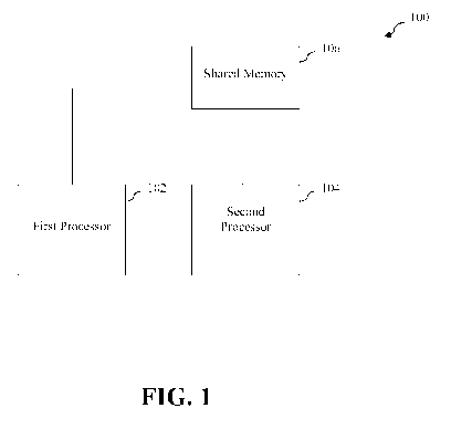
[0020] FIG. 1 is a block diagram of a multi-processor system 100 that
facilitates the update of firmware in accordance with an embodiment of the
present invention. In particular, system 100 allows the firmware of one
processor in system 100 to be updated even if that processor is unstable due
to
a corruption of system software.
CA 02701491 2010-03-31
WO 2009/046284 PCT/US2008/078728
-6-
[0021] As shown in FIG. 1, multi-processor system 100 includes a first
processor 102 and a second processor 104. In an embodiment, first processor
102 comprises a main processor and second processor 104 comprises an
auxiliary processor. First processor 102 and second processor 104 are each
communicatively connected to a shared memory 106, which in an embodiment
comprises a boot memory. Shared memory 106 may comprise a non-volatile
flash memory, although the invention is not so limited.
[0022] Second processor 104 is configured to boot from shared memory 106.
As used herein, the term "boot" means to load and perform a sequence of
operations required to place a processor in its normal operating state. First
processor 102 is configured to populate shared memory 106 with the
appropriate boot code for second processor 104. First processor 102 is further
configured to trigger second processor 104 to initiate a boot. First processor
102 may trigger second processor 104 to initiate the boot by sending one or
more messages via shared memory 106 or by sending one or more messages
over a network or some other communication path between first processor 102
and second processor 104 (not shown in FIG. 1).
[0023] In accordance with an embodiment of the present invention, a
watchdog timer mechanism may be executed by first processor 102 to ensure
that second processor 104 has booted successfully and continues to run. This
watchdog timer mechanism can be implemented in any of several well-known
ways, such as via shared memory 106 or by sending network messages.
[0024] FIG. 2 depicts a flowchart 200 of a method in a multi-processor system
comprising a first and second processor for updating firmware of the second
processor in accordance with the foregoing description. Flowchart 200 will
now be described with continued reference to system 100 of FIG. 1. However,
the method of flowchart 200 is not limited to that implementation.
[0025] As shown in FIG. 2, the method of flowchart 200 begins at step 202 in
which first processor 102 loads shared memory 106 with a firmware image.
At step 204, first processor 102 sends a command to second processor 104 to
perform a boot process. At step 206, responsive to the receipt of the
CA 02701491 2010-03-31
WO 2009/046284 PCT/US2008/078728
-7-
command, second processor 104 performs a boot process, wherein performing
the boot process includes loading the firmware image from shared memory
106.
[0026] In an embodiment, the method of flowchart 200 further includes the
execution of a watchdog timer mechanism by first processor 102, wherein the
watchdog timer mechanism is configured to determine if second processor 104
has completed the boot process successfully.
B. System and Method for Firmware Image Management
[0027] As noted in the Background section above, some processors restrict or
do not support the ability to write to program or instruction memory, thereby
inhibiting or encumbering the ability to update the firmware image. For
example, some processors only support updating the firmware image via a
special mode of operation in which the processor reads the new image via a
serial port and writes it to flash memory. Consumer electronics devices that
include such processors, such as some telephone handsets, generally do not
support such firmware updates. As device software increases in
sophistication, it will be necessary for them to do so.
[0028] An embodiment of the present invention addresses the foregoing
problem by temporarily loading new firmware into a buffer and then using a
secondary microcontroller to set a main microcontroller into update mode
before sending the new firmware to it.
[0029] This approach will now be described with reference to a system
depicted in FIG. 3. In particular, FIG. 3 is a block diagram of a system 300
that includes a first microcontroller 302 and a second microcontroller 304
that
are communicatively connected to each other. In an embodiment, first
microcontroller 302 comprises a main controller and second microcontroller
304 comprises a secondary controller. First microcontroller 302 is
communicatively connected to a first memory 306 and second microcontroller
304 is communicatively connected to a second memory 308. In an
CA 02701491 2010-03-31
WO 2009/046284 PCT/US2008/078728
-8-
embodiment, first memory 306 comprises an instruction memory and second
memory 308 comprises a data memory or buffer.
[0030] System 300 of FIG. 3 provides a mechanism to support a network-
based firmware update by first acquiring a new firmware image into second
memory 308. The new firmware image is acquired by second microcontroller
304 and may be acquired over, for example, a wired or wireless network link.
During this time, first microcontroller 302 is executing in a normal mode.
When first microcontroller 302 is ready to update the firmware, it sends a
signal to second microcontroller 304. Second microcontroller 304 then takes
over, placing first microcontroller 302 into an update mode. During the
update mode, second microcontroller 304 reads data from second memory 308
and writes it into first memory 306 via a serial port of first microcontroller
302. When the update process is complete, second microcontroller 304 then
sends a command to first microcontroller 302 to resume executing in a normal
execution mode.
[0031] FIG. 4 depicts a flowchart 400 of a method in a system comprising a
first microcontroller and a second microcontroller for updating a firmware
image used by the first microcontroller in accordance with the foregoing
description. Flowchart 400 will now be described with continued reference to
system 300 of FIG. 3. However, the method of flowchart 400 is not limited to
that implementation.
[0032] As shown in FIG. 4, the method of flowchart 400 begins at step 402 in
which second microcontroller 304 loads a new firmware image into a buffer,
which is represented by second memory 308 in FIG. 3. Loading the new
firmware image into the buffer may include receiving the new firmware image
via a wired network link or a wireless network link.
[0033] At step 404, second microcontroller 304 sends a first command from to
first microcontroller 302.
[0034] At step 406, responsive to the receipt of the first command, first
microcontroller 302 reads the new firmware image from the buffer via a serial
port and writes the new firmware image to an instruction memory associated
CA 02701491 2010-03-31
WO 2009/046284 PCT/US2008/078728
-9-
with the first microcontroller, which is represented by first memory 306 in
FIG. 3.
[0035] The foregoing method may further include sending a message from
first microcontroller 302 to second microcontroller 304 to indicate that first
microcontroller 302 is ready to update the firmware image.
[0036] The foregoing method may also include sending a second command
from second microcontroller 304 to first microcontroller 302 and, responsive
to receipt of the second command by first microcontroller 302, resuming a
normal execution mode by first microcontroller 302.
C. Conclusion
[0037] While various embodiments of the present invention have been
described above, it should be understood that they have been presented by way
of example only, and not limitation. It will be understood by those skilled in
the relevant art(s) that various changes in form and details may be made to
the
embodiments of the present invention described herein without departing from
the spirit and scope of the invention as defined in the appended claims.
Accordingly, the breadth and scope of the present invention should not be
limited by any of the above-described exemplary embodiments, but should be
defined only in accordance with the following claims and their equivalents.