Note: Descriptions are shown in the official language in which they were submitted.
CA 02701535 2011-02-18
Title of the Invention: PERSONAL DOSIMETER ON THE BASE OF RADIATION
INTEGRATED CIRCUIT
Inventors: Volodymyr POLISHCHUK, Denis SAVOSTIN
References Cited:
PATENT DOCUMENTS
Canadian Patent 1,204,885 5/1986 Ian Thomson
OTHER PUBLICATIONS
B.O'Connell, A.Kelleher, W.Lane, L.Adams, ((Stacked RADFETs for Increased
Radiation
Sensitivity)), IEEE Tran. Nucl. Sci. Vo1.43, N3, June 1996, pp.481-486.
V.Polischuk and G.Sarrabayrouse, ((MOS ionizing radiation dosimeters: from low
to high dose
measurement)), Radiation Physics and Chemistry, Vol.61, 2001, pp.511-513.
G.Sarrabayrouse, D.Buchdahl, V.Polischuk, S.Siskos, ((Stacked MOS ionizing
radiation
dosimeters: potentials and limitations)), Radiation Physics and Chemistry,
Vol.71, 2003,
pp.737-739.
R. H. Crawford, "MOS FET in Circuit Design", New York: McGraw-Hill. 1967.
1
CA 02701535 2011-02-18
THE FIELD OF THE INVENTION
This invention relates to a dosimeter for measuring ionizing radiation and
particularly to
a dosimeter using a Radiation Integrated Circuit (RADIC) as a sensor, which is
based on a
Metal Oxide Semiconductor Field Effect Transistors (MOSFET) and Radiation
Field Effect
Transistors (RADFET), and substantially improves sensitivity in comparison
with existing
RADFET (or insulated gate field effect transistors (IGFET)) and dual RADFET
(or dual
IGFET) dosimeters. The improved radiation sensitivity can be applied in any of
the fields
where radiation dose measurement/ dosimetry is needed and sensitivity is
crucial with respect
to accuracy (e.g. medical therapy, nuclear industry, power plants, etc.)
BACKGROUND OF THE INVENTION
Metal-oxide-semiconductor dosimeters are MOS field-effect transistors with a
specially
processed gate insulator in order to make it radiation soft.
There are presently conventional personnel dosimeters such as thermal
luminescent
devices. Such devices use a small crystal of CaF2 or LiF which traps the
electrons and holes
produced by the ionizing radiation. When heated, light is emitted from the
crystal due to the
emptying of the traps and this light is related to the accumulated dose.
A MOSFET dosimeter as commonly known as a radiation field-effect transistor
(RADFET) measures a shift in the threshold voltage of RADFET caused by
radiation.
Radiation field-effect transistors are their numerous advantages with respect
to thermal
luminescent devices: low cost, small size and weight, robustness, accuracy,
large measurable
dose range, real-time or delayed direct reading, information retention,
possibility of monolithic
integration with other sensors and/or circuitry capable of performing
measurement, signal
conditioning and data processing.
Canadian Pat. No. 1,204,885 which issued May 20, 1986 to Ian Thomson discloses
a
radiation dosimeter comprising a pair of silicon insulated gate field effect
transistors (IGFET)
by measuring the differential threshold between two IGFET sensors exposed to
the same
radiation, in which one is biased into its conducting region, and the other is
biased either off or
to a conducting level less than first. These dual IGFET's dosimeter offer a
sensitivity about 2
mV/cGy for case in which the gate bias is equal to 3 volts, or about 5 mV/cGy
for the case in
which the gate voltage is greater than 10 volts. The temperature sensitivity
of the dual IGFET
sensor has been found to be smaller than 0.1 mV/ C. Over the military
temperature range -
20 C to +50 C, a 70 difference, AVT =7 mV or 1-3 cGy.
The problem associated with this prior art device is that it is not enough
sensitive
dosimeter for use by personnel workers in the medical, nuclear and industrial
field. The
personal dosimeter should have a sensitivity of approximately 0.010 cGy (Rad).
2
CA 02701535 2011-02-18
B.O'Connell, A.Kelleher, W.Lane, L.Adams in a paper entitled <Stacked RADFETs
for
Increased Radiation Sensitivity)) published in IEEE Tran. Nucl. Sci. Vol.43,
N3, June 1996
has demonstrated the radiation sensitivity of 80 mV/cGy by stacking of 15
individual
RADFETs on the same chip.
V.Polischuk and G.Sarrabayrouse in a paper entitled ((MOS ionizing radiation
dosimeters: from low to high dose measurement)) published in the revue of
Radiation Physics
and Chemistry, Vol.61, No 3-6, 2001 presented a stack-connected RADFET
configuration
with RADFETs having a very thick gate oxide of 1,6 pm. To increase the
sensitivity and the
minimum measurable dose up to 14 transistors have been stacked. With this the
output
voltage before irradiation was 18V. A sensitivity as high as 90 mV/cGy has
been obtained.
Both teams claimed about possibility to measure milli-Rad doses. However,
stacked
RADFETs exhibit a number of problems which limit their use in personal
dosimeters. The
problem is that single RADFET has a certain temperature coefficient. The metal
oxide
semiconductor field-effect transistor device has a temperature threshold
voltage dependence
that needs to be accounted for in order that only radiation induced shift in
threshold voltage is
measured by dosimeter. For stacked RADFETs the temperature sensitivity
increases more
than N times (N is number RADFETs in stacked) than single one.
The inventor has measured the temperature sensitivity of stacked RADFETs made
by
B.O'Connell's team by using their RADFETs dosimeters. The temperature response
is 70
mV/ C for 15 MOSFETs in stacked for small constant current mode of 10 pA . If
the reading
temperature is controlled as +/-1 C, the minimum measured dose is about 5 cGy
or 5 Rad.
G.Sarrabayrouse, D.Buchdahl, V.Polischuk, S.Siskos in a paper entitled
((Stacked
MOS ionizing radiation dosimeters: potentials and limitations)) published in
Radiation Physics
and Chemistry, Vol.71, 2003, pp.737-739. proposed to reduce temperature
sensitivity of
stacked RADFETs by measuring stacked RADFETs at the Minimum Temperature
Coefficient
(MTC) point. Indeed this paper presents only the computer simulations. The
temperature
sensitivity at MTC point and threshold voltage drifts were not measured as
well.
Another problem of stacked RADFET is its high output voltage which in some
cases is
about 18 volts. So it is difficult to amplify the small changes of threshold
voltages, caused by
radiation, by using operational amplifiers.
In the present invention in order to increase radiation sensitivity we used
the
amplification principles of MOSFETs inverters described in the book of R. H.
Crawford, "MOS
FET in Circuit Design", New York: McGraw-Hill. 1967.
It is therefore an object of the present invention to provide a radiation
integrated circuit
as a personal dosimeter having a milli-Rad sensitivity and temperature
compensation by
applying amplification principles of inverters.
3
CA 02701535 2011-02-18
SUMMARY OF THE INVENTION
This invention relates to a solid-state dosimeter measuring very low doses of
ionizing
radiation from 0.01 cGy to 2 cGy and more particularly to radiation integrated
circuit (RADIC)
based on RADFET and MOSFET elements or to circuit based on RADFETs and
resistors.
During irradiation of any of RADICs the first RADET (left) in the reference
circuit is biased off
and the second RADFET (right) in the inverter circuit is biased. Thus the
threshold voltage of
the second RADFET varies with the dosage to a considerably greater degree than
that of the
first RADFET. During measurement the threshold voltage change of the second
RADFET
(right) is amplified by its inverter circuit. The output voltage change will
be equal to the
amplified differential threshold voltage change:
Wout=Au*AUT
Thus the present invention solves the problems of low radiation sensitivity of
conventional dual IGFETs and stacked connected RADFETs dosimeters.
Second object of this invention is that this radiation integrated circuit has
minimum
temperature effect and is relatively insensitive to temperature changes. This
is achieved by
measuring the differential threshold voltage from two RADFETs. To assure that
temperature
affect both RADFETs equally the circuits with both RADFET and both MOSFETs or
with two
RADFETs were fabricated in the same silicon substrate, i.e. in the same chip.
The gate oxide
thickness of each RADFET is preferably 1 pm.
BRIEF INTRODUCTION TO THE DRAWINGS
A better understanding of the invention will be obtained by reference to the
detailed
description of the invention below, and to the following drawings, in which:
Figure 1 is a dual IGFET's dosimeter ready for measurement of its differential
threshold
voltage.
Figure 2 is a reading configuration of stacked connected RADFETs dosimeter.
Figure 3 is an inverter with a MOSFET as a load.
Figure 4 is an inverter with a resistor as a load.
Figure 5 is a schematic of the radiation integrated circuit for the basic
embodiment of the
invention in its configuration prepared to accept irradiation.
Figure 6 is a schematic of the radiation integrated circuit dosimeter for the
basic embodiment
of the invention in the reading mode.
Figure 7 is a schematic of the radiation circuit for the second embodiment of
the invention
prepared to accept irradiation.
4
CA 02701535 2011-02-18
Figure 8 is a schematic of the radiation circuit dosimeter for the second
embodiment of the
invention in the reading mode.
Figure 9 shows the response of the radiation circuit as a function of the
radiation dose of
gamma-ray for the second embodiment of the invention.
DETAILED DESCRIPTION OF THE INVENTION
Figure 3 shows an inverter made of two MOSFETs, where T1 is a managing MOSFET
transistor and T2 is a loading MOSFET transistor. Amplification coefficient of
this inverter
according to a prior art from the book of R. H. Crawford referenced in
background of the
invention is
_ I(W/doxL)i
dUout = A f~2
dUin u (W
ldoxL)2
Where (3 is given as
f - oEoxW
doxL
Figure 4 shows an inverter made of a MOSFET and a resistor, where T1 is a
managing
transistor and RD is a loading resistor. Amplification coefficient of this
second inverter
according again to a prior art from the book of R. H. Crawford is proportional
to steepness or
transition conductivity and to the loading resistance:
dUout _ I
Au = -9m * (RD I rd)
dUln
Where (Rollyd) is an equivalent resistance of parallel connected loading
resistor RD and
dynamic drain resistance rd.
R1 * rd
(RlIIrd)=(R1+rd)
9m= r2--fl * lID I
Figure 5 illustrates the basic embodiment of the present invention. The RADFET
Q2
has its gate G2, drain D2 and source S2 connected together and they are
connected to the
common source S. The RADFET Q1 has its gate G1 biased by the battery 4 and its
drain D1
and source S1 are connected to the common source S. Two MOSFETs Q3 and Q4 have
their
drains D3 and D4, gates G3 and G4, sources S3 and S4 connected to the common
source S.
CA 02701535 2011-02-18
Both RADFETS Q1 and Q2 and both MOSFETs Q3 and Q4 are subjected to the same
ionizing radiation. The MOSFETS have thin oxide thickness less or equal than
100 nm and
RADFETs have oxide thickness more or equal than 1 pm. Because the radiation
sensitivity is
proportional to oxide thickness the MOSFET have very small sensitivity in
comparison with
RADFET. It has been found than radiation sensitivity is much greater for the
biased RADFET
Q1 than non-biased RADFET Q2.
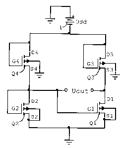
Figure 6 illustrates the basic embodiment of the present invention in the
reading mode.
It shows the same RADFETs Q1 and Q2 and the same MOSFETs Q3 and Q4 in a
radiation
integrated circuit (further RADICI) prepared to measure the radiation dose.
The sources S1
and S2 of the RADFETs are connected together and grounded. The gate G2 of
RADFET Q2
is connected to its own drain D2 and this drain is connected also to the gate
G1 of RADFET
Q1. The gate G3 and the drain D3 of the MOSFETs Q3 are connected together. The
gate G4
and the drain D4 of the MOSFETs Q4 are connected together as well. The source
S3 of
MOSFET Q3 is connected to the drain D1 of the RADFET Q1 and the source S4 of
the
MOSFET Q4 is connected to the drain D2 of the RADFET Q2. A power supply Udd is
connected to the drains D3 and D4 of both MOSFETs. Both MOSFETs should be the
same.
Both RADFETs should be the same as well. Both MOSFETs and both RADFETs are
fabricated in the same die. Thus both RADFETs should have the same temperature
variation
characteristics, the same initial threshold voltage and the same oxide charges
prior to
irradiation. Both MOSFETs should have also the same temperature
characteristics and the
same threshold voltage. The RADFET Q1 and MOSFET Q3 are the inverter which can
amplify the threshold voltage change of RADFET Q1. The amplification of
threshold voltage
change is given by the following equation:
j(W/dOXL)RADFET
Au (W /d0xL)MOSFET
In case when the RADFETs parameters are as W1=1200 pm, L1=50 pm and dox=1
pm and the MOSFET parameters are as W2=20 pm, L2= 2400 pm and dox=0.1 pm the
amplification of threshold voltage change is 17.
The output voltage U.,t is measured between the drains D1 and D2 of the
RADFETs.
Prior to irradiation, the voltage Uoõt is measured as a first amplified
differential threshold. After
irradiation the output voltage Uoõt is measured again. The output voltage
change DU0õt is
equal to the difference between the output voltages before and after
irradiation or to the
amplified differential threshold voltage AUT due to the dosage received:
Wout = Au * LUT
The RADFET Q2 and MOSFET Q4 is the reference circuit which has the same
temperature and drift characteristics as the inverter. Thus the temperature
effect of this
radiation integrated circuit is eliminated.
6
CA 02701535 2011-02-18
Figure 7 illustrates the second embodiment of the present invention. The
RADFET Q6
has its gate G6, drain D6 and source S6 connected together and they are
connected to the
common source S. The RADFET Q5 have its gate G5 biased by the battery 4 and
its drain D5
and source S5 connected to the common source S.
Both RADFETs Q5 and Q6 are subjected to the same ionizing radiation. RADFETs
have oxide thickness equal or more than 1 pm. During irradiation RADFET Q5 is
biased by
the battery 4 and RADFET Q6 is biased off. Thus RADFET Q5 has considerably
higher
radiation sensitivity than RADFET Q6.
Figure 8 illustrates the second embodiment of the present invention in the
reading mode.
Figure 8 illustrates the same RADFETs Q5 and Q6 and the same resistors 2 and 3
in the
radiation integrated circuit 2 (further RADIC2) prepared to measure the
radiation dose. The
sources S5 and S6 of the RADFETs are connected together and grounded. The gate
G6 of
RADFET Q6 is connected to its own drain D6 and this drain is connected also to
the gate G5
of RADFET Q5. The resistor 2 is connected to the drain D5 of the RADFET Q5 and
the
resistor 3 is connected to the drain D6 of the RADFET Q6. A power supply Udd
is connected
to both resistors 2 and 3.
Both RADFETs Q5 and Q6 should be the same and are fabricated in the same die.
Thus both RADFETs should have the same temperature variation characteristics,
the same
initial threshold voltage and the same oxide charges prior to irradiation. The
RADFET Q5 and
resistor 2 are the inverter which can amplify the threshold voltage change of
RADFET Q5.
The amplification of threshold voltage change of RADFET Q5 is given by the
following
equation:
F_ _ lluSoEoxW
Au ( d L )RADFET * I ID I * (R1 I I rd
ox
In case when the RADFETs parameters are such as W=4000 pm, L=40 pm and
R1=1000 k() the amplification of threshold voltage change of the inverter is
15.
The RADFET Q6 and resistor 3 are the reference circuit for the inverter and it
has the
same temperature and drift characteristics as the inverter. Thus the
temperature effect of this
radiation circuit is minimized. The measured temperature sensitivity of RADIC2
is 0.5 mV/C.
The output voltage change DU0õt is equal to the amplified differential
threshold voltage
AUT due to the dosage received (D).
The radiation sensitivity of this radiation circuit (S=MUoõ //D) is 240 mV/cGy
for the case
of biased voltage during irradiation Ubias=3.3V. Taking into account the
measured
temperature sensitivity the minimum measured dose is about 0.01 cGy or 10 mRad
when
temperature is controlled as 1 C .
7
CA 02701535 2011-02-18
Figure 9 shows the experimental output voltage changes as a function of the
irradiation
dose of gamma-rays for radiation integrated circuit (RADIC2).
Thus it may be seen than the radiation integrated circuits (RADIC1 and RADIC2)
of the
present invention provide a more sensitive and accurate dosimeter circuit than
prior art dual
IGFET dosimeter or stacked-connected RADFETs dosimeter.
8