Note: Descriptions are shown in the official language in which they were submitted.
CA 02701905 2010-04-07
WO 2009/052382 PCT/US2008/080314
APPARATUS FOR PERFORMING A STRESS TEST TO ISOLATE AND
MEASURE NOISE IN A PAIRED LINE AND METHOD FOR PERFORMING A
STRESS TEST TO ISOLATE AND MEASURE NOISE IN A PAIRED LINE
This application claims the domestic benefit of United States Provisional
Application Serial No. 60/980,523, filed on October 17, 2007, which disclosure
is
incorporated herein by reference in its entirety.
FIELD OF THE INVENTION
This invention is generally directed to detection of noise in a paired line.
More particularly the present invention relates to an apparatus and method of
measuring noise in a paired telecommunications line. The present invention is
particularly, though not exclusively, an apparatus and method for detecting
and
isolating noise-creating imbalances in a paired line of a telecommunications
cable by
means of a balanced circuit.
BACKGROUND OF THE INVENTION
Paired lines are a conventional means of carrying telecommunications
transmissions. A paired line is made up of two balanced conductors
individually
insulated and twisted together. Paired lines are typically bundled together in
a cable
termed a paired cable, which contains up to one hundred or more paired lines,
wherein
each paired lines is capable of independently carrying telecommunications
signals.
Paired lines are typically effective telecommunications carriers, however, it
is not
uncommon for noise to occur in paired lines which is extremely disruptive to
the
clarity of the transmitted signal.
Test instruments have been developed that contain circuitry suitable to detect
1
CA 02701905 2010-04-07
WO 2009/052382 PCT/US2008/080314
and isolate noise-creating imbalances so that a technician can diagnose the
source of
the problem and eliminate it. This is commonly referred to as the stress test.
United
States Patent Nos. 5,157,336 ("the 1336 patent")and 5,302,905 ("the `905
patent)
disclose circuitry of a test instrument that satisfies this need and their
content is
incorporated herein by reference in their entirety.
A prior art circuit 10 for performing a stress test, such as that described in
the
`905 patent is shown in FIG. 1. The circuit 10 includes a first balanced
outlet pathway
12 in electrical communication with a first conductor of a telecommunications
pair
through a first contact 14, and a second balanced outlet pathway 16 in
electrical
communication with the second conductor of a telecommunications pair through a
second contact 18. An alternating current source 20 provides an alternating
current
signal that is communicated to the first and second conductors through the
first and
second balanced pathways 12, 16 respectively to determine whether the
conductors
are in fact electrically balanced. The circuit 10 also includes a first high
voltage bias
pathway 22 in electrical communication with the first conductor of a
telecommunications pair and a second high voltage bias pathway 24 in
electrical
communication with a second conductor of the telecommunications pair. A direct
current source 26 is connected to the first and second conductors through the
first and
second high voltage bias pathways 22, 24 respectively so that faults that have
been
concealed by galvanic action can be punched through by the DC current and
detected
by the AC signal provided by the alternating current source 20. Measuring
circuitry is
provided by a differential amplifier 21 which detects and measures any
imbalance
between voltage inlet passageways 28, 30.
As shown in FIG. 1 the first balanced outlet pathway 12 includes resistor 32
and capacitor 34 and second balanced outlet pathway 16 includes resistor 36
and
capacitor 38. Capacitors 34, 38 prevent unwanted DC current from damaging the
measuring circuitry 21. In addition capacitors 34, 38 supply the AC current
signal to
the conductors. The AC signal passes through the capacitors 34, 38 a first
time when
the signal is provided to the telecommunications pair and a second time when
the
signal is reflected back from the telecommunications pair and is provided to
the
differential amplifier 21. Because the AC signal, generated by the alternating
current
2
CA 02701905 2010-04-07
WO 2009/052382 PCT/US2008/080314
source 20 and used to perform the stress test, passes through capacitors 34,
38 two
times, any difference between the values of the capacitors 34, 38 is
multiplied and a
false indication of imbalance for the telecommunications pair can result
easily. Thus,
it is important that the capacitors 34, 38 are properly matched.
In order to ensure balance of the first and second pathways 12, 16, a
technician must examine a number of capacitors that have been pre-sorted by
the
manufacturer to locate two capacitors having values within 0.5% of one
another.
After the capacitors have been installed, the capacitors are further matched
to be
within.05% of each other. These steps to match the capacitors are necessary to
ensure that the circuit 10 will operate properly. Because capacitors are
inherently
difficult to manufacture in tight tolerances, the technician can not simply
rely on the
pre-sorted values provided by the manufacturer. Furthermore, because capacitor
values drift with temperature and age, the value of the capacitor may vary
from the
value at the time of manufacture.
,15 It is inefficient, costly, and unreliable to have a technician perform
this vetting
operation. Consequently, there is a need for circuitry that can perform the
necessary
functions of a stress test as described in the `336 and `905 patents in a more
efficient,
economical and reliable manner.
The present invention provides a circuit and method which overcomes the
problems presented in the prior art and which provides additional advantages
over the
prior art, such advantages will become clear upon a reading of the attached
specification in combination with a study of the drawings.
SUMMARY OF THE INVENTION
The present invention provides a circuit and a method of measuring noise in a
paired line which does not require vetting of capacitors to ensure balance
between a
first balanced inlet pathway and a second balanced inlet pathway.
3
CA 02701905 2010-04-07
WO 2009/052382 PCT/US2008/080314
BRIEF DESCRIPTION OF THE DRAWINGS
The organization and manner of the structure and operation of the invention,
together with further objects and advantages thereof, may best be understood
by
reference to the following description, taken in connection with the
accompanying
drawings, wherein like reference numerals identify like elements in which:
FIG. I is a diagram of a prior art circuit for measuring noise in a paired
line;
FIG. 2 is a perspective view of the present invention shown connected to a
schematically depicted telephone system having a paired line; and
FIG. 3 is a diagram of the circuit of the present invention for measuring
noise
in a paired line.
DETAILED DESCRIPTION OF THE ILLUSTRATED EMBODIMENTS
While the invention may be susceptible to embodiment in different forms,
there is shown in the drawings, and herein will be described in detail, a
specific
embodiment with the understanding that the present disclosure is to be
considered an
exemplification of the principles of the invention, and is not intended to
limit the
invention to that as illustrated and described herein.
Referring first to FIG. 2, the noise measuring device of the present invention
is
shown and generally designated 110. As will be described herein below, the
noise
measuring device 110 is used to detect noise in a paired line 30. The paired
line 30
includes first and second conductors 26, 28 which terminate at a central
telephone
office 36. Central telephone offices are generally characterized as having
balanced
input circuits, i.e. balanced impedance to ground. Central office 36 shown in
FIG. 2
is representative of such offices, wherein balanced circuits are provided by a
first
terminal 38 having a resistor 40 and a second terminal 42 having an equal
resistor 44.
Terminal 42 further has a direct current battery 46 in series. Both terminals
38 and
42 lead to ground 47. Battery 46 supplies the operating current to the
telephone loop
which is defined by paired line 30.
A series resistance fault 48 is shown on second conductor 28 which creates an
imbalance in paired line 30 between first and second conductor 26, 28. It is
understood that fault 48 is illustrative of any number of sources of imbalance
in paired
4
CA 02701905 2010-04-07
WO 2009/052382 PCT/US2008/080314
line 30 to which the present invention is applicable, including shunt
resistance faults,
cross faults, shunt capacitance faults, unbalanced series inductance, and
power
influence.
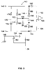
The internal circuit of the device 110 is shown in FIG. 3 and is contained
within the housing 112. A display 114, such as a liquid crystal display, is
provided
through housing 112 for visually displaying measured noise or balance values
to an
operator. First measuring lead 116, second measuring lead 118, and ground lead
120
extend from housing 112. First measuring lead 116 includes a first contact 122
affixed on an end thereof, second measuring lead 118 includes a second contact
124
affixed on an end thereof, and ground lead 120 has a ground contact 132
affixed on an
end thereof. First contact 122 is removably engagable with the first conductor
26,
second contact 124 is removably engagable with the second conductor 28 and
ground
contact 132 is removably engagable with an earth ground 134. Contacts 122,
124,
132 are preferably conventional alligator clips which are toothed and spring
biased to
made good electrical contact upon engagement with conductors 26, 28 or ground
34
and yet are easily removable for repositioning.
Referring now to FIG. 3, a preferred embodiment of the internal circuit of
device 110 is shown and generally designated 140. The internal circuit 140 is
substantially the same as the prior art circuit 10 shown in FIG. 1.
The circuit 140 includes a first contact 142, a second contact 144, and a
third
contact 146. The first contact 42 provides external connection to the first
conductor
26 of the paired line 30 through contact 122 and lead 116, the second contact
144
provides external connection to the second conductor 28 of the paired lines 30
through
contact 124 and lead 118, and the third contact 146 provides external
connection to
the earth ground 34 through contact 32 and lead 120,
As also shown in FIG. 3 the internal circuit 140 generally includes a ground
pathway 156, a first balanced outlet pathway 148, a second balanced outlet
pathway
150, a first high voltage bias pathway 180, a second high voltage bias pathway
182, a
terminating pathway 170, a first voltage inlet pathway 152, and a second
voltage inlet
pathway 154. A node 158 provides connection of the internal circuit 140 to
earth
ground.
5
CA 02701905 2010-04-07
WO 2009/052382 PCT/US2008/080314
The ground pathway 156 generally includes an oscillator 160, a dc power
source 162 and an ac blocking capacitor 196. The ac blocking capacitor 196
prevents
the ground pathway 156 from drawing ac power influence current to ground to
undesirably seal fault 48. In addition, capacitor 196 minimizes low frequency
ac
power influence current and the dc loop current drawn by the ground pathway
156.
The oscillator 160 provides a low voltage alternating current source feeding
into
conductors 26, 28 across the first and second balanced outlet pathways 148,
150. Low
voltage ac is defined herein as preferably being less than about 10 volts.
First balanced outlet pathway 148 extends from earth ground 158 to the first
conductor 26 through the first contact 142. The first balanced outlet pathway
148
includes a first balanced capacitor 184 and a first balanced resistor 186.
Capacitor
184 preferably has a value of 2.2 F and resistor 186 preferably has a value of
1 KQ.
Second balanced outlet pathway 150 extends from earth ground 158 to second
conductor 28 through the second contact 144. The second balanced outlet
pathway
includes a second balanced capacitor 188 and a second balanced resistor 190.
Capacitors 184, 188 are matched within .5%. Capacitor 188 preferably has the
same
value as capacitor 184 and thus preferably has a value of 2.2 F. Resistorl90
preferably has the same value as resistor 186 and thus preferably has a value
of I K.
The first high voltage bias pathway 172 extends from earth ground 158 to the
first conductor 26 through the first contact 142. The first high voltage bias
pathway
includes a high value resistor 180 which preferably has a value of I OOKQ.
Second
high voltage bias pathway 174 extends from earth ground 158 to the second
conductor
28 through second contact 144. The second high voltage bias pathway includes a
high value resistor 182 which preferably has the same value as resistor 180.
Terminating pathway 170 is provided between first contact 142 second contact
144. Terminating pathway 170 includes a dc isolating capacitor 176 in series
with a
line terminating resistor 178.
The first voltage inlet pathway 152 extends from contact 142 to a first input
of
a differential amplifier 168. The first voltage inlet pathway includes a
capacitor 192.
The second voltage inlet pathway 154 extends from contact 144 to a second
input of
the differential amplifier 168 and includes a capacitor 194. Capacitors 192,
194 are
6
CA 02701905 2010-04-07
WO 2009/052382 PCT/US2008/080314
matched within 5%. The differential amplifier 168 of the present invention
provides
measuring means in electrical communication with the first and second voltage
inlet
pathways 152, 154.
The circuit 140 of the present invention operates in the following manner. In
the same manner as the circuit 10 of FIG. 1, the circuit 140 is attached to
the first and
second conductors 26, 28 of the telecommunications line 30 and to earth ground
34
using contacts 122, 124 and 132 respectively. AC signals and high voltage DC
is
placed on the metal insulation of the telecommunications pair 30 using
oscillator 160,
DC power source 162, and capacitor 196. The AC signal is coupled to conductors
26,
28, corresponding to ring and tip of the telecommunication pair. The AC signal
is
loaded to ground 34 through connection 146 by the first and second balanced
output
pathways 148, 150. Resistors 186 and 190 as well as capacitors 184, 188, must
be
balanced to a variance less than the smallest desired value of measurement by
the
circuit 140. At the same time, DC current supplied by DC power source 162 is
1.5 provided to the first and second high voltage bias pathways 172, 174 to
break down
any high impedance faults and allows the AC signal to pass through the ring or
tip
conductors, revealing the fault.
The AC signal is reflected back to the stress test circuit 140 through
contacts
.142, 144 while resistor 178 and capacitor 176 filter out unwanted noise.
Then, the AC
signal passes through isolation capacitors 192 and 194 to the differential
amplifier
168. The differential amplifier 168 receives metallic voltage signals from
voltage inlet
pathways 152, 154 and measures the voltage difference. Any difference of the
capacitance between the two conductors 26, 28., will cause amplitude and phase
changes of the coupled tone which is measured by the differential amplifier
168. The
device 110 provides similar stress test results when using standard testing
protocols
under similar circumstances as devices employing the circuit 10 shown in FIG.
1. Any
amplitude or phase changes of the coupled tone measured by the differential
amplifier
168 are converted to a corresponding expression of noise or balance and fed to
display
114. A log amplifier (not shown) may be provided for converting the voltage
difference from amplifier 168 to a measure of noise in decibels, typically in
units of
decibels reference noise (dBrn), or a measure of balance also in decibels. The
DC
7
CA 02701905 2010-04-07
WO 2009/052382 PCT/US2008/080314
current is also reflected back into the stress test circuit 140 through
connections 142
and 144 to ground 158 through resistors 180 and 182.
Thus, circuit 140 performs a stress test similar to that performed by the
circuit
of FIG. 1, however, the circuit 140 eliminates the need for a technician to
vet
5 capacitors so that the circuit 140 will operate properly. As shown in FIG. 1
the first
voltage inlet pathway 28 extends from first contact 14 to a first input of the
differential amplifier 21 and includes a first balanced capacitor 34. The
second voltage
inlet pathway extends from second contact 18 to a second input of the
differential
amplifier 21. In the circuit 10, the AC signal is applied to the first and
second
10 balanced outlet pathways at node 35 and is passed to conductors 26, 28 of
the
telecommunications pair 30 through balanced resistors 32, 36 and balanced
capacitors
34, 3 8. The AC signal is reflected back to the stress test circuit 10 through
the
contacts 14, 18 and the balanced capacitors 34, 38 to the first and second
inputs of the
differential amplifier 21. Thus, any returnAC signals from the first and
second
conductors 26, 28 of a telecommunications pair 30 is passed through the
capacitors
34, 38 before reaching the differential amplifier 21. Asa result, capacitors
34, 38 of
the circuit 10 are required to be matched within .05% as described above. In
contrast
the circuit 140 of the present invention shown in FIG. 3, provides for
relocation of the
first and second voltage inlet pathways 152, 154, such that they are now
connected to
what would have been nodes 33, 37 of the circuit 10. Hence, capacitors 184,
188
only function to apply the desired AC signal onto the first and second
conductors 26,
28 of the paired telecommunications line 30 and do not also serve to isolate
the
differential amplifier 168 and other components of the measurement circuitry
from
damage from DC current because the measurement of the AC signals as they
return
from the conductors 26, 28 of the telecommunications line 30 is taken before
the AC
signals reach capacitors 184, 188 a second time. Thus, only capacitors with
values of
2.2 microfarads and a tolerance of .5% are required. -Because manufacturing
tolerances provide that capacitors marked with equal values will be matched
within
.5%, the need for vetting of capacitors is eliminated.
A need still exists to protect the measurement circuitry 168 from high voltage
DC current in the circuit 140. Consequently, new capacitors 192, 194 have been
8
CA 02701905 2010-04-07
WO 2009/052382 PCT/US2008/080314
included with values of only I microfarad and lose tolerances to prevent DC
current
from reaching the measurement circuitry 168 of the test instrument 110. Only
capacitors of low values and tolerances are required because the impedance of
the
measurement circuit is very high. Furthermore, the load and isolation tasks of
the
original capacitors 34, 38 of the circuit 10 shown in FIG. 1 have been split
by adding
additional capacitors. In the circuit 140, the load task is performed by
capacitors 184,
188 and the isolation task is performed by capacitors 192, 194. Thus, the
tolerance
requirements for the capacitors of the circuit 140 are redistributed among
more
components.
Each balanced outlet pathway 148, 150 includes a capacitor 184, 188 in series
with a resistor 186, 190. Although the capacitors 184, 188 are positioned
proximate
the earth ground 34 in the circuit 140, it is to be understood that the
positions of the
capacitors 184, 188 and the resistors 186, 190 could be swapped such that the
resistors
186, 190 are positioned proximate the node 158. However, by providing the
capacitors 184,188 connected directly to earth ground 158 as shown in FIG. 3,
capacitors 184, 188 can be varied by simply adding or removing parallel
capacitance
with a transistor to ground. This enables the circuit 140 to auto-calibrate
efficiently if
so desired, allowing capacitors 184 and 188 to vary as much as 10% in value
without
fear of ruining the quality of measurement by the stress test circuit 140.
As can be seen, this invention provides a more efficient way of performing the
stress test because it does not require a technician to vet capacitors. In
addition,
because the need to vet capacitors is eliminated, the circuit 140 is less
prone to human
error and therefore is more reliable. Finally, the amount of time required to
assemble
the circuit is reduced which results in reduced labor cost, making this
circuit 140 more
economical than the previous stress test circuits.
While preferred embodiments of the present invention are shown and
described, it is envisioned that those skilled in the art may devise various
modifications of the present invention without departing from the spirit and
scope of
the appended claims.
9