Note: Descriptions are shown in the official language in which they were submitted.
CA 02702436 2010-04-12
WO 2009/052329 PCT/US2008/080230
LIGHT EMITTING DEVICE WITH PHOSPHOR WAVELENGTH CONVERSION
CLAIM OF PRIORITY
U.S. Patent Application No. 11/975.130 entitled LIGHT EMITTING DEVICE WITH
PHOSPHOR WAVELENGTH CONVERSION, by Yi-Qun Li, filed October 17, 2007 (Attorney
Docket No. ITMX-00225US0).
BACKGROUND OF THE INVENTION
Field of the invention
The invention relates to light emitting devices with phosphor wavelength
conversion.
More specifically, the present embodiments are directed to light emitting
diode based lighting
systems with phosphor, photo-luminescent, wavelength conversion to generate a
desired
color and/or color temperature of light.
Description of the Related Art
The development of solid state semiconductor devices, in particular light
emitting
diodes (LEDs), has opened up the possibility of a new generation of energy
efficient lighting
systems. it was not until LEDs emitting in the blue/ultraviolet part of the
electromagnetic
spectrum were developed that it became practical to develop white light
sources based on
LEDs ("white LEDs").
As taught for example in US 5,998,925, white LEDs include one or more phosphor
materials, that is photo-luminescent materials, which absorb a portion of the
radiation emitted
by the LED chip and re-emit light of a different color (wavelength).
Typically, the LED chip or
die generates blue light and the phosphor(s) absorb a percentage of the blue
light and re-
emit yellow light or a combination of green and red light, green and yellow
light or yellow and
red light. The portion of the blue light generated by the LED that is not
absorbed by the
phosphor (that is the portion transmitted by the phosphor) is combined with
the light emitted
by the phosphor and provides light which appears to the human eye as being
nearly white in
color. Phosphor layers are typically placed, for example, adjacent or in close
proximity to a
light emitting surface of the LED die/chip from which they derive their
excitation energy.
Often, the phosphor layer is coated directly onto the LED die to achieve the
desired intensity
and color of illumination product.
As is known, the correlated color temperature (COT) of a white light source is
determined by comparing its hue with a theoretical, heated black-body
radiator. OCT is
specified in Kelvin (K) and corresponds to the temperature of the black-body
radiator which
radiates the same hue of white light as the light source. The GOT of a white
LED is generally
determined by the phosphor composition and the quantity of phosphor
incorporated in the
1
CA 02702436 2010-04-12
WO 2009/052329 PCT/US2008/080230
LED.
Today, most lighting fixture designs utilizing LEDs comprise systems in which
an LED
(more typically an LED array to achieve a desired intensity of generated
light) replaces
conventional system components such as incandescent bulbs, mercury vapor and
compact
fluorescent lamps. In the case of lighting systems intended to generate a
white light
illumination product, the LEDs can comprise an array of red, green and blue
direct light
generating LEDs (that is LEDs without the inclusion of a wavelength converting
phosphor
material) or more recently an array of white LEDs.
As disclosed in US 6,350,041, WO 2004/160226 and our co-pending US patent
applications 11/627,390 and 111714,464, the phosphor material can be provided
remotely
from its associated excitation source.
US 6,350,041 teaches a solid state lamp based on an LED which emits radially
dispersed light for room illumination and other applications. The lamp
comprises a solid state
light source such as an LED or laser which transmits light through a separator
to a disperser
that disperses the light in a desired pattern and/or changes the color of
light. In one
embodiment, the light source comprises a blue light emitting LED, the
separator is a light
pipe or fiber optic device and the disperser disperses the light radially and
converts some of
the blue light to yellow to produce a white light illumination product. The
separator spaces the
LED a sufficient distance from the disperser such that heat from the LED will
not transfer to
the disperser when the LED is operated at elevated currents as is necessary
for room
illumination. Such a lamp can disperse light in many patterns, but is
particularly applicable to
a radial dispersion of white light for room illumination enabling the lamp to
be used as an
alternative light source in existing luminaires and lighting fixtures.
Our co-pending US patent application, serial number 11/827,890 filed July 13,
2007;
teaches LED lighting/illumination systems/fixtures or luminaires in which the
phosphor
material is located remotely from its associated excitation source (LED).
Light generated by
the LED is transported to the phosphor material via a waveguiding medium and
provides
excitation radiation to the phosphor(s) and/or phosphor layers), causing a
photo
luminescence. The light from the phosphor(s) may comprise the final
illumination product, or
it may be combined with any visible light from the excitation source (which
may occur, for
example, in the case of a blue LED as the excitation source). The final
illumination product
may be white light, or any colored light. The waveguide can be configured to
be in the shape
of a lighting system such as a hanging lighting fixture, a desk lighting
fixture, a floor standing
lighting fixture, a desk lamp, track lighting, spot lighting, accent lighting
or a lighting panel for
incorporation into a suspended ceiling, in the lighting panel configuration,
the waveguide is
substantially planar in form and has the phosphor provided over the entire
light emitting face
of the waveguide. Excitation radiation generated by a plurality of LEDs is
coupled into one or
2
CA 02702436 2010-04-12
WO 2009/052329 PCT/US2008/080230
more edges of the waveguide such as to propagate substantially throughout the
waveguide
and is then emitted through the light emitting face where at least a part of
the excitation
radiation excites the phosphor which emits light of a second wavelength. To
prevent light
being lost through the rear face of the panel a reflecting layer is provided
on the rear face of
the waveguide, that is the face opposite the light emitting face.
US patent application serial number 11/714,464 filed May 3, 2007, teaches
lighting
fixtures and systems in which the phosphor is provided on a shade which is
located remotely
from the excitation source (LED). The shade (optical enclosure) is configured
to at least in
part surround the LED such that excitation radiation travels, propagates in
freespace (that is,
1,0 it is not guided by an optical medium), a distance of at least one
centimeter from the
excitation source to the shade. The phosphor can be provided on the inner
surface or outer
surface of the shade or incorporated within the shade material. In one
embodiment the
lighting system comprises a bulkhead light which comprises a housing
containing one or
more LEDs and the shade comprises a front window covering the housing opening.
The
housing which is made of an opaque material includes reflective inner surfaces
for reflecting
light towards the shade.
VVO 2004/100226 discloses an LED panel lamp comprising an enclosure housing a
plurality of UV emitting LEDs and a removable front light emitting panel
containing one or
more UV excitable phosphor materials. Since a phosphor material generates
light that is
radiated equally in all directions (isotropic), some of the phosphor generated
light will be
directed backwards into the enclosure. To prevent such light entering the
enclosure and
being lost, the front panel includes a coating on its interior surface which
is transmissive to
the wavelengths of the LED yet reflective to wavelengths produced by the
phosphor(s).
Moreover, to prevent bleed through of non-converted UV light, the front panel
can include a
second coating on its exterior surface which is reflective to UV light and
transmissive to the
light generated by the phosphor(s). The document also describes a lighting
system which
resembles a standard incandescent light bulb in which one or more phosphor
materials are
included on the inner surface of the bulb envelope.
While such lighting system designs may have demonstrated properties that are
acceptable to some customers - properties such as intensity, color temperature
and color
perception, for instance - a need exists for a lighting system based on solid-
state
components of even higher efficiency.
SUMMARY OF THE INVENTION
3 The present invention arose in an endeavor to provide a light emitting
device with
phosphor wavelength conversion which, at least in part, overcomes the
limitations of the
known devices. Embodiments of the present invention are directed to light
emitting devices
3
CA 02702436 2010-04-12
WO 2009/052329 PCT/US2008/080230
comprising an excitation source, which may for example be an LED or a laser
diode, and a
light emitting surface that includes one or more phosphor, photo luminescent,
materials. Light
from the excitation source provides an excitation radiation to the phosphor(s)
causing a
photo luminescence. The light generated by the phosphor combined with light
from the
excitation source comprises the illumination product of the device. In
contrast to the known
devices the light emitting area further comprises one or more areas
(window(s)) which do not
include phosphor material and which are substantially transparent to both
light generated by
the phosphor and by the excitation source, Such windows improve the efficiency
of the
device by maximizing light emitted by the device.
According to the invention a light emitting device comprises: at least one
excitation
source, such as one or more blue light emitting diodes, which is/are operable
to generate
excitation light of a first wavelength range and a light emitting surface
having at least one
phosphor material which absorbs at least a part of the excitation light and
emits light of a
second wavelength range, wherein light emitted by the device comprises
combined light of
the first and second wavelength ranges emitted by the light emitting surface,
characterized in
that the light emitting surface has at least one window area which does not
include the at
least one phosphor material, said window area being substantially transparent
to light of the
first and second wavelengths.
The light emitting surface preferably comprises a transparent substrate, such
as an
acrylic, polycarbonate, polythene or glass material, which is substantially
transparent to light
of the first and second wavelengths and which has the at least one phosphor
material on a
surface thereof. The phosphor material can comprise an array (pattern) of
phosphor regions
(islands) in which the gaps between phosphor regions defines the at least one
window area.
To ensure a uniform color and/or color temperature of emitted light the
pattern of phosphor
regions is distributed, preferably substantially uniformly, over substantially
the entire area of
the light emitting surface. In one such an arrangement, in which the array of
phosphor
regions comprises a regular array of square phosphor regions, the window area
will be grid-
like in form and is distributed over the light emitting surface. The phosphor
regions can, for
example, be substantially polygonal, square, circular, elliptical, triangular
or rectangular in
shape. Conversely, the phosphor material can cover the entire light emitting
surface and
include an array of window areas. To ensure a uniform color and/or color
temperature of
emitted light the pattern of window areas regions is distributed, preferably
substantially
uniformly, over substantially the entire area of the light emitting surface.
As with the phosphor
regions the window areas can, for example, be substantially polygonal, square,
circular,
elliptical, triangular or rectangular in shape. The array of phosphor regions
and/or window
areas can be a regular or irregular pattern.
The substrate can be configured as an optical component through which the
4
CA 02702436 2010-04-12
WO 2009/052329 PCT/US2008/080230
excitation light and phosphor generated light passes. Alternatively, the
substrate can be
configured as a waveguiding (light-guiding) medium and the excitation source
configured to
couple excitation light into the substrate. in one such arrangement the
substrate is
substantially planar in form and the excitation light is coupled into at least
a part of one edge
of the substrate. Preferably, the device further comprises a reflector on at
least a part of the
surface of the substrate opposite to the light emitting surface to help ensure
that substantially
all light is emitted from the light emitting surface. To promote the emission
of light from the
light emitting surface, the light emitting surface of the substrate can
include a surface
topology, such as a surface patterning. The surface topology can be 5 defined
by laser or
1,0 mechanical scribing the substrate surface, molding the substrate to
include the surface
topology or roughening the surface The substrate can comprise other waveguide
forms such
as being elongate or cylindrical in form, with the light emitting surface
being a substantially
flat face or curved surface of the waveguide.
Where it is required to generate light of a particular color and/or CCT, the
light
emitting surface preferably comprises a pattern of at least two different
phosphor materials.
The phosphor compositions, density of phosphor material and the relative total
areas of the
phosphor materials and window area(s) can be used to control the color and/or
CCT of the
emitted light.
For a light emitting device which is intended to generate white light with a
high CRl
(color rendering index), the device can further comprise one or more LEDs
which is/are
operable to generate light of a third wavelength range which contributes to
light emitted by
the device by the light emitting surface. in one arrangement, blue LEDs are
used to excite a
green emitting phosphor material and orange or red LEDs used to generate
orange or red
light components of the final emission product. it will be appreciated that in
such an
arrangement the emission product comprises red (R), green (G) and blue (B)
color
components. Preferably, the ratio of blue LEDs to orange or red LED chips is
substantially
two-to-one to ensure that the green light contribution is sufficient to
achieve a required CRI.
It will be appreciated that in such an arrangement light generated by the
orange or red LEDs
does not result in excitation of the phosphor and such light is emitted
through the one or
more window areas in the light emitting phosphor surface. In an alternative
arrangement blue
LEDs can be used to excite an orange or red emitting phosphor and one or more
green
emitting LED chips used to contribute green light to the emission product.
The phosphor material can comprise. a silicate-based phosphor; an aluminate-
based
phosphor; a nitride-based phosphor material; a sulfate-based phosphor
material; an oxy
nitride-based phosphor; an oxy-sulfate-based phosphor; a garnet material; a
silicate-based
phosphor of a general composition A3Si(OD)s in which Si is silicon, 0 is
oxygen, A comprises
strontium (Sr), barium (Ba), magnesium (Mg) or calcium (Ca) and D comprises
chlorine (Cl),
5
CA 02702436 2010-04-12
WO 2009/052329 PCT/US2008/080230
fluorine (F), nitrogen (N) or sulfur (S); a silicate-based phosphor 5 of a
general composition
A22Si(OD)4 in which A comprises Sr, Ba, Mg or Ca and D comprises Cl, F, N or
S; or an
aluminate-based phosphor of formula M,_YEu,AI,,0jj, a,r2l in which M is at
least one of a
divalent metal comprising Ba, Sr, Ca, Mg, Mn, Zn, Cu, Cd, Sm or thulium (Tm),
According to a further aspect of the invention a light emitting device
comprises: an
enclosure having a reflecting inner surface; at least one excitation source
housed within the
enclosure and operable to generate excitation light of a first wavelength
range; and a light
emitting surface covering the opening of the enclosure and having at least one
phosphor
material which absorbs at least a part of the excitation light and emits light
of a second
1,0 wavelength range, wherein light emitted by the device comprises combined
light of the first
and second wavelength ranges emitted by the light emitting surface,
characterized in that the
light emitting surface has at least one area which does not include the at
least one phosphor
material, said area being substantially transparent to light of the first and
second
wavelengths thereby allowing a part of excitation light and reflected phosphor
generated
light to pass through the light emitting surface.
BRIEF DESCRIPTION OF THE DRAWINGS
In order that the present invention is better understood embodiments of the
invention
will now be described, by way of example only, with reference to the
accompanying drawings
in which:
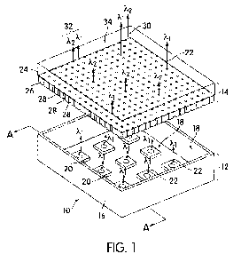
Figure 1 is a partially exploded perspective schematic representation of a
backlit lighting
panel in accordance with the invention;
Figure 2 is a schematic cross sectional representation of the backlit lighting
panel of Figure 1
through a plane AA;
Figure 3 is a light emitting phosphor panel in accordance with the invention
for use in the
lighting panel of Figures 1 and 2;
Figures 4a and 4b are light emitting phosphor panels in accordance with
further
embodiments of the invention,,
Figure 5 is a partially exploded perspective schematic representation of an
edge-lit lighting
panel in accordance with the invention;
Figure 6a is a schematic cross sectional representation of the edge-lit
lighting panel of Figure
5;
Figure 6b is a schematic cross sectional representation of an edge-lit
lighting panel in
accordance with a further aspect of the invention;
3 5 Figure 7 is a partial cut-away perspective representation of a reflector
lamp in accordance
with the invention;
Figure 8 is a partial cut-away perspective representation of a light bulb in
accordance with
6
CA 02702436 2010-04-12
WO 2009/052329 PCT/US2008/080230
the invention; and
Figure 9 is a partial cut-away perspective schematic representation of a
tubular lamp in
accordance with the invention.
DETAILED DESCRIPTION OF THE INVENTION
Figures 1 and 2 are respectively perspective and cross sectional schematic
representations of a white light emitting lighting panel 10 in accordance with
the invention.
The lighting panel 10 is intended for use in a suspended (drop) ceiling of a
type commonly
used in offices and commercial premises in which a grid of support members (T
bars) are
suspended from the ceiling by cables and ceiling tiles/lighting panels are
supported by the
grid of support members. Typically, the ceiling tiles are square (2 feet x 2
feet, 60cm x 60cm)
or rectangular (4 feet x 2 feet, 12 cm x 60cm) in shape and the lighting panel
of the invention
is configured to fit within such an aperture.
The lighting panel 10 comprises a backlighting unit 12 and a light emitting
phosphor
panel 14. The backlighting unit 12 comprises a light box 16 which is
fabricated from, for
example, sheet metal, molded from a plastics material or constructed from any
other suitable
material. To maximize light emission from the lighting panel, the inner
surfaces 18 of the light
box 16 preferably comprise light reflecting surfaces to reflect light towards
the light emitting
panel 14. An array of light emitting diodes (LEDs) 20 is provided within the
light box 16. Each
LED 20 is operable to generate light 22 of wavelength k and each preferably
comprises an
InGaN/GaN (indium gallium nitride/gallium nitride) based LED chip which
generates blue light
of wavelength 400 to 480nm. A square array of nine LED chips 20 is illustrated
though it will
be appreciated that the number and layout of the LEDs can be modified to suit
a required
application. As will be described the light 22 generated by the LEDs 20
provides two
functions; firstly it comprises a part of the final illumination product 32
and secondly it
provides excitation radiation for exciting the phosphor material of the
phosphor panel 14. In
view of the latter function the light 22 will hereinafter be referred to as
excitation light.
The light emitting phosphor panel 14 comprises a transparent substrate 24,
such as
for example an acrylic sheet, having a layer of phosphor material (photo-
luminescent
material) 2, provided on an under surface, that is the surface of the
substrate facing the
LEDs. In other arrangements the transparent substrate 24 can comprise other
transparent
materials such as for example a polycarbonate, polythene, or glass. The
phosphor material
26 can comprise any photo-luminescent material which is capable of being
excited by the
excitation light 22 such as for example, silicate, ortho-siliÃcate, nitride,
oxy-nitride, sulfate,
oxy-sulfate, garnet or aluminate based phosphor materials. In preferred
embodiments the
phosphor material is a silicate-based phosphor of a general composition
A3Si(OD)5 or
A2Si(OD)4 in which Si is silicon, 0 is oxygen, A comprises strontium (Sr),
barium (Ba),
7
CA 02702436 2010-04-12
WO 2009/052329 PCT/US2008/080230
magnesium (Mg) or calcium (Ca) and 0 comprises chlorine (C), fluorine (F),
nitrogen (N) or
sulfur (S). Examples of silicate-based phosphors are disclosed in our co-
pending 30 patent
applications US2006/0145123, US20061028122, US2 061 61309, U x 0 70 9 6 and
111786,044, filed April 9, 2007 the content of each of which is hereby
incorporated by way of
reference thereto.
As taught in US200610145123, a europium ( u") activated silicate-based green
phosphor has the general formula (Sr,A1),(Si,.A2)(0,A3)2+,:Eu2 in which: A-,
is at least one of a
2+ cation, a combination of 1+ and 3+ cations such as for example Mg, Ca, Bar
zinc (2:n),
sodium (Na), lithium (Li), bismuth (Bi), yttrium (Y) or cerium (Ce); A2 is a
3+, 4+ or 5+ cation
1,0 such as for example boron (B), aluminum (Al), gallium (Ga), carbon (C),
germanium (Ge), N
or phosphorus (F);; and .A3 is a 1-, 2- or 3- anion such as for example F, Cl,
bromine (Br), N or
S. The formula is written to indicate that the A, cation replaces Sr; the Aa
cation replaces Si
and the A;3 anion replaces Q. The value of x is an integer or non-integer
between 2.5 and 3.5.
US2006/028122 discloses a silicate-based yellow-green phosphor having a
formula
A2SiQ4:Bu24 D, where A is at least one of a divalent metal comprising Sr, Ca,
Bar Mg, Zn or
cadmium (Cd) and D is a dopant comprising F, Cl, Br, iodine (I), P; S and N.
The dopant D
can be present in the phosphor in an amount ranging from about 0.01 to 20 mole
percent.
The phosphor can comprise (Sr1.x.,.Ba~MY) SiO4:Bu2 F in which M comprises Ca,
Mg, Z n or
Cd.
U52006/261309 teaches a two phase silicate-based phosphor having a first phase
with a crystal structure substantially the same as that of (Ml)?Si04; and a
second phase with a
crystal structure substantially the same as that of (M2)3SiO5 in which MI and
M2 each
comprise Sr, Ba, Mg, Ca or Zn. At least one phase is activated with divalent
europium (Eu2 )
and at least one of the phases contains a dopant D comprising F, Cl, Br; S or
N. it is
believed that at least some of the dopant atoms are located on oxygen atom
lattice sites of
the host silicate crystal.
US2007/029526 discloses a silicate-based orange phosphor having the formula
(Sr3.
,Mx)yBu,SiOs in which M is at least one of a divalent metal comprising Ba, Mg,
Ca or Zn;
O<x<0.5; 2.6<y<3.3; and 0.001<z<0.5. The phosphor is configured to emit
visible light having
3o a peak emission wavelength greater than about 565 nm.
11/786,044 teaches an orange-red phosphor of general formula (A1A2)3(S
B,)(QCq)5
in which A and Aa each comprise Sr, Bar Mg, Ca, Zn, Y, lanthanum (La),
praseodymium
(Pr); samarium (Sm) or Bi, B., comprises Al, B, P or Ge and C, comprises F,
Cl, Br, S or N.
The phosphor can also comprise an aluminate-based material such as is taught
in our
:>s copending patent applications US2006/0158090 and US2006/0027786 the
content of each of
which is hereby incorporated by way of reference thereto.
US200610158090 teaches an aluminate-based green phosphor of formula M3.
8
CA 02702436 2010-04-12
WO 2009/052329 PCT/US2008/080230
YEu AlY31q .,3.,2.1 in which M is at least one of a divalent metal comprising
Ba, Sr, Ca, Mg; Mn,
Zn, Cu, Cd, Sm and thulium (Tm) and in which 0,1<x<0.9 and 0.5 <y s12.
US200610027786 discloses an aluminate-based phosphor having the formula (M.
,,Eua),, ;;1' g,A1,C?[, ,,,.vl in which M is at least one of a divalent metal
of Ba or Sr. In one
composition the phosphor is configured to absorb radiation in a wavelength
ranging from
about 280 nm to 420 nm, and to emit visible Tight having a wavelength ranging
from about
420 nm to 560 nm and 0.05<x<0.5 or 0.2<_x<0.5; 3 y s12 and 0.8 Sa X12. The
phosphor can
be further doped with a halogen dopant H such as Cl, Br or I and be of general
composition
( ~-xEu,)2-2Mg2Alz,O11*3?21:H.
It will be appreciated that the phosphor is not limited to the examples
described
herein and can comprise any inorganic phosphor material including for example
nitride and
sulfate phosphor materials, oxy-nitrides and oxy-sulfate phosphors or garnet
materials.
Figure 3 is a plan view of the light emitting phosphor panel 14. In the
embodiment
illustrated the phosphor layer 26 comprises a uniform layer of phosphor
material over the
entire surface of the panel and has a regular array (pattern) of circular
areas 28 which do not
include phosphor material. The circular areas 28 constitute an array or
pattern of windows or
apertures within the light emitting phosphor panel 14. The light emitting
phosphor panel 14
can be fabricated by screen printing a mixture of the phosphor material and a
binder, such as
NAZDAR`s clear screen ink 9700, onto the surface of the transparent substrate
24. It will be
appreciated that the phosphor pattern can be produced by other deposition
methods such as
spraying, ink jet printing and so forth. To protect the phosphor pattern 26
the panel 14 can be
mounted to the backlighting unit 12 with the phosphor pattern 26 facing the
LEDs 20. In other
arrangements the light emitting phosphor panel can further include a
transparent protective
layer or film (not shown) over the phosphor layer.
The lighting panel 10 of Figures 1 and 2 is configured to generate coot white
(M o
light having a correlated color temperature (CCT) of 7000K and the phosphor
material 26
can comprise, for example, a silicate-based green light emitting phosphor
material which
generates light of wavelength A2 N 500 to 540 nm, a garnet or silicate-based
yellow light
emitting phosphor which generates light of wavelength A2 - 540 to 580 nm, a
mixture of
silicate-based green and orange light emitting phospors or a mixture of a
silicate-based
green and nitride-based red light emitting phosphors. In operation, excitation
light 22 emitted
by the LEDs 20 irradiates the light emitting phosphor panel 14. The phosphor
material 26
absorbs a proportion of the excitation light 22 causing excitation of the
phosphor which re-
emits green light 30 of wavelength A2, Light 32 emitted from the upper face
(light emitting
surface) 34 of the panel, which comprises the final illumination product, is a
combination of
green light (A2) generated by the phosphor and blue excitation light (A-,) not
absorbed by the
phosphor and this will appear to the human eye as being white in color. The
proportion of
9
CA 02702436 2010-04-12
WO 2009/052329 PCT/US2008/080230
blue excitation light 22 absorbed by the phosphor will depend on the density
of phosphor
material per unit area and the thickness of the phosphor layer 26. Due to the
isotropic nature
of phosphor luminescence this implies that the phosphor will emit about fifty
percent of its
radiation in a direction back into the lighting panel. Such light will be
reflected by the
reflecting inner surfaces 18 of the light box back towards the light emitting
surface 34 of the
panel. Since the windows 28 are transparent to light (A,) emitted by the LEDs
and light (A2)
generated by the phosphor, the windows allow both blue and green light to be
emitted from
the lighting panel. An advantage of the light emitting device of the invention
is an enhanced
light output and hence improved efficiency over the known arrangements. A
further
1,0 advantage of the invention is that since the phosphor material is provided
over a relatively
large area compared to an LED which incorporates a phosphor, this prevents
thermal
degradation of the phosphor material.
Figures 4a and 4b are light emitting phosphor panels 14 in accordance with
further
embodiments of the invention. In these embodiments the phosphor comprises a
pattern of
two different phosphor materials. For a lighting panel which is to generate a
white light of a
selected CCT the phosphor material can comprise for example silicate-based
green ( 500 to
540 nm) and orange ( 575 to 610 nm) emissive phosphors. In a preferred
arrangement the
phosphor panel comprises a pattern of green and red light emitting phosphors.
In Figure 4a the phosphor pattern comprises a regular (square) array of spaced
square regions of alternating phosphor materials with the green phosphor
regions 40 being
indicated by solid squares and the orange phosphor regions indicated 42 by
cross hatched
squares. All of the area between the square islands of phosphor material, that
is the area
containing no phosphor material, comprises a window 28 which is grid-like in
form and is
evenly distributed over the entire surface area of the panel. The phosphor
pattern can be
screen printed by mixing the powdered phosphor materials with a clear screen
ink or clear
paint. Typically the weight loading of phosphor in the deposited material is
between 10 and
30% though it can range between 1 and 99% depending on the desired
illumination product.
To deposit a sufficient density of phosphor material per unit area, for
example - 0.02-0.04
g/cm2, it may be necessary to make multiple print passes (4-12 passes), the
number of
passes depending on the mesh size of the printing screen. An advantage of the
phosphor
pattern of Figure 4a is that since the phosphor regions are spaced apart, this
prevents any
possible interaction between the different phoshor material during fabrication
of the panel. In
an alternative embodiment, which is intended to generate light with an
improved color
rendering index (CRI), the orange light emitting phosphor is replaced by a red
light emitting
phosphor. However, due to the lower efficiency of red phosphors there may be a
trade off in
terms of the brightness of light emitted by the panel.
In Figure 4b the phosphor pattern comprises a regular array of square regions,
a
CA 02702436 2010-04-12
WO 2009/052329 PCT/US2008/080230
checkered (checkerboard) pattern, of the two phosphor materials in which the
green
phosphor regions 40 are indicated by solid squares, the orange phosphor
regions 42 by
cross hatched squares and the transparent window regions 28 (that is, regions
containing
no phosphor material) by outlined squares. In contrast to the embodiment of
Figure 4a
the comers of the phosphor regions abutt one another. As illustrated there are
about twice
as many green and orange phosphor regions as there are window regions.
Conveniently,
the phosphor pattern is screen printed on a transparent substrate though it
will be
appreciated that any suitable deposition technique can be used. Other phosphor
patterns will
be apparent to those skilled in the art and will depend on the desired
illumination product and
1,0 can include, for example, window regions and/or phosphor regions that are
polygonal,
triangular, rectangular, hexagonal, or irregular in shape. Moreover, the
window regions
and/or phosphor regions can comprise regular or irregular patterns. The
concentration of the
phosphor in the ink or paint, the thickness and relative areas of the
different phosphor
regions and the area and geometry of the window region(s) can be optimized to
achieve the
highest light output efficiency for a desired color of emitted light. For
example, in other
embodiments each phosphor region can be configured to absorb 100% of the the
excitation
light. Moreover it will be appreciated that in order to generate a
substantially uniform
illumination product the window and phosphor regions should be substantially
evenly
distributed over the light emitting surface of the panel.
In alternative embodiments a surface topology of the transparent substrate 24
can be
used to define the phosphor pattern. In one arrangement the surface topology
defines an
array of recesses for receiving the one or more phosphor materials. In such an
arrangement
the transparent substrate is fabricated by precision molding and a pre-
selected volume of
phosphortbinder mixture dispensed into each recess using for example a nano
liter size
plunger type dispenser head as made by Asymtek. Moreover, the light emitting
surface 34 of
the light emitting panel can additionally include a surface topology defining
one or more
optical components such as an array of lenses or a lens structure. Such a
structure can
again be fabricated by precision molding of the transparent substrate.
Figures 5 and 6a are respectively perspective and cross sectional schematic
representations of an edge-lit white light emitting lighting panel 510 in
accordance with a
further embodiment of the invention. In this specification like reference
numerals preceded by
the first figure number corresponding to a given embodiment are used to denote
like parts.
For example the light emitting phosphor panel 14 of Figure 1 is denoted 514 in
Figures 5 and
6a.
In this embodiment the light emitting phosphor panel 514 acts as a waveguiding
(light
guiding) medium and guides excitation light 522 from LEDs 520 of edge-lighting
units 512.
The light emitting phosphor panel 514 comprises a planar sheet 524 of
transparent material,
11
CA 02702436 2010-04-12
WO 2009/052329 PCT/US2008/080230
such as an acrylic material which is dimensioned such that the lighting panel,
including the
edge-lighting units 512 around the peripheral edge of the panel; will fit into
a tile aperture of a
standard suspended ceiling. Each edge-lighting unit 512 comprises a linear
array of blue
emitting LED chips 520 which are mounted along the length of a lighting bar
536. The lighting
bar 536 provides electrical connection to the LED chips 520 and thermal
management of the
chips by conducting heat to the outer surface of the lighting bar which can
include a series of
heat radiating fins (not shown) to assist in the radiation of heat from the
lighting panel. The
inner surface of the lighting bar 536, that is the surface facing the edge of
the transparent
waveguide 524, can include a reflecting surface 538 to prevent light escaping
from the edge
1,0 of the planar waveguide 524. Alternatively, the edges of the waveguide 524
can include a
reflecting surface to minimize the escape of light from the edges. In the
example illustrated,
edge-lighting units 512 are provided along two orthogonal edges though in
other
embodiments they can be provided along one, two, three or all edges of the
planar
waveguide sheet 524. On the light emitting surface 534 of the waveguide 524
(this is the
upper face as illustrated) there is a layer of phosphor material 526 having an
array of window
areas 528. On the lower face of the waveguide 524, that is the face directed
toward the
supporting ceiling, there is a layer of highly reflective material 540 to
ensure that substantially
all light is emitted from the light emitting face 534 of the light emitting
phosphor panel 514.
In operation, excitation light 522 generated by the LED chips 520, which is of
a first
wavelength range F\,, is coupled into the planar waveguide 524 and is guided
over the entire
surface of the waveguide 524. Light which is emitted through the upper face
(light emitting
surface) either passes through a window 528 in the phosphor pattern or causes
excitation of
the phosphor material which re-emits light 530 of a second, longer
wavelength range A2. Light 532 emitted from the upper face of the light
emitting
phosphor panel 514 which comprises the final illumination product is a
combination of
the excitation light 522 and the light 530 emitted by the phosphor. Typically,
the
illumination product will be white light and the phosphor layer can comprise
green (500
to 540 nm) or orange (580 to 620 nm) emissive phosphors or a combination of
phosphor
materials which are activated by the blue excitation light. The correlated
color
temperature (CCT) of light produced by the panel 510 can be selected by the
proportion
of the light emitting panel's surface area that comprises window areas
compared to phosphor
areas and the quantity, thickness and composition of phosphor material(s). In
other
arrangements the panel can be configured to produce colored light by
appropriate selection
of the phosphor material, thickness and pattern.
The light emitting surface 534 of the waveguide 524 can additionally include a
surface
topology defining one or more optical components, such as an array of lenses
or lens
structure, to enhance (promote) light emission and/or emission angle from the
light emitting
12
CA 02702436 2010-04-12
WO 2009/052329 PCT/US2008/080230
surface, In one arrangement the surface of the waveguide 524 is laser scribed
with a
complimentary pattern before the phosphor pattern is deposited. In an
alternative
arrangement, the waveguide can be precision molded to include an array of
lenses or other
optical features to encourage the emission of light out of the emitting face
of the waveguide.
Alternatively, the surface of the waveguide can include a roughening of the
surface or a
regular patterning of the surface.
In other arrangements, as illustrated in Figure 6b, a waveguide surface
topology can
be used to define the phosphor/window pattern as well as promoting the
emission of light
from the light emitting surface of the waveguide. In the arrangement shown,
the light emitting
1,0 surface 534 of the planar waveguide 524 includes an array of shallow
recesses 542 for
receiving the phosphor material 526. The light emitting phosphor panel 514 can
be fabricated
by precision molding the transparent substrate 524 and then dispensing a pre-
selected
volume of phosphor/binder mixture into each recess using for example a nano
liter size
plunger type dispenser head as made by Asymtek. Alternatively, a
phosphor/binder mixture
can be washed over the entire light emitting surface of the waveguide and the
surface then
wiped with a flexible blade or roller (squeegee) to wipe away surplus phosphor
material such
that phosphor material remains in the recesses only. Additionally, the light
emitting phosphor
panel 514 can include an array of lenses 544 or other optical components to
focus or
otherwise direct the light emission 532 of the lighting panel.
An advantage of the edge-lit lighting panel of the invention is the compact
nature,
especially overall thickness, of the panel which can be the same as the
thickness of the light
emitting phosphor panel 514 (that is zzz 5-10mm).
Although the lighting panel 510 is described as being for use in a suspended
ceiling it
can also be used on a wall, flush with a ceiling, as a part of a floor or any
horizontal surface
such as a counter top or other planar surface such as stair treads or risers.
Moreover, the
panel can be used as a part of a structural component of a building or piece
of furniture. In
the case of stair treads or risers the waveguide preferably comprises a
laminated glass
construction with the phosphor pattern being incorporated within one of the
intervening
laminations. In addition to flat panel lighting it will be appreciated that
the light emitting panel
can be fabricated as a curved surface or other forms as desired.
Figure 7 is a partial cut-away perspective representation of a reflector lamp
710 in
accordance with a further embodiment of the invention and is intended as a
direct
replacement to a conventional MR16 type halogen reflector lamp. The lamp 710
comprises a
hemi-spherical reflector 750 with a GU10 base 752 and is intended for mains
operation 110-
240V AG. It will be appreciated that other reflector configurations and/or
bases can be used
such as for example GU4, 0U5.3, GX5.3, GY4 and GZ4 reflector lamp bases. In
the reflector
lamp 710 of the invention, the halogen bulb is replaced by an array of blue
emitting LED
13
CA 02702436 2010-04-12
WO 2009/052329 PCT/US2008/080230
chips 720 mounted on a heat sink 754. Driver circuitry 756 is housed within
the base to
enable the LED chips to be operated directly from a mains supply.
The reflector lamp 710 further comprises a front cover 758 which covers the
opening
of the reflector 750. The front cover 758, which constitutes the light
emitting surface 734 of
the lamp, comprises a transparent sheet, such as for example an acrylic sheet,
having a
layer of phosphor material 726 on its inner face, that is the face facing the
LED chips. The
phosphor layer (pattern) 726 includes a regular array (pattern) of windows 728
which do not
include any phosphor material. Due to the isotropic nature of phosphor
luminescence, light
732 emitted by the lamp will not have a precisely defined beam pattern in
spite of the
1,0 presence reflector 750. To collimate and/or direct the emitted light in a
desired direction the
front cover 758 can be formed as a lens and/or include a lens structure on its
outer surface.
In one arrangement a Fresnel lens is defined on the outer surface of the cover
by for
example precision molding the front cover. As in other embodiments, a surface
topology of a
surface (preferably the inner surface) of the front cover 756 can be used to
define the
phosphor and/or window pattern.
Figure 8 is a partial cut-away perspective representation of alight bulb 810
in
accordance with the invention which is intended as a direct replacement for a
conventional
incandescent light bulb. The bulb 810, which is intended for mains operation
110-240V AC,
comprises a transparent envelope 850 and an E26 standard base (screw
connector) 860. It
will be appreciated that other envelope shapes and/or connectors can be used
such as, for
example, a bayonet connector. In the bulb 810 of the invention the tungsten
filament
arrangement is replaced by an array of blue emitting LED chips 820 mounted on
a heat sink
854. Driver circuitry (not shown) is housed within the screw connector 860 to
enable the LED
chips to be operated directly from a mains supply.
The envelope 858, which constitutes the light emitting surface 834 of the
bulb,
preferably comprises a transparent plastics material such as an acrylic and
has a layer of
phosphor material 826 over its entire surface. The phosphor layer 826 includes
a pattern
(array) of windows 828 which do not include any phosphor material. The
phosphor layer can
be provided on the inner or outer surfaces of the envelope, though the former
is preferred for
3o ease of fabrication. Since the phosphor material is more easily provided on
the outer surface
of the envelope, the bulb preferably further includes a transparent outer
protective layer (not
shown) covering the phosphor layer.
Figure 9 is a partial cut-away perspective schematic representation of a
tubular lamp
910 in accordance with a further embodiment of the invention. The lamp 910 can
be used to
:35 replace a conventional tubular incandescent bulb or can be used as an
alternative to a
fluorescent tube and is intended for mains operation 110-2401 AC. In this
embodiment the
lamp 910 is elongate in form and comprises an elongate enclosure 962 which
houses a
14
CA 02702436 2010-04-12
WO 2009/052329 PCT/US2008/080230
lighting bar 964 comprising a linear array of blue LED chips 920. The LED
chips 920 are
equally spaced along the length of the lighting bar 964 to provide a
substantially uniform
illumination within the enclosure. The lighting bar 964 and enclosure 962 can
be made of a
thermally conducting material (metal or metal loaded epoxy/silicone) and are
preferably in
thermal communication with each other to conduct heat generated by the LED
chips 920 out
of the rear of the lamp. The rear of the enclosure can further include a
series of heat
radiating fins (not shown) to assist in the effective dissipation of heat.
Driver circuitry (not
shown) is housed within the enclosure to enable the LED chips to be operated
directly from a
mains supply via connecting leads 966.
The light emitting surface 934 of the lamp 910 comprises a generally tubular
transparent cover 950 having an opening running along its length and is made
of a
transparent plastics material such as an acrylic. The cover has a layer of
phosphor material
926 over its entire surface and includes a pattern of windows 928 which do not
include any
phosphor material. The open edges of the cover 968 are mounted in the
enclosure 962 and
opaque end caps 970 cover the open ends of the cover to prevent light escaping
from the
ends of the lamp.
It will be appreciated that the present invention is not restricted to the
specific
embodiments described and that variations can be made that are within the
scope of the
invention, Embodiments of the invention are directed to light emitting devices
and lighting
systems having a light emitting surface which includes one or more phosphor
materials and
one or more window areas to allow the emission of excitation light and
phosphor generated
light.
The arrangement and relative ratio of the phosphor regions and/or window areas
can
be selected to achieve a desired color and/or color temperature of emitted
light. To ensure
generation of a substantially uniform color illumination product over the
entire area of the
light emitting surface, the window areas and/or phosphor regions should be
substantially
uniformly distributed over the light emitting surface. The light emitting
surface can be
configured as a light transmitting or a waveguiding optical arrangement. In
one arrangement
the light emitting surface comprises a transparent film on which a pattern of
phosphor
material is deposited, Such a film can then be applied to the light emitting
surface of existing
optical components.
To further further enhance color uniformity of emitted light the device can
further
include a light diffusing layer, which can for example comprise a transparent
material carrying
light scattering particles such as silicon dioxide.
Moreover, whilst in the examples described a single color LED (preferably
blue) is
used both as a phosphor excitation source and to contribute light to the
emission product, it
is envisaged in further embodiments to use a combination of two or more
different color
CA 02702436 2010-04-12
WO 2009/052329 PCT/US2008/080230
LEDs and one or more phosphor materials to generate the required light
emission product,
For example, in one arrangement which is intended to generate white light with
a high CRI
(color rendering index), blue LED chips are used to excite a green phosphor
material and
orange or red LED chips used to generate orange or red light components of the
final
emission product. In such an arrangement the emission product comprises red
(R), green (G)
and blue (B) color components. Preferably, the ratio of blue LEDs to orange
and/or red LED
chips is substantially two-to-one to ensure that the green light contribution
is sufficient to
achieve a required CRi. It will be appreciated that in such an arrangement
light generated by
the orange and/or red LEDs does not result in excitation of the phosphor and
such light is
1,0 emitted through the one or more windows in the light emitting phosphor
surface. In an
alternative arrangement blue LEDs can be used to excite an orange or red
emitting phosphor
and one or more green emitting LED chips used to contribute green light to the
emission
product.
16