Note: Descriptions are shown in the official language in which they were submitted.
CA 02703696 2010-04-23
WO 2009/059071 PCT/US2008/081893
HIGH SPEED LOW POWER MAGNETIC DEVICES BASED ON CURRENT
INDUCED SPIN-MO 'IENTUM TRANSFER
The present patent application claims priority to Y.S. Patent Application
Serial No.
11 932,745, filed. October 31, ''007, the contents of which are hereby
incorporated by
reference in its enÃir ty.
This iaaveattiora was made with goverment support under Contract N--umber ti-
SF-
DMR-0405620 entitled "N.aaaoscale Spin Transfer Devices and :MRaterials" and
Contract
Numbers NSF- PH 0351964 and NSF-PIIIY-0601179 entitled Noseõlrnduced Escape
i:11
Mult:istable Systems" awarded by the National Science Foundation, and Contract
Number
ONR N0014-02-1-0995 entitled "Gate Controlled Ferran. agnel.ism its
Semiconductor
Nanost:raactures" awarded by the Office of Naval Research of the Depart. rent
of Defense.
The government has certain rights in the invention.
is
FIELD OF THE INVEN'T'ION
The Present Invention generally relates to magnetic devices used in memory and
information processing, applications, such as giant inagnmoresistance (GN-IR)
devices. More
specifically, the present invention describes a high speed a.nd low. power
method. by which a spin
20 polarized electrical current can be used to control and switch the
direction of
:tr a neti:zation
a and/or helicity of a maaaanctic region in stac.h a device.
BACKGROUND OF THE INVENTION
Magnetic devices that use a flow of spin-polarized electrons are of interest
.for magnetic
?5 memwy= and information processing applications. Such a device generally
includes at least: two
ferromagnetic elect odes that are separated by. a non-in gnetic a aaterial,
such as a metal or
nt_
SUBSTITUTE SHEET (RULE 26)
CA 02703696 2010-04-23
WO 2009/059071 PCT/US2008/081893
insulator. The thicknesses of the electrodes are typically in the range of 1
nm to 50 nm. If the
non-magnetic material is a metal, then this type of device is known as a giant
magnetoresistance or
spin-valve device. The resistance of the device depends on the relative
magnetization orientation
of the magnetic electrodes, such as whether they are oriented parallel or anti-
parallel (i.e., the
magnetizations lie on parallel lines but point in opposite directions). One
electrode typically has its
magnetization pinned, i.e., it has a higher coercivity than the other
electrode and requires larger
magnetic fields or spin-polarized currents to change the orientation of its
magnetization. The
second layer is known as the free electrode and its magnetization direction
can be changed relative
to the former. Information can be stored in the orientation of this second
layer. For example, "1"
or "0" can be represented by anti-parallel alignment of the layers and "0" or
"I" by parallel
alignment. The device resistance will be different for these two states and
thus the device
resistance can be used to distinguish "1" from "0." An important feature of
such a device is that
it is a non-volatile memory, since the device maintains the information even
when the power is off,
like a magnetic hard drive. The magnet electrodes can be sub-micron in lateral
size and the
magnetization direction can still be stable with respect to thermal
fluctuations.
In conventional magnetic random access memory (MRAM) designs, magnetic fields
are
used to switch the magnetization direction of the free electrode. These
magnetic fields are
produced using current carrying wires near the magnetic electrodes. The wires
must be small in
cross-section because memory devices consist of dense arrays of MRAM cells. As
the magnetic
fields from the wires generate long-range magnetic fields (magnetic fields
decay only as the
inverse of the distance from the center of the wire) there will be cross-talk
between elements of the
arrays, and one device will experience the magnetic fields from the other
devices. This cross-talk
will limit the density of the memory and/or cause errors in memory operations.
Further, the
magnetic fields generated by such wires are limited to about 0.1 Tesla at the
position of the
electrodes, which leads to slow device operation. Importantly, conventional
memory designs also
use stochastic (random) processes or fluctuating fields to initiate the
switching events, which is
inherently slow and unreliable (see, for example, R. H. Koch et al., Phys.
Rev. Lett. 84, 5419
(2000)).
-2-
CA 02703696 2010-04-23
WO 2009/059071 PCT/US2008/081893
In U.S. Patent No. 5,695,864 and several other publications (e.g., J.
Slonckewski, Journal
of Magnetism and Magnetic Materials 159, L1 (1996)), John Slonckewski
described a mechanism
by which a spin-polarized current can be used to directly change the magnetic
orientation of a
magnetic electrode. In the proposed mechanism, the spin angular momentum of
the flowing
electrons interacts directly with the background magnetization of a magnetic
region. The moving
electrons transfer a portion of their spin-angular momentum to the background
magnetization and
produce a torque on the magnetization in this region. This torque can alter
the direction of
magnetization of this region and switch its magnetization direction. Further,
this interaction is
local, since it only acts on regions through which the current flows. However,
the proposed
mechanism was purely theoretical.
Slonckewski's patent describes MRAM devices that use spin-momentum transfer
for
magnetic switching. However, the proposed devices are slow and rely on
fluctuating magnetic
fields and stochastic processes to initiate magnetization switching. Further,
large current densities
are needed to switch the devices. In describing the preferred embodiment of
his "latch or logic
gate," Slonckewski states "...the preferred axes of the 3 magnets Fl, F2, and
F3 are all "vertical"
(i.e., in the same direction or orientation) as discussed above. Other
orientations can serve as long
as they are parallel to the same axis." As we describe below, our device makes
use of layer
magnetizations that are not parallel to the same axis, to great advantage in
speed, reliability, and
power consumption.
U.S. Patent No. 6,256,223 to Jonathan Sun also describes devices that use
current-induced
magnetic switching and demonstrates in experiment the operation of such
devices. However, the
devices proposed were unreliable, as there was little consistency with regard
to device
characteristics. Further, the estimated time scale for magnetic switching was
50 nsec for operation
at large current densities.
Devices are needed that exhibit high speed and reliable operation under the
action of a
spin-polarized current. This includes devices that operate with lower power
and have lower
threshold currents for switching the magnetization orientation.
-3-
CA 02703696 2010-04-23
WO 2009/059071 PCT/US2008/081893
SUMMARY OF THE INVENTION
In view of the limitations associated with conventional designs of devices
that use spin-
momentum transfer, an object of the present invention is to provide a
structure that is optimal for a
magnetic memory or magnetic information processing device.
It is another object of the present invention to produce a magnetic device
that has
advantages in terms of speed of operation.
It is a further object of the present invention to produce a magnetic device
that has
advantages in terms of reliability.
It is a further object of the present invention to produce a magnetic device
that requires
lower power to operate.
It is a further object of the present invention to produce a magnetic device
that has
advantages in terms of the stability of the stored information.
It is a further object of the present invention to produce a magnetic device
that has a large
read-out signal.
These and additional objects of the invention are accomplished by a device
that employs
magnetic layers in which the layer magnetization directions do not lie along
the same axis. For
instance in one embodiment, two magnetic regions have magnetizations that are
orthogonal.
The invention is a magnetic device comprised of ferromagnetic and non-magnetic
layers
through which current can flow. The magnetic device is comprised of a
ferromagnetic layer with
a fixed magnetization direction and another ferromagnetic layer separated from
the first by a non-
magnetic region that has a magnetization that is free to rotate in response to
applied currents. A
third ferromagnetic layer, again, separated from the others by a non-magnetic
layer, has a fixed
magnetization direction and can be employed to readout the magnetization
direction of the free
ferromagnetic layer. The magnetization directions of the ferromagnetic layers
are not all along the
same axis. In one of the preferred embodiments, the first fixed ferromagnetic
layer's
magnetization direction is perpendicular to the plane of the layer, while the
free ferromagnetic
layer's magnetization is in the plane of the layer. As described above, a
current flow between the
layers transfers spin-angular momentum from the fixed magnetization layer to
the free
-4-
CA 02703696 2010-04-23
WO 2009/059071 PCT/US2008/081893
magnetization layer and produces a torque on the magnetization of the free
layer. The torque is
proportional to the vector triple product of the magnetization direction of
the fixed and free layer,
with a factor of proportionality that depends on the current and the spin
polarization of the current.
A large torque is produced when the magnetization directions of the fixed and
free layers are
orthogonal.
This large torque acting on the magnetization direction of the free magnetic
layer causes
the magnetization of the free magnetic layer to rotate out of the plane of the
layer. Since the
thickness of the free magnetic layer is less than the width and length
dimensions, the rotation of
the magnetization of the free magnetic layer out of the plane of the layer
generates a large
magnetic field, a 'demagnetizing' field, which is perpendicular to the plane
of the layer.
This demagnetizing field forces the magnetization vector of the free magnetic
layer to
precess, i.e., for the magnetization direction to rotate around the direction
of the demagnetization
magnetic field. The demagnetizing field also determines the rate of
precession. A large
demagnetizing field results in a high precession rate, which is an optimal
condition for fast
magnetic switching. An advantage of this magnetic device is that random
fluctuating forces or
fields are not necessary to initiate or control the magnetic response of the
layers.
A further aspect of the invention provides a magnetic device including a
reference
magnetic layer having a fixed magnetic helicity and/or a fixed magnetization
direction, a free
magnetic layer with at least one magnetization vector having a changeable
magnetization
helicity, and non-magnetic layer spatially separating said free magnetic layer
and said
reference magnetic layer. The magnetization helicity of the free magnetic
layer can be
changed using current induced spin-momentum transfer. In one preferred
embodiment, the
device has a substantially ring shaped structure, and the reference magnetic
layer includes an
easy axis substantially perpendicular to the reference layer and a fixed
magnetization
perpendicular to the plane of the reference layer. Alternatively, the
reference layer includes
an easy axis substantially perpendicular to the reference layer and a magnetic
helicity
substantially clockwise or counter-clockwise about the ring-shaped structure.
-5-
CA 02703696 2010-04-23
WO 2009/059071 PCT/US2008/081893
BRIEF DESCRIPTION OF THE DRAWINGS
The foregoing and other features of the present invention will be more readily
apparent
from the following detailed description and drawings of the illustrative
embodiments of the
invention wherein like reference numbers refer to similar elements throughout
the views and in
which:
Figure 1 is an illustration of a magnetic device according to the present
invention;
Figures 2A-2E are illustrations of the free magnetic layer showing the
magnetization
vector and the demagnetizing field of the electronic device of Figure 1 during
the application of
pulses of current as illustrated in Figure 3A;
Figure 3A is an illustration of a current waveform that may be applied to the
magnetic
device;
Figure 3B is an illustration of an alternate current waveform that may be
applied to the
magnetic device;
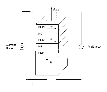
Figure 4 is an illustration of a memory cell according to one embodiment of
the present
invention;
Figures 5A-5E are illustrations of the free magnetic layer showing the
magnetization
vector and the demagnetizing field of the memory cell of Figure 4;
Figure 6A is an illustration of a current waveform that may be applied to the
memory cell
of Figure 4 during a write operation;
Figure 6B is an illustration of a resistance measured from the memory cell
during a read-
out operation before and after the current pulse shown in Figure 6A is
applied;
Figure 7 is an illustration of the free magnetic layer of a 4-state memory
cell;
Figure 8 is an illustration of an example of a current waveform applied to the
magnetic
device;
Figure 9 is an illustration of the magnetization components of the free
magnetic layer
during and after the application of the current pulse shown in Figure 8;
-6-
CA 02703696 2010-04-23
WO 2009/059071 PCT/US2008/081893
Figure 10 is an illustration of a memory cell according to one embodiment of
the present
invention in which during writing operations no net current passes through the
free magnetic layer;
Figure 11 is an illustration of an annular magnetic device according to the
present
invention;
Figure 12 is an illustration of an annular memory cell according to one
embodiment of the
present invention, and
Figure 13 is an illustration of an annular memory cell according to a further
embodiment
of the present invention in which separate read and write contacts are
provided.
DETAILED DESCRIPTION OF THE EMBODIMENTS
Structure of a Basic Magnetic Device
To illustrate the basic concept, Figure 1 shows a multilayered, pillar-shaped
magnetic
device comprising a pinned magnetic layer FM 1 with a fixed magnetization
direction and a free
magnetic layer FM2 with a free magnetization direction. in, Is the
magnetization vector of the
pinned magnetic layer FM 1, and m2 is the magnetization vector of the free
magnetic layer FM2.
The pinned magnetic layer FM 1 acts as a source of spin angular momentum.
The pinned magnetic layer FM1 and the free magnetic layer FM2 are separated by
a first
non-magnetic layer NI that spatially separates the two layers FM I and FM2
such that their mutual
magnetic interaction is minimized. The pillar-shaped magnetic device is
typically sized in
nanometers, e.g., it may be less than approximately 200 nm laterally.
The free magnetic layer FM2 is essentially a magnetic thin film element
imbedded in a
pillar-shaped magnetic device with two additional layers - the pinned magnetic
layer FM 1 and the
non-magnetic layer N l. The layer thicknesses are typically approximately 1 nm
to 50 nm.
These pillar-shaped magnetic devices can be fabricated in a stacked sequence
of layers by
many different means, including sputtering, thermal and electron-beam
evaporation through a sub-
micron stencil mask. These magnetic devices can also be fabricated in a stack
sequence using
sputtering, thermal and electron-beam evaporation to form a multilayered film
followed by a
-7-
CA 02703696 2010-04-23
WO 2009/059071 PCT/US2008/081893
subtractive nanofabrication process that removes materials to leave the pillar-
shaped magnetic
device on a substrate surface, such as that of a silicon of other
semiconducting or insulating wafer.
Materials for the ferromagnetic layers include (but are not limited to) Fe,
Co, Ni, and
alloys of these elements, such as Ni,_xFeX; alloys of these ferromagnetic
metals with non-magnetic
metals, such as Cu, Pd, Pt, NiMnSb, at compositions in which the materials are
ferromagnetically
ordered at room temperature; conducting materials; and conducting magnetic
oxides such as Cr02
and Fe304. For the nonmagnetic layers, materials include (but are not limited
to) Cu, Cr, Au, Ag,
and Al. The main requirement for the non-magnetic layer is the absence of
scattering of the
electron spin-direction on a short length scale, which is less than about the
layer thickness.
An electric current source is connected to the pinned magnetic layer FM 1 and
the free
magnetic layer FM2 so that an electric current I can traverse the pillar
device.
Method of Magnetic Switching
An electric current I is applied to the pillar-shaped magnetic device so that
the current I
flows through the various layers of the device, from the pinned magnetic layer
FM 1 to the first
non-magnetic layer N1 to the free magnetic layer FM2. The applied current I
results in a transfer
of angular momentum from the pinned magnetic layer FM 1 to the free magnetic
layer FM2. As
stated above, a transfer of angular momentum from one magnetic region to
another can produce a
torque.
Figures 2A-2E show steps in the method of magnetic switching using the
magnetic device
shown in Figure 1 and for convenience, Figures 2A-2E only show the free
magnetic layer FM2
and the magnetization vector m2 of the free magnetic layer FM2. Figure 2A
shows the initial
state of the free magnetic layer FM2 before the current I is applied.
As shown in Figures 2B-2D, applying a current I, which can be of a form as
shown in
Figures 3A and 3B, results in the transfer of angular momentum from the pinned
magnetic layer
FM 1 to the free magnetic layer FM2. This transfer of angular momentum from
the pinned
-8-
CA 02703696 2010-04-23
WO 2009/059071 PCT/US2008/081893
magnetic layer FM 1 to the free magnetic layer FM2 produces a torque zs on the
magnetic
moment of the free magnetic layer FM2.
The torque Fs per unit magnetization of the free layer is proportional to the
vector triple
product alm2 x (zn2 x tk) , where m2 is a unit vector in the direction of the
magnetic moment of
the free magnetic layer FM2 and rk is a unit vector in the direction of the
magnetic moment of
the pinned magnetic layer FM 1. The prefactor, a, , depends on the current I,
the spin-polarization
P of the current I, and the cosine of the angle between the free and pinned
magnetic layers, cos(h),
such that aI = hIg(P,cos(B))/(eMV). h is the reduced Planck's constant, g is a
function of the
spin-polarization P and cos(h), M is the magnetization density of the free
layer, e is the charge of
the electron, and V is the volume of the free layer (see, J. Slonczewski,
Journal of Magnetism and
Magnetic Materials 159, L1 (1996)). Thus, a large torque is is produced when
the magnetic
moments of the pinned magnetic layer FM 1 and the free magnetic layer FM2 are
perpendicular.
This torque Fs, which acts on the magnetic moment of the free magnetic layer
FM2,
causes the magnetization of the free magnetic layer FM2 to rotate out of the
plane of the layer.
Since the thickness of the free magnetic layer FM2 is less than the width and
length dimensions of
the free magnetic layer FM2, the rotation of the magnetization vector m2 of
the free magnetic
layer FM2 out of the plane of the layer generates a large magnetic field, a
'demagnetizing' field,
which is perpendicular to the plane of the layer.
This demagnetizing field forces the magnetization vector in-2 of the free
magnetic layer
FM2 to precess, i.e., to move such that the magnetization direction rotates
about the magnetic field
axis. The demagnetizing field also determines the rate of precession. A large
demagnetizing field
results in an extremely high precession rate, which is an optimal condition
for fast magnetic
switching.
Thus, in an optimal configuration of the magnetic memory device for fast
magnetic
switching, the magnetic moment of the pinned magnetic layer FM 1 is
perpendicular to the plane of
-9-
CA 02703696 2010-04-23
WO 2009/059071 PCT/US2008/081893
the free magnetic layer FM2, and the magnetic moment of the free magnetic
layer FM2 is
perpendicular to the axis of the pillar of thin layers and lies in the plane
of the free magnetic layer
FM2.
Figure 2E shows the free magnetic layer FM2 after the magnetic switching
process is
completed. As shown in Figures 2A and 2E, the magnetic switching process
causes the
magnetization vector m2 of the free magnetic layer FM2 to switch by reversing
direction by
rotating 180'.
Figures 3A and 3B show two different forms of current input that may be
applied to the
magnetic device. The current input shown in Figure 3A is comprised of two
current pulses of
short duration, a first positive current pulse followed by a second negative
current pulse. This
form of current input results in writing a '1' or a `0'. Alternatively, the
first current pulse can be
negative and the second current pulse can be positive, as long as the two
current pulses are of
opposite polarity. In both cases, the state of the magnetic bit will be
changed from `1' to `0' or `0'
to `1' (i.e., the final state will be the complement of the initial state of
the bit). The current input
shown in Figure 3A is used in the method of magnetic switching described above
and shown in
Figures 2A-2E. Using a current input formed of two current pulses results in a
faster magnetic
switching process.
The first current pulse starts the precession of the magnetization vector m2
of the free
magnetic layer FM2. After the completion of the first current pulse, the
second current pulse is
applied to stop the precession at a desired state.
The second current pulse is not essential to the operation of the device, but
it enables
higher speed switching. For example, the current input shown in Figure 3B is
comprised of a
single positive current pulse. Alternatively, a single negative current pulse
may also be applied to
the magnetic device. Simulations show that many different types of current
pulses switch FM2.
Therefore device operation is certainly not limited to the current pulses
shown in Figure 3.
-10-
CA 02703696 2010-04-23
WO 2009/059071 PCT/US2008/081893
Structure of a Memory Cell
The magnetic device described above can be incorporated into a memory cell for
inclusion
into arrays of memory cells to make up a magnetic memory. According to one
embodiment as
shown in Figure 4, the magnetic device of the present invention, when
implemented as a memory
cell, is a multilayered, pillar-shaped device having a pinned magnetic layer
FM 1 with a fixed
magnetization direction, a free magnetic layer FM2 with a free magnetization
direction, and a
read-out magnetic layer FM3 with a fixed magnetization direction. m is the
magnetization vector
of the pinned magnetic layer FM1, m2 is the magnetization vector of the free
magnetic layer
FM2, and m3 is the magnetization vector of the read-out magnetic layer FM3.
The pinned magnetic layer FM 1 and the free magnetic layer FM2 are separated
by a, first
non-magnetic layer N1 that spatially separates the two layers FM1 and FM2 such
that their mutual
magnetic interaction is minimized. The free magnetic layer FM2 and the read-
out magnetic layer
FM3 are separated by a second non-magnetic layer N2 that spatially separates
the two layers FM2
and FM3 such that their mutual magnetic interaction is minimized. The pillar-
shaped magnetic
device is typically sized in nanometers, e.g., it may be less than
approximately 200 nm.
An electric current source is connected to the pinned magnetic layer FM 1 and
the read-out
magnetic layer FM3 so that an electric current I can traverse the pillar
device. A voltmeter is
connected to the pinned magnetic layer FM1 and the read-out magnetic layer FM3
so that the
resistance of the magnetic device can be measured to thereby read the logical
contents of the
memory cell.
Method For Writing Information
The magnetic switching process is used when information is written into a
memory cell.
To store a logical bit of information in a memory cell, the magnetization
direction of the
magnetization vector inside the memory cell is set in one of two possible
orientations to code the
logical values of '0' and ' 1' . This magnetic device, when implemented as a
memory cell, uses the
method of magnetic switching described previously in order to store bits of
information. Current
- 11 -
CA 02703696 2010-04-23
WO 2009/059071 PCT/US2008/081893
pulses are applied to change the logical value in the magnetic device. The
magnetic memory
device described above and shown in Figure 4 stores one bit of information
since the free magnetic
layer FM2 has a single magnetization vector m2 with two stable magnetic
states.
An electric current I is applied to the pillar-shaped magnetic memory device
so that the
current I flows through the various layers of the magnetic memory device, from
the pinned
magnetic layer FM1 to the read-out magnetic layer FM3. The applied current I
results in a
transfer of angular momentum from the pinned magnetic layer FM 1 to the free
magnetic layer
FM2.
Figures 5A-5E show steps in the method of writing information using the
magnetic
memory device shown in Figure 4 and for convenience, Figures 5A-5E only show
the free
magnetic layer FM2 and the magnetization vector in-2 of the free magnetic
layer FM2. Figure 5A
shows the initial state of the free magnetic layer FM2 before the current I is
applied.
As shown in Figures 5B-5D, applying a current I, which can be of a form as
shown in
Figures 3A and 3B, results in the transfer of angular momentum from the pinned
magnetic layer
FM I to the free magnetic layer FM2. Figures 2A-2E and 5A-5E show the change
in the
orientation of the magnetization vector m2 of the free magnetic layer FM2 as a
result of applying
the current to the magnetic device.
Figure 6A shows a form of the current input that is applied to the magnetic
memory device
shown in Figure 4. The current input of Figure 6A includes two current pulses
of short duration,
a first positive current pulse followed by a second negative current pulse,
which results in writing
a '1' or a `0'. Alternatively, the first current pulse can be negative and the
second current pulse
can be positive, as long as the two current pulses are of opposite polarity.
In both cases, the state
of the magnetic bit will be changed from `1' to `0' or `0' to `1' (i.e., the
final state will be the
complement of the initial state of the bit).
The first current pulse starts the precession of the magnetization vector in2
of the free
magnetic layer FM2. After the completion of the first current pulse, the
second current pulse is
applied to stop the precession at a desired state. For this embodiment of the
magnetic memory
-12-
CA 02703696 2010-04-23
WO 2009/059071 PCT/US2008/081893
device of the present invention, the precession is stopped when 180 rotation
of the magnetization
vector m2 of the free magnetic layer FM2 is achieved.
Figure 6B shows an example of the corresponding resistance of the device as
measured by
the voltmeter connected to the magnetic memory device shown in Figure 4 with a
small current
applied, i.e., a current intensity much less than that used in the current
pulses. The resistance
increases after the current pulses of Figure 6A are applied to the device. At
the initial state shown
in Figure 5A (before the first positive current pulse), the resistance is at a
constant low value. At
the final state shown in Figure 5E, the resistance is at a constant high
value.
Thus, the states shown in Figures 5A and 5E correspond to a logical value of
"0" in the
initial state and a logical value of " 1 " in the final state, respectively.
The magnetization vector m2
of the free magnetic layer FM2 in the final state shown in Figure 5E is in the
opposite direction
than the magnetization vector m2 of the free magnetic layer FM2 in the initial
state shown in
Figure 5A.
The necessary amplitude of the current pulses can be estimated by numerical
modeling
using the equations of micromagnetics, the Landau-Lifzshitz Gilbert equations
including the spin-
transfer torque discussed earlier (see, for example, B. Oezyilmaz et al.,
Phys. Rev. Lett. 91,
067203 (2003)). For a free layer comprised of Co with a magnetization density
of M = 1400
emu/cm3, a Gilbert damping parameter a of 0.01, a spin-polarization of the
current P of 0.4, and
an in-plane uniaxial anisotropy field of 1000 kOe. (In this case, the in-plane
uniaxial anisotropy
constant K is K=7 x 10⁵ erg/cm3.) For the purposes of this estimation, the Co
free layer is 3 nm
thick and has lateral dimensions of 60 rim by 60 nm. We find that a current
pulse of amplitude of
5 mA is more than sufficient to switch the layer. The current necessary to
switch the device is
reduced by decreasing the size of the Co free layer; increasing the spin-
polarization of the current,
for example, by using a pinned layer with a higher degree of spin-
polarization; and decreasing the
in-plane anisotropy or decreasing the Gilbert damping. For this current
amplitude, a 35 psec pulse
is sufficient to switch the device.
-13-
CA 02703696 2010-04-23
WO 2009/059071 PCT/US2008/081893
With a device resistance of 5 Ohms, the energy dissipation is 5 x 10-15 J.
This energy
dissipation value can be compared to the energy needed to switch a magnetic
device with a spin-
polarized current when the pinned layer and the free layer magnetizations are
initially aligned
along the same axis. Recent experiments show that this requires a current of
approximately 10
mA applied for approximately 10 ns in a device with a resistance of 5 Ohms
(see, R. H. Koch et
al. Phys. Rev. Lett. 92, 088302 (2004)). The energy dissipated is thus 5 x 10-
12 J. Thus, in
comparison, the power requirement for our device is quite small. Further,
because the pulse is on
only very briefly, in spite of the large current densities, 1 A/ m2, no
electromigration is expected.
Further, we have operated such devices at current densities 5 times greater
than this value for
extended periods (approximately 1 minute) with no device damage (see, B.
Oezyilmaz et al., Phys.
Rev. Lett. 91, 067203 (2003)).
Method For Reading Information
The read-out magnetic layer FM3 is required in the simplest implementation of
the
magnetic memory device. The read-out magnetic layer FM3 has a magnetization
vector m3 with a
fixed magnetization direction. The magnetization vector m3 of the read-out
magnetic layer FM3
can be fixed in a number of ways. For example, the read-out magnetic layer FM3
can be formed
thicker or of a higher anisotropic magnetic material or can be placed adjacent
to an
antiferromagnetic layer to use the phenomena of exchange biasing. In the
phenomena of exchange
biasing, the coupling between the antiferromagnetic layer and the
ferromagnetic layer and the large
magnetic anisotropy of the antiferromagnetic layer results in a hardening of
the ferromagnetic
layer so that larger magnetic fields and currents are required to change its
magnetization direction.
The resistance of the magnetic memory device is very sensitive to the relative
orientation
of the magnetization vector m2 of the free magnetic layer FM2 and the
magnetization vector m3
of read-out magnetic layer FM3. The resistance of the magnetic memory device
is highest when
the magnetization vectors m2 and r'rc3 of the free magnetic layer FM2 and the
read-out layer FM3,
-14-
CA 02703696 2010-04-23
WO 2009/059071 PCT/US2008/081893
respectively, are in anti-parallel alignment. The resistance of the magnetic
device is lowest when
the magnetization vectors n22 and in-3 of the layers FM2 and FM3,
respectively, are in parallel
alignment. Thus, a simple resistance measurement can determine the orientation
of the
magnetization vector in-2 of the free magnetic layer FM2.
The fixed orientation of the magnetization vector m3 of the read-out magnetic
layer FM3
is set so that it is either in parallel or anti-parallel alignment with the
magnetization vector m2 of
the free magnetic layer FM2, depending on the orientation of the magnetization
vector m2 of the
free magnetic layer FM2. Since the orientation of the magnetization vector m2
of the free
magnetic layer FM2 switches so that it can be rotated 180 , the magnetization
vectors rn2 and m3
of the free magnetic layer FM2 and the read-out layer FM3, respectively, must
be in either anti-
parallel or parallel alignment.
Storage of Multiple Bits of Information
The magnetic memory device described above and shown in Figure 4 has two
stable
magnetic states and is able to store one bit of information. According to
another embodiment of
the present invention, a magnetic memory device can be constructed to store
multiple bits of
information. FIG. 7[[6]] shows an example of a free magnetic layer FM2 with
four stable
magnetic states. A magnetic memory device comprising a free magnetic layer FM2
with four
stable magnetic states is able to store two bits of information. In this
embodiment, current pulses
are applied to switch the magnetization between directions that differ by 90
instead of 180 .
This can be accomplished by current pulses of a different form. For example,
the current pulses
can be smaller in amplitude and/or shorter in duration. The readout layer
(FM3) is then aligned
such that each of the four magnetization states has a different resistance.
This requires that the
-15-
CA 02703696 2010-04-23
WO 2009/059071 PCT/US2008/081893
readout layer magnetization not have an in-plane component that points
parallel to any of the
four states nor at 45 to these states.
Example
The operation of the magnetic device was simulated using Landau-Lifzshitz
Gilbert
equations including a spin-transfer torque.
Figure 8 shows the amplitude of the current input applied to the magnetic
memory device
starting at an initial time t=0 and ending at t=30 picoseconds. This current
input comprises two
current pulses similar to the current input shown in Figures 3A and 6A.
A 16-picosecond positive current pulse is applied to the magnetic memory
device to start
the precession of the magnetization vector in-2 of the free magnetic layer
FM2. After this 16-
picosecond current pulse, a 14-picosecond negative current pulse is applied to
the magnetic
memory device to stop the precession of the magnetization vector in-2 of the
free magnetic layer
FM2 to achieve a desired state of the magnetization vector m2 . For magnetic
memory devices,
the precession is stopped after achieving a 180 rotation of the magnetization
vector in-2 of the
free magnetic layer FM2.
Figure 9 shows the magnetization components mx and my of the magnetization
vector
in-2 of the free magnetic layer FM2 in the x- and y-directions shown in
Figures 2B and 5B. The
magnetization components mX and my are measured during and after the
application of the
current input shown in Figure 8. Figure 9 shows that the magnetization vector
m2 of the free
magnetic layer FM2 reverses 180 from the initial state, which corresponds to
Figure 5A, to the
final state, which corresponds to Figure 5E. The magnetization components (mx
, my) are able to
switch between (-1,0) to (1,0) as shown by the present invention.
-16-
CA 02703696 2010-04-23
WO 2009/059071 PCT/US2008/081893
Advantages
The high speed, low power magnetic device of the present invention uses energy
only for
read and write operations or logic operations. When not energized, the
information is stored
without significant loss. Thus, the magnetic device of the present invention,
when implemented as
a memory cell, can be used as a non-volatile memory.
The non-volatile memory provided by the magnetic device of the present
invention is
suitable for many applications, such as in computers and portable electronic
devices. In particular,
the high speed, low power magnetic device of the present invention provides
several advantages.
The performance of the high speed, low power magnetic device of the present
invention compares
favorably with flash memory and other types of non-volatile random access
memory (RAM), such
as conventional magnetic RAM (MRAM) and ferroelectric RAM (FRAM).
The current-induced torques act only on the magnetic device that is energized,
i.e., to
which a current is applied. Therefore, when multiple magnetic devices are
arranged in an array,
such as in magnetic memory, the current-induced spin transfer does not produce
parasitic
interactions ("cross-talk") between the neighboring elements in the array,
unlike in conventional
magnetic memories in which magnetic switching is accomplished by using
magnetic fields
produced by small current-carrying wires near the magnetic elements.
The method of magnetic switching by current induced torque provided by the
present
invention is faster than current conventional methods that use magnetic fields
to switch the
magnetization direction of layers. Read-out and write operations of the
present invention can be
completed in sub-nanosecond time scales. Conventional magnetic hard drives are
very slow
compared to the magnetic memory of the present invention since the
conventional hard drives have
data access times of the order of milliseconds.
The method of magnetic switching by current induced torque provided by the
present
invention requires low power. This is especially advantageous for use in
portable electronic
devices.
The method of magnetic switching by current induced torque provided by the
present
invention is ideal for sub-micron scale devices since the lateral dimension of
the magnetic device
-17-
CA 02703696 2010-04-23
WO 2009/059071 PCT/US2008/081893
of the present invention may be less than approximately 200 nm. Therefore, the
present invention
is scaled to allow the fabrication of ultra-high density memory cells so that
a vast amount of
information can be stored in the magnetic memory provided by the present
invention.
The basic architecture of the high speed, low power magnetic device of the
present
invention is straightforward, and read-out and write operations are reliable
and are less sensitive to
changes in temperature. Unlike conventional magnetic memory devices, the
present invention
does not rely on stochastic (random) processes or fluctuating fields to
initiate switching events.
According to one embodiment of the present invention, multiple bits of
information can be
stored on each device so that even more information can be stored in the
magnetic memory.
The method of magnetic switching by current induced torque provided by the
present
invention can be used for logic operations, as well as for magnetic memory
devices. Since there is
a threshold, which is dependent on the shape, amplitude, and period of the
current pulse, for the
current pulse to produce a change in magnetization, current input can be
combined to produce a
logic function, such as an AND gate. For example, two current pulses can be
combined to
produce a current pulse that traverses the device which is the sum of the two
current pulses. The
pulse characteristics (shape, amplitude, and period) can be chosen such that
each pulse individually
does not switch the device, yet the combined pulse does switch the device.
Thus, this is an AND
operation. A NOT operation requires simply switching the state of the device..
A NOT and an
AND operation can be combined to produce a NAND function, which is a universal
digital logic
gate (i.e., all digital logic functions can be constructed from NAND gates.)
There are several possible geometries and layer configurations that are
provided by the
present invention. For example, an embodiment of the magnetic device of the
present invention
may be configured so that no net current passes through the free magnetic
layer FM2 during write
operations. This is illustrated in Fig. 10 which shows an embodiment of the
present invention
including current source A, current source B, and layer 12, which is a thin
insulating layer made of
A1203, for example. In this device, layer 12 is 0.5 to 3 nm thick and is thin
enough so that
electrons can traverse the layer by quantum mechanical tunneling.
-18-
CA 02703696 2010-04-23
WO 2009/059071 PCT/US2008/081893
In the device shown in Fig. 10, current pulses are applied with current source
A to change
the magnetization direction of the free magnetic layer FM2. Using current
source A, current
flows from FM I to the non-magnetic layer N1 and electron spin angular
momentum is transferred
to the free magnetic layer FM2 by reflection of electrons at the interface
between the non-magnetic
layer N1 and the free magnetic layer FM2. The device readout is performed
using current source
B. The voltage is measured when a small current from B passes between the free
magnetic layer
FM2 and the readout layer FM3. This voltage will depend on the relative
magnetization directions
of the layers FM2 and FM3 so that the magnetization direction of the free
magnetic layer FM2 can
be determined to read-out the device. This device has the advantage that the
readout signal is large
since the tunnel junction resistance can be large (1 Ohm to 100 kOhm). Readout
signals can be in
the range from 10 mV to 1 V.
Structure of an Annular Magnetic Device
A pillar-shaped magnetic device 1100 having a closed periodic structure is
illustrated in
Figure 11. Magnetic device 1100 includes a free magnetic layer 1110, a non-
magnetic layer
1120, and a reference magnetic layer 1130. The reference layer 1130 preferably
has a fixed
magnetic helicity 1135, a magnetic vector with a fixed direction at a
predetermined angle, for
example, perpendicular to the plane of the layer, or both a fixed magnetic
helicity 1135 and a
magnetic vector having a fixed direction at a predetermined angle. The free
magnetic layer
1110 preferably has a free magnetization helicity 1115. The reference layer
1130 preferably
acts as a source of spin angular momentum. The free layer 1110 and the
reference layer 1130
are preferably separated by non-magnetic layer 1120.
The reference layer 1130 is preferably magnetically harder than the free layer
1110 and
preferably has a well-defined magnetic state. This property can be achieved,
for example, by
using a layer that is thicker than the free layer or a material having a
larger magnetic
anisotropy than the material of the free layer 1110, such as Cobalt, the L10
phase of FePt or
-19-
CA 02703696 2010-04-23
WO 2009/059071 PCT/US2008/081893
FePd, or layered structures of Cobalt and Nickel. Alternatively, the desired
hardness can be
achieved through exchange coupling to a thin anti-ferromagnetic layer, such as
IrMn or FeMn.
The non-magnetic layer 1120 preferably conserves spin-momentum of the
reference
magnetic layer 1130 during spin transport across the non-magnetic layer 1120.
Thus, the spin
diffusion length of the material used in the non-magnetic layer 1120 is
preferably longer than
the thickness of the non-magnetic layer 1120. Examples of materials that
satisfy the desired
properties include any of the noble metals (e.g., Cu, Ag, Au). The non-
magnetic layer may
also be an insulator such as A1203 or MgO. For a sufficiently thin insulating
layer the spin
transport will occur by electron tunneling so as to form a magnetic tunnel
junction.
The free magnetic layer 1110 preferably includes a soft magnetic material
having a
large exchange length, such as permalloy, cobalt, nickel, iron, and alloys of
those materials.
Additionally, alloys including non-magnetic elements, such as copper, may
advantageously
reduce the magnetic moment of the layers. Alternatively the free magnetic
layer can include
magnetic oxides such as Cr02 or Fe304.
As illustrated in Figure 11, each layer of the magnetic device 1100 is
preferably ring-
shaped (i.e. annular). An annular shape can minimize the number of edges or
sharp corners
that may act as magnetic nucleation sites which reduces stability by
increasing the rate of
reversal of magnetic helicity. A symmetrical ring structure is one of the
preferred shapes
which can be used to avoid unwanted reversal of helicity, however the present
invention may
employ many various forms of closed period structures which may provide
similar advantages.
The lower the rotational symmetry of the shape of the device, the more likely
it is that certain
regions will be favored for magnetic nucleation and reversal of magnetic
helicity. Geometries
that include sharp corners provide strong nucleation sites that encourage
helicity reversal and
are preferably avoided.
Typically devices that are known in the art result in a tradeoff between the
stability of
the stored information represented by the free magnetic layer helicity 1115
and the speed and
-20-
CA 02703696 2010-04-23
WO 2009/059071 PCT/US2008/081893
power requirements of changing the information. Typically, as the stability of
the
programmed helicity increases, so does the power required to change the
helicity.
Ring geometries may provide very stable magnetization orientations.
Additionally, the
magnetization reversal mechanism of ring geometries may be weakly dependent on
ring
diameter beyond a critically small size (e.g., typically tens of nanometers).
Thus, the size of
the device may not be a critical a factor when compared with most presently
used geometries.
Thus, ring geometries may enable a greater range of use and decreased
production costs.
Several factors play a role in the stability of the magnetization of a ring.
One factor
may be the size of the ring. For a given magnetic field, there exists a
critical ring radius for
which a ring having a radius equal to or greater than the critical size, the
stability of the
magnetization of the ring is relatively independent of the ring size. The
stability of the
magnetization may decrease rapidly as the size of the ring decreases below the
critical size.
Additionally, the magnetization may be susceptible to thermal fluctuations and
the application
of a destabilizing magnetic field.
Utilizing these properties, a ring-shaped magnetic device can be designed for
which the
magnetization of the device is generally stable under static operating
conditions, but can easily
be changed or reversed by applying a current pulse to the device.
Specifically, for a ring
device that is substantially near the critical size with no applied current,
the magnetic helicity
can be easily reversed by applying an electrical current. The electrical
current has the effect
of providing a destabilizing field and effectively changing the value of the
critical radius of the
ring. Thus, a magnetic ring designed near the critical size is stable and does
not experience
unwanted reversal under normal operating conditions, but can be reversed by
the application
of a relatively small current.
In another aspect of this invention, a magnetic ring device that has a radius
greater than
or equal to the critical radius can provide a very stable magnetization. Thus,
if it is not a goal
of the device to modify or reverse the magnetization of the device, a magnetic
ring having a
-21-
CA 02703696 2010-04-23
WO 2009/059071 PCT/US2008/081893
radius that is greater than the critical radius, can be easily employed in
read only memory in a
wide range of sizes greater than the critical size.
Figure 12 illustrates a magnetic ring device 1200 employed as a magnetic
memory
element. Preferably, the free magnetic layer 1210 has a magnetic helicity 1215
with at least
two stable orientations - a clockwise orientation and a counter-clockwise
orientation. The
reference layer 1230 preferably has a magnetic vector having a fixed direction
at
predetermined angle 1236, a fixed magnetic helicity 1235, or both a fixed
magnetic vector
having a direction at a predetermined angle 1236 and a fixed magnetic helicity
1235.
Preferably, the predetermined angle of the fixed magnetic vector 1236 is
substantially
perpendicular to the plane of the reference layer 1230. The reference magnetic
layer 1230 and
the free magnetic layer 1210 are preferably separated by a non-magnetic layer
1220.
The direction of the free magnetic layer helicity can be changed or reversed
by
applying an electrical pulse across the layers of magnetic device 1200 from
current source
1270. The pulse from control current source 1270 may initiate the reversal of
the free
magnetic layer helicity 1215. The spin-momentum of the reference magnetic
layer 1230 may
be transferred to the free magnetic layer 1210 so as to change the
magnetization and induce
reversal of the free magnetic layer helicity 1215. An electrical pulse in one
direction across
the device 1200 may set the free magnetic layer helicity 1215 in a clockwise
direction, and an
electrical pulse in the opposite direction may set the free magnetic layer
helicity 1215 in a
counter-clockwise direction.
The electrical pulse from control current source 1270 may initiate the
reversal of the
free magnetic layer helicity 1215. Reversal of the free magnetic layer
helicity 1215 may stop
when the second stable state is reached. However, a second current pulse from
control current
source 1270 can be used to stop the reversal of the free magnetic layer
helicity 1215 more
quickly. A reference layer 1230 having an easy axis 1236 (i.e., the
energetically favorable
direction of the spontaneous magnetization in a ferromagnetic material) that
is substantially
-22-
CA 02703696 2010-04-23
WO 2009/059071 PCT/US2008/081893
perpendicular to the free magnetic layer 1210 can lead to faster spin-transfer
induced reversal
of the free magnetic layer helicity 1215.
A second reference layer 1263 with fixed magnetic layer helicity 1268 may be
used to
read-out the helicity state of the free magnetic layer. The fixed magnetic
helicity can be
achieved, for example, by using a layer that is thicker than the free layer or
a material having
a larger magnetic anisotropy than the material of the free layer 1210, such as
Cobalt, the L10
phase of FePt or FePd, or layered structures of Cobalt and Nickel. The second
reference 1263
layer is preferably separated from the free magnetic layer 1210 by a non-
magnetic layer 1266,
which may be a thin non-magnetic metal or insulating layer. In the case of an
insulating layer,
the second reference layer 1263 and the free magnetic layer 1210 form a
magnetic tunnel
junction. If the free magnetic layer helicity 1215 and the second reference
magnetic layer
helicity 1268 are in the same direction (i.e., the magnetic helicities are
both clockwise or both
counter-clockwise), the resistance across the device 1200 may be generally
smaller than if the
free magnetic layer helicity 1215 and the reference magnetic layer helicity
1235 are in
opposite directions, thereby differentiating between the two stable
orientations of the free
magnetic layer 1210.
Figure 13 illustrates a further embodiment of a magnetic ring device 1300
employed as
a magnetic memory element in accordance with the present invention.
Preferably, the free
magnetic layer 1310 has at least two stable orientations of the free magnetic
layer helicity 1315
- a clockwise orientation and a counter-clockwise orientation. The reference
layer 1330
preferably has a fixed magnetic vector 1336 having a direction at a
predetermined angle, a
fixed magnetic helicity 1335, or both a fixed magnetic vector 1336 having a
direction at a
predetermined angle 1336 and a fixed magnetic helicity 1335. Preferably, the
predetermined
angle of the fixed magnetic vector 1336 is substantially perpendicular to the
plane of the
reference layer 1330. The reference magnetic layer 1330 and the free magnetic
layer 1310 are
preferably separated by a non-magnetic layer 1320.
-23-
CA 02703696 2010-04-23
WO 2009/059071 PCT/US2008/081893
The direction of the free magnetic layer helicity can be changed or reversed
by
applying an electrical pulse across the layers of magnetic device 1300 from
control current
source 1370 through write contact 1350 and contact 1340. The pulse from
control current
source 1370 may initiate the reversal of the free magnetic layer helicity
1315. The spin-
momentum of the reference magnetic layer 1330 may be transferred to the free
magnetic layer
1310 so as to change the magnetization and induce reversal of the free
magnetic layer helicity
1315. An electrical pulse in one direction across the device 1300 may set the
free magnetic
layer helicity 1315 in a clockwise direction, and an electrical pulse in the
opposite direction
may set the free magnetic layer helicity 1315 in a counter-clockwise
direction.
The electrical pulse from control current source 1370 may initiate the
reversal of the
free magnetic layer helicity 1315. Reversal of the free magnetic layer
helicity 1315 may stop
when the second stable state is reached. However, a second current pulse from
control current
source 1370 can be used to stop the reversal of the free magnetic layer
helicity 1315 more
quickly.
A reference layer 1330 having an easy axis (i.e., the energetically favorable
direction
of the spontaneous magnetization in a ferromagnetic material) that is
substantially
perpendicular to the free magnetic layer 1310 can lead to faster spin-transfer
induced reversal
of the free magnetic layer helicity 1315.
Current injection need not be symmetric. Local injection of the current may be
used to
initiate the change in the free magnetic layer helicity 1315. Transfer of spin
angular
momentum may serve to nucleate magnetization reversal with current spin-
polarized by the
reference layer 1330. Layer 1320 is a spin preserving non-magnetic layer such
as Cu, Ag, Au
or a thin insulating layer such as A1203 or MgO. Small asymmetry in the ring
may facilitate
nucleation and reversal through spin-momentum transfer. Pronounced asymmetry
could reduce
the magnetization stability, which is undesirable.
The state of the free magnetic layer helicity can be determined by measuring
the
voltage or resistance across the device 1300. If the free magnetic layer
helicity 1315 and the
-24-
CA 02703696 2010-04-23
WO 2009/059071 PCT/US2008/081893
reference magnetic layer helicity 1335 are in the same direction (i.e., the
magnetic helicities
are both clockwise or both counter-clockwise), the resistance across the
device 1300 may be
generally smaller than if the free magnetic layer helicity 1315 and the
reference magnetic layer
helicity 1335 are in opposite directions.
Currently available magnetic memory devices typically require relatively high
currents
and low impedance to write information (i.e., modify the magnetic helicity of
the device),
whereas readout is done with smaller currents but requires a large readout
signal. The ring
geometry of the magnetic device 1300 addresses these contradicting
requirements by allowing
the performance of the reading and writing operations in different locations
on the device. A
write operation can be performed by control current source 1370, which
provides a large
current, and write contact 1350, which can be in direct contact with either
the free magnetic
layer 1310 or the reference magnetic layer 1330 thus having low impedance. The
write
operation circuit is completed through contact 1340 which can be placed in
direct contact with
either the free magnetic layer 1310 or the reference magnetic layer 1330 to
complete the
circuit across device 1300.
The read operation can be performed using a separate readout circuit. Read
contact
1360 can include a magnetic contact portion 1363 with a fixed magnetization
direction or
helicity 1365 and an insulator portion 1366 that separates the magnetic
contact 1363 from the
device 1300, thereby forming a magnetic tunnel junction with the device 1300.
A separate
readout current source 1380 can provide a smaller current across the device
1300 which is
measured by voltage or resistance readout 1390.
Preferably, the thickness of the device is approximately 10 to 200 nanometers
and has
an outer radius of approximately 0.25 to 1 micron.
Typical multi-element magnetic devices have strong magnetostatic interaction
between
the different elements. This interaction can be difficult to quantify or
control, and thus results
in problems increasing density and performance of the device. The present
invention may
minimize these interactions. Additionally, the device avoids the problems of
magnetic field
-25-
CA 02703696 2010-04-23
WO 2009/059071 PCT/US2008/081893
spreading which results in superior speed writing and readout along with
reduction of error
due to stray or poorly controlled fields.
While there has been described what are at present considered to be
embodiments of the
present invention, it will be understood that various modifications may be
made thereto, and it is
intended that the appended claims cover all such modifications as fall within
the true spirit and
scope of the invention.
Magnetic tunnel junctions offer the possibility of very large
magnetoresistance that can
be used to read the state of a magnetic memory cell. A magnetic tunnel
junction consists of
two magnetic layers separated by a thin insulating layer. The insulator is
sufficiently thin that
electrons may traverse this layer by quantum mechanical tunneling. The
thickness of the
insulator is typically between 0.3 and 3 nm.
A large magnetoresistance will provide a large readout signal. It has been
shown
experimentally that very large magnetoresistance can be achieved using
magnesium oxide
(MgO) insulating barriers. The magnetoresistance refers to the percentage
change in resistance
between states in which the layers are magnetized antiparallel and parallel. A
magnetoresistance of greater that 400% has been achieved recently with MgO
insulating
layers. With an aluminum oxide insulating layer, a magnetoresistance of about
30% has been
achieved. Either of these materials as well as other insulators may prove
useful as the non-
magnetic layers, NI or N2..
Note that current must pass through the insulating layer during the switching
process.
An exception to this is the device represented in Fig. 10, in which there is a
separate electrical
contact to Ni. This means the insulator must not be damaged in the presence of
this current
or, equivalently, the voltage that appears across the junction in the presence
of the current.
Thin insulating barriers typically support 1V/mm electric fields before
damage, known as
voltage breakdown. The current required to switch the junction must not
produce electric
fields in the junction that exceed the insulator breakdown electric field.
The pinned magnetic layer of the device may include a material with a
perpendicular
magnetic anisotropy. A perpendicular magnetic anisotropy gives a preference
for the
magnetization to orient perpendicular to the plane of the layer. Thin magnetic
layers are
typically magnetized in the film plane. This orientation is usually a lower
energy
configuration; it reduces the layer's magnetostatic energy. To orient the
magnetization
perpendicular to the plane the perpendicular magnetic anisotropy must be
sufficiently large
compared to the magnetostatic energy of the layer.
-26-
CA 02703696 2010-04-23
WO 2009/059071 PCT/US2008/081893
This can be achieved with a number of different materials. For example, alloys
of Fe
and Pt, Fe and Pd, Co and Pt, Co and Pd, Co and Au, Co and Ni. This can also
be achieved
by creating interfaces between dissimilar magnetic materials or magnetic
materials and non-
magnetic materials. An example of the former, is layered structures of Co and
Ni and example
of the latter is layered structure of Co and Au or Co and Pt. An advantage of
these layered
materials is that they need not be crystalline; polycrystalline layers
suffice.
This layer serves to spin polarize the current. The materials should have good
spin
polarization efficiency. A disadvantage of using Pd or Pt is that these
elements typically induce
strong spin-scattering which reduces the layer spin-polarization. Large layer
spin-polarization
is needed for efficient device operation.
The free layer's magnetization direction switches in response to a current
pulse. It is
desirable to reduce the amplitude of this current pulse to lower the power
required for device
operation. Current requirements are linked to the magnetization density,
damping and
magnetic anisotropy of the layers. The lower the magnetization density and
magnetic
anisotropy the lower the required current amplitude for switching. The
magnetization density
of a magnetic is lowered if the magnetic material is alloyed with a non-
magnetic material. (Of
course, this only holds in a range of alloy concentrations. Eventually the
material will become
non-magnetic.)
It should be noted that the switching current amplitude and switching time are
interdependent. For example, lower magnetization density increases the time to
reverse the
magnetization.
It may be desirable to increase the magnetization damping of the free magnetic
layer to
increase the device reliability. It is the expectation that increasing the
damping would increase
the parameter range for switching. That is, the device would switches
reproducibly between
states for a greater range of current pulse amplitudes, times and current
pulse shapes.
The following references are hereby incorporated by reference in their
entirety: [1] S.
Yuasa et al, Appled Physics Letters 89, 042505 (2006); [2] J-M. L. Beaujour ,
W. Chen, K.
Krycka, C-C. Kao, J. Z. Sun and A. D. Kent, "Ferromagnetic resonance study of
sputtered
Co I Ni multilayers," The European Physical Journal B, DOI: 10.1140 (2007);
and [3] ] J-M.
L. Beaujour, A. D. Kent and J. Z. Sun, "Ferromagnetic resonance study of
polycrystalline
Fe_{1-x}V_x alloy thin films" arXiv:0710.2826 (October 2007)
-27-