Note: Descriptions are shown in the official language in which they were submitted.
CA 02703788 2010-04-26
DESCRIPTION
POWER SUPPLY CONTROLLER
Technical Field
This invention relates to a power supply controller, and more particularly, to
a power
supply controller for controlling power supply from a plurality of solar cell
arrays and a battery
to a load.
Background Art
As illustrated in FIG. 5, an associated power supply controller is connected
to a solar
cell 51, a battery 52, and a load 53, and includes (a plurality of) shunt
circuits 54, a driver circuit
55, a charging circuit 56, and a discharging circuit 57.
In the power supply controller, an output voltage (bus voltage) of the solar
cell 51 is
stabilized by the shunt circuit 54 to be supplied to the load 53, and supplied
to the charging
circuit 56 to charge the battery 52. In order to realize constant current and
constant voltage
control, the charging circuit 56 includes a switching regulator (battery
charge regulator (BCR)).
The operation of the shunt circuit 54 and the charging circuit 56 is
controlled by the
driver circuit 55 having a redundant circuit structure with high failure
resistance. When the
output power of the solar cell 51 exceeds load power and then a voltage of a
capacitor bank
(which is not shown and connected in parallel with load) increases, the driver
circuit 55 first
causes the charging circuit 56 to be turned ON to charge the battery 52 with
excess power.
When the excess power increases, the driver circuit 55 causes the shunt
circuit 54 to be tuned
ON to consume the excess power (by short circuit). When the output power of
the solar cell 51
is smaller than the load power, power is supplied from the battery 52 to the
load 53 through the
discharging circuit 57 (for example, discharge diode).
The power supply controller illustrated in FIG. 5 is of a type frequently used
for mainly
a low-earth orbit satellite having a large charging current (see Patent
Document 1).
There is another associated power supply controller as illustrated in FIG. 6.
The power
supply controller illustrated in FIG. 6 is connected to not only the solar
cell 51, the battery 52,
and the load 53 but also a solar cell (charge array) 61 for only charging and
includes a charging
circuit 62 having a simple switch instead of the charging circuit 56
illustrated in FIG. 5.
The battery 52 is charged by the solar cell 61 for only charging through the
charging
circuit 62. When the battery 52 is fully charged and the charging circuit 62
is turned OFF,
CA 02703788 2013-07-26
74927-22
2
power from the solar cell 61 may be supplied to the load 53.
The power supply controller illustrated in FIG. 6 is of a type frequently used
for mainly a geostationary orbit satellite having a small charging current
(see Patent
Document 1).
In any of the power supply controllers described above, the plurality of shunt
circuits are controlled by the single driver circuit 55. There is a power
supply controller in
which a plurality of shunt circuits are separately controlled by respective
driver circuits (see,
for example, Patent Document 2).
Further there is a power supply controller in which a portion of a solar cell
Patent Document 1: Japanese Unexamined Patent Application Publication (JP-
A) No. 2000-134824
Patent Document 2: Japanese Unexamined Patent Application Publication (JP-
Patent Document 3: Japanese Unexamined Patent Application Publication (JP-
A) No. Sho 60-13442
Disclosure of the Invention
According to one aspect of the invention, there is provided a power supply
CA 02703788 2013-07-26
74927-22
2a
charging circuits are separately and independently operated based on preset
threshold values
without control by means of common control signals for the plurality of shunt
circuits and the
charging circuits.
In recent years, a power supply controller for artificial satellite has been
required to have a small size, light weight, high reliability, and low cost.
However, in the
power supply controller illustrated in FIG. 5, the shunt circuits and the
charging circuit are
intensively controlled by the driver circuit having the redundant structure to
avoid a total loss
due to the failure of a single part, and hence there is a problem that the
driver circuit is
complicated and thus it is difficult to realize a small size, light weight,
and low cost. In a case
where short-term rapid charging is necessary, such as a case of the low-earth
orbit satellite,
there is also a problem that a large-scale charging circuit is required so as
to fully charge the
battery without stress.
The power supply controller illustrated in FIG. 6 has a problem that it is
difficult to perform large-current rapid charging without stress to the
battery because the
charging circuit is simple but cannot perform constant voltage charging. In
addition, the
power supply controller has a problem that the output power of the solar cell
reduces because
a charge array voltage during charging lowers to substantially a battery
voltage.
The power supply controller described in Patent Document 2 does not include
the battery, and hence the problems on charging as described above may not be
solved.
In the power supply controller described in Patent Document 3, the shunted
outputs of the solar cell array are supplied to the battery, and hence there
is a problem that a
charging
CA 02703788 2010-04-26
3
current changes depending on a state of the load and thus stable charging may
not be performed.
Therefore, it is an object of this invention to provide a power supply
controller which
realizes at least one of (1) a point that a shunt circuit and a charging
circuit are reduced in size
and weight, (2) a point that the shunt circuit and the charging circuit are
modularized and
improved in reliability, (3) a point that full charge may be achieved by large-
current rapid
charging without stress to a battery, (4) a point that generated powers of
solar cells are not
reduced even during charging of the battery, and (5) charging power may be
supplied to a load
after the completion of the charging.
In order to achieve the above-mentioned object, according to one aspect of
this
invention, there is provided a power supply controller for controlling power
supply from a
plurality of solar cell arrays and a battery to a load and controlling
charging of the battery using
the plurality of solar cell arrays, including: a plurality of shunt circuits
provided so as to
correspond to the plurality of solar cell arrays, respectively, for
controlling power supply from
the corresponding solar cell array to the load; and one or more charging
circuits provided so as to
correspond to a part or all of the plurality of solar cell arrays,
respectively, for controlling the
charging of the battery using the corresponding solar cell array, in which the
plurality of shunt
circuits and the one or more charging circuits are separately and
independently operated based on
preset threshold values.
According to one aspect of this invention, the shunt circuits and the charging
circuit are
separately and independently operated based on the preset threshold values.
Therefore, (1) a
driver circuit (redundant structure) for the shunt circuits and the charging
circuit may be omitted
and reduced in size and weight. In addition, (2) the shunt circuits and the
charging circuit are
electrically separated from one another and thus are not affected by failure,
and are easily
modularized and thus easily provided corresponding to an increase and
reduction in treatment
power. Further, (3) a charging current may be reduced stepwise with an
increase in battery
voltage, and hence the full charge may be achieved by the large-current rapid
charging without
stress to the battery. Further, (4) the charging circuit may be on-off
controlled to stabilize a bus
voltage, and hence the generated powers of the solar cells are not reduced
even during the
charging of the battery (SHNT mode and BCC mode). Further, (5) after the
completion of the
charging, the charging circuit may be stopped to supply the charging power to
the load.
Brief Description of the Drawing
FIG. 1 is a circuit diagram illustrating a structure of a power supply
controller according
to a first embodiment of this invention.
CA 02703788 2010-04-26
4
FIG. 2 is an explanatory operating sequence diagram illustrating operations of
shunt
circuits and charging circuits which are included in the power supply
controller illustrated in FIG.
1.
FIG. 3 is an explanatory schematic diagram illustrating an operation of the
power supply
controller illustrated in FIG. 1.
FIG. 4 is a circuit diagram illustrating a structure of a power supply
controller according
to a second embodiment of this invention.
FIG 5 is a block diagram illustrating an example of an associated power supply
controller.
FIG. 6 is a block diagram illustrating another example of the associated power
supply
controller.
Best Mode for Embodying the Invention
Hereinafter, embodiments of this invention are described with reference to the
attached
drawings.
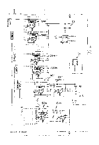
FIG. 1 illustrates a circuit structure of a (distributed control type) power
supply
controller 1 according to a first embodiment of this invention. The power
supply controller 1 is
used for a power supply system and device using a solar cell and a battery as
power sources,
particularly, for a power supply system of a space craft such as an artificial
satellite.
The power supply controller 1 is connected to a plurality of solar cells 2, a
battery 3,
and a load 4 and includes a plurality of MA modules 11, a plurality of CA
modules 12, a
capacitor bank 13, and a discharge diode 14.
The MA modules 11 each include two shunt circuits which are modularized. Shunt
circuits SM1 to SMm (m is natural number) are separately connected to
corresponding main
arrays MA I to MAm of the plurality of solar cells 2, which are used for only
power supply to the
load 4. Each of the shunt circuits includes a diode, a fuse, a power supply
circuit, an
operational amplifier, a comparator, a transistor switch, and a Zener diode.
Each of the shunt
circuits is electrically separated from the other shunt circuits and
independently operates based
on a preset threshold value.
CA modules 11 each include a shunt circuit and a charging circuit which are
modularized. The CA modules 11 are separately connected to corresponding
charge arrays
CA I to CAm of the plurality of solar cells 2, which are used for both power
supply to the load 4
and power supply to the battery 3. Respective shunt circuits SCI to SCn (n is
natural number)
included in the CA modules 11 have the same structure as the shunt circuits SM
I to SMm of the
CA 02703788 2010-04-26
MA modules 11 and each are electrically separated from the other shunt
circuits (without making
distinction between MA modules 11 and CA modules 12). Each of charging
circuits CH1 to
CHn includes a pair of transistor switches, a diode, a fuse, an operational
amplifier, a comparator,
a transistor, a Zener diode, and a switch. Each of the charging circuits is
electrically separated
5 from the other charging circuits and independently operates based on a
preset threshold value.
The shunt circuits SM1 to SMm of the MA modules 11 and the shunt circuits SC1
to
SCn of the CA modules 12 are connected common to a capacitor bank 13, detect a
voltage (bus
voltage) of the capacitor bank, and perform an on-off (switching) operation
based on a detected
voltage. When the threshold values preset for the shunt circuits SM1 to SMm
and SC1 to SCn
are made different from one another, the shunt circuits SM1 to SMm and SC1 to
SCn may be
turned on or off with different voltages from one another (for example, one by
one in order)
depending on a change (increase/decrease) in bus voltage.
The charging circuits of the CA modules 12 are connected common to the battery
3 and
perform an on-off operation based on a voltage of the battery 3. When the
threshold values
preset for the charging circuits are made different from one another, the
charging circuits may be
turned on or off with different voltages from one another (for example, one by
one in order)
depending on a change in battery voltage.
The power supply controller 1 broadly operates as follows.
When the total of the output powers of the solar cells (MAI to MAm and CA1 to
CAn)
2 exceeds the power consumption of the load 4, the plurality of MA modules 11
and the plurality
of CA modules 12 which are electrically separated stabilizes the bus voltage
to a specified
voltage and charges the battery 3 up to the specified voltage.
When the total of the output powers of the solar cells (MA1 to MAm and CA1 to
CAn)
2 is smaller than the power consumption of the load 4, power is supplied from
the battery 3 to
the load 4 through the discharge diode 14.
When the total of the output powers of the solar cells (MA! to MAm and CA! to
CAn)
2 exceeds the power consumption of the load 4 and the voltage of the capacitor
bank 13
increases, the charging circuits CHI to CHn included in the CA modules 12
connected to the
solar cells (CAI to CAn) 2 are turned on in this order (order corresponding to
CAI to CAn) to
charge the buttery 4 with excess power, to thereby stabilize the bus voltage.
When the total of
the output powers of the solar cells (MA! to MAm and CAI to CAn) 2 further
increases, the
shunt circuits SM I to SMm included in the MA modules 11 connected to the
solar cells (MA! to
MAm) 2 are turned on in this order (order corresponding to MA! to MAm) to
reduce (consume)
excess power by short circuit, to thereby stabilize the bus voltage.
CA 02703788 2010-04-26
6
When the battery 4 is charged and then the voltage thereof increases, the
charging
circuits CH1 to CHn included in the CA modules 12 are turned off in the
reversed order (order
corresponding to CAn to CA1). When the charging circuits CH1 to CHn are turned
off to
increase the excess power and then the bus voltage increases to be equal to or
larger than an
operating voltage of the shunt circuits SM1 to SMm included in the MA modules
11, the shunt
circuits SC1 to SCn included in the CA modules 12 are turned on in the
reversed order to reduce
the excess power by short circuit, to thereby stabilize the bus voltage.
According to the power supply controller 1 in this embodiment, a driver
circuit for
intensively controlling the shunt circuits and the charging circuits is not
provided and a
large-scale charging circuit (BCR) is not used, and hence (1) the shunt
circuits and the charging
circuits may be reduced in size and weight and the shunt circuits and the
charging circuits are not
affected by failure because all the circuits are separated from one another,
and (2) the shunt
circuits and the charging circuits are easily modularized and improved in
reliability.
Next, the operation of the power supply controller 1 is described in detail
with reference
to FIG. 2.
FIG. 2 is a view illustrating an operating sequence on the shunt circuits SM1
to SMm
and SC1 to SCn and the charging circuits CHI to CHn in the power supply
controller 1.
The charging circuits CHI to CHn and the shunt circuits SM1 to SMm and SC1 to
SCn
are turned on and off with a hysteresis sufficiently narrower in width than
the bus voltage. For
example, when a bus ripple standard is 500 mVpp, a hysteresis voltage of 100
mVpp to 250
mVpp is provided such that a variation in voltage becomes equal to or smaller
than the standard,
preferably 1/2 or smaller.
On-off threshold voltages for the charging circuits CHI to CHn and the shunt
circuits
SM I to SMm and SC1 to SCn are set in advance from a lower value with respect
to the bus
voltage in an order of the charging circuits CHI to CHn (BCC mode), the shunt
circuits SM I to
SMm corresponding to the solar cells (MA I to MAm) 2 (MA SHNT mode), and the
shunt
circuits SCn to SC1 corresponding to the solar cells (CA! to CAn) 2 (CA SHNT
mode).
When such setting is made, only one circuit having a (on-side or off-side)
threshold
voltage equal to the bus voltage under a power condition is turned on or off,
and hence a circuit
having a threshold voltage lower than the bus voltage is in an on state and a
circuit having a
threshold voltage higher than the bus voltage is in an off state.
Based on the setting, the charging circuits CHI to CHn are turned on and off
with a
hysteresis somewhat wider in width than the battery voltage. The on-off
threshold voltages are
set from a lower value with respect to the battery voltage in an order of the
charging circuits CHn
CA 02703788 2010-04-26
7
to CH! (CV mode). When the battery is charged to increase the battery voltage,
an
off-operation is performed in the order of the charging circuits CHn to CH1.
The operation
corresponds to a charging method of reducing the charging current stepwise as
the battery
voltage approaches the specified voltage, and hence (3) full charge may be
achieved by
large-current rapid charging without stress to the battery.
Next, the operation of the power supply controller 1 is described with
reference to FIG.
3 in addition to FIG. 2. Assume that the solar cells 2 include five main
arrays MA! to MA5 and
five charge arrays CAI to CA5 and the power supply controller 1 includes the
MA modules 11
(shunt circuits SM1 to SM5) and the CA modules 12 (shunt circuits AC! to SC5
and charging
circuits CHI to CH5) corresponding to the main arrays MA! to MA5 and the
charge arrays CA1
to CA5.
FIG. 3 is a schematic diagram illustrating the operation of the power supply
controller 1.
When power supply from the solar cells 2 to the battery 3 and the load 4 is
controlled based on
the operating sequence illustrated in FIG. 2, the operation as illustrated in
FIG. 3 is performed
based on sunshine/shade modes of the solar cells and the charging state of the
battery.
Hereinafter, the operation is described in detail.
In the shade mode, the solar cells 2 do not generate power, and hence the
power supply
controller I becomes a BAT mode in which the battery 3 is discharged. In this
case, the shunt
circuits and the charging circuits do not operate.
During an initial period in the sunshine mode, the output powers of the solar
cells 2
increase. When the output powers of the solar cells 2 exceed the load power,
the discharging of
the battery 4 is stopped and then the bus voltage starts to increase. In other
words, the power
supply controller 1 is shifted to a BCC mode.
When the output powers of the solar cells 2 further increase, the battery 4
starts to be
charged based on the bus voltage. In other words, in order to charge the
battery 4 with excess
power, the charging circuit CH1 starts to perform the on-off switching
operation. In this case,
the charging circuits CH2 to CH5 and all the shunt circuits SM I to SM5 and
SC! to SC5 are in
the off state.
After that, with the increase in output powers of the solar cells 2, the
charging circuit
CHI becomes the on state and the charging circuit CH2 starts to perform the on-
off switching
operation. Then, the charging circuit CH2 becomes the on state and the
charging circuit CH3
starts to perform the on-off switching operation. In such a manner, the
charging circuit which
performs the on-off switching operation is switched. In FIG. 3, hatching areas
exhibit the
on-off switching states of the respective circuits.
CA 02703788 2010-04-26
8
In the mode in which the charging circuits CH1 to CH5 perform the on-off
switching
operation (BCC mode), the bus voltage is controlled to a voltage higher than
the battery voltage,
and hence (4) the generated powers of the solar cells 2 are not reduced even
during the charging
of the battery.
When the output powers of the solar cells 2 further increase and then the
charging
circuit CH5 becomes the on state, the power supply controller 1 is shifted to
a shunt mode.
When the bus voltage reaches a predetermined voltage, the shunt circuit SM1
becomes the on
state through a state in which the shunt circuit SM1 performs the on-off
switching operation, and
the shunt circuit SM2 becomes an on-off switching operation state. Until this
state (MA SHNT
mode), the battery continues to be charged while all the charging circuits CH1
to CH5 are in the
on state.
After that, when the battery voltage is increased by charging, the charging
circuit CH5
is turned off and the excess power increases. In order to consume the excess
power (by short
circuit), the shunt circuit SM2 becomes the on state and the shunt circuit SM3
starts to perform
the on-off switching operation. When the battery voltage further increases,
the charging
circuits CH4 to CHI are turned off in order, and hence the circuit which
performs the on-off
switching operation is shifted in an order of the shunt circuits SM4, SM5,
SC5, and SC4.
In this case, even when the load power increases, the excess power increased
by the
turning off of the charging circuits CH5 to CHI may be supplied to the load 4.
That is, (5) the
charging power may be supplied to the load after the completion of the
charging.
When the sunshine mode is completed and the shade mode starts, the output
powers of
the solar cells 2 become smaller than the load power, and hence the bus
voltage reduces, all the
charging circuits CHI to CH5 and the shunt circuits SM1 to SM5 and SC! to SC5
are stopped,
and power is supplied from the battery 4 to the load 4 through the discharge
diode 14.
As described above, by using the distributed control type power supply
controller
according to this embodiment,
(1) the driver circuit (redundant structure) for the shunt circuits and the
charging circuit
may be omitted and reduced in size and weight.
(2) The shunt circuits and the charging circuit are electrically separated
from one
another and thus are not affected by failure, and are easily modularized and
thus easily provided
corresponding to an increase and reduction in treatment power.
(3) The charging current may be reduced stepwise with an increase in battery
voltage,
and hence the full charge may be achieved by the large-current rapid charging
without stress to
the battery.
CA 02703788 2013-07-26
74927-22
9
(4) The charging circuit may be on-off controlled to stabilize the bus voltage
in the BCC
mode, and hence the generated powers of the solar cells are not reduced even
during the charging
of the battery (SHNT mode and BCC mode).
(5) After the completion of the charging, the charging circuit may be stopped
to supply
the charging power to the load.
Next, a power supply controller according to a second embodiment of this
invention is
described with reference to FIG 4.
The power supply controller illustrated in FIG 4 is a power supply controller
in which
the discharge diode 14 illustrated in FIG 1 is replaced by a battery discharge
regulator (BDR)
unit 41. Even in the shade case (BAT mode), the stabilization may be achieved
so as to obtain
substantially almost the same bus voltage as in the sunshine case by the
action of the BDR unit
41.
As described above, this invention is described based on the embodiments.
However,
this invention is not limited to the embodiments and thus various
modifications and changes may
be made without departing from the scope of the invention.
This application claims priority from Japanese Patent Application No. 2007-
291582,
filed on November 9, 2007.