Note: Descriptions are shown in the official language in which they were submitted.
CA 02703801 2010-04-27
WO 2008/052363 PCT/CA2007/001997
1
ELECTRICAL MICROVALVE AND METHOD OF MANUFACTURING
THEREOF
FIELD OF THE INVENTION
The present invention generally relates to the field of microfluids. More
specifically, the invention relates to a microvalve for use in a microfluidic
device and to a method of manufacturing an electrical microvalve.
Background of the invention
Lab-on-a-chip and micro-total-analysis systems have been experiencing a
huge increase in interest in the biomedical and chemistry area during the
last decade. Lots of work has been done towards the development of new
technologies enabling labs to be shrunk and integrated onto single chips.
This emerging technology has proven to be very promising, and is often
referred as microfluidics. Microfluidics allows fluid flow control and mix of
fluids on chips using microchannels, in which fluids are injected. Such
chips integrate many functions on a single substrate which not only allows
an entire experiment to be built on a chip, but also allows a large amount
of parallel experiments to be performed using very small volumes of fluids
in a limited amount of time.
Microfluidic circuits require microvalves, i.e. tiny valves that are the key
building blocks for making complex microfluidics integrated circuits.
Microvalves are used to direct and pump fluids. Typically, the microvalve
is used to block the passage of the fluid in the microchannel. Many
configurations of microvalve have been investigated in prior art references.
CA 02703801 2010-04-27
WO 2008/052363 PCT/CA2007/001997
2
One of the types of microvalve is the pressure actuated flexible
microvalve which is also referred to as pneumatic valve and which is key
component of so called multilayer soft lithography (MSL) microfluidic
circuits. In such a type of microvalve, the microvalve typically includes a
flexible membrane, which is forced to block a channel by applying a
pressure thereto. Upon release of the pressure, the membrane recedes
and allows passage of the fluid in the microchannel. The pressure can be
transmitted pneumatically using gases or hydraulically using liquids.
Although effective, this technology is bulky, as it requires a separate
source of pressure for every single independent microvalve. European
Patent Application 0 845 603, filed by Xerox Corporation describes such
an air-actuated microvalve system and a method of production of such
microvalves.
Another type of microvalve also commonly known is the electrically
actuated microvalve. Such microvalve uses electricity to function.
Electrically actuated microvalves are basically composed of two
electrodes, separated by an elastomeric substance. This type of
microvalve includes two subcategories: the normally open microvalve and
the normally closed microvalve. The normally open microvalve is located
along the microchannel and requires electricity to close the microchannel,
while the normally closed microvalve is located adjacent to the
microchannel and requires electricity to open the microchannel.
International Patent Application WO 2006/044458 to University of Virginia
Patent Foundation depicts and describes an example of a normally closed
electrically actuated microvalve, while United States Patent Application
2003/0080442 to Fluidigm Corp. and United States Patent Application
2002/0109114 to California Institute of technology describe a normally-
open electrically actuated microvalve. Another interesting reference in the
art is United States Patent Application 2006/0118895 to Fluidigm Corp.,
CA 02703801 2010-04-27
WO 2008/052363 PCT/CA2007/001997
3
which describes both normally open and normally closed electrically
actuated microvalve. However, in this Fluidigm patent, the design of the
microvalve causes important stress on electrodes and elastomeric
material, which is not desirable, as it seriously reduces the lifetime of the
microvalve, necessitates high voltage (HV) for opening and closing the
valve, and slows down the actuation speed.
However, there are numerous problems with both the normally open and
the normally closed electrically actuated microvalves of the prior art. More
particularly, for the normally open electrically actuated microvalve, the
microchannel within which the sample fluid is to flow in is molded within
the elastomeric substance. Furthermore, when a conductive liquid fills the
valve, normally open valves have the drawback of stopping proper
operation under DC actuation and require high-frequency AC actuation.
Another drawback, is that the normally open electrically actuated
microvalve of the prior art, such as those described in United States
Patent Application US2002/0109114 to Fluidigm Corp. necessitates a very
high voltage of 1600V for closure which makes its use quite impractical.
As for the normally-closed electrically actuated microvalve, even though its
manufacturing is simpler than for the direct electrically actuated
microvalve, it needs to be rigid to prevent flow of liquid which makes it
difficult to actuate it, thus also requiring excessively high voltages.
More recently, direct electrical actuation of valves has been shown, which
allows high-density integration of microfluidics. However, because the
electrical fields are applied directly to conductive solutions, a DC voltage
cannot be used and high frequency AC voltages are required. In the
example published by Bansal et al., titled "A class of low voltage,
elastomer-metal 'wet' actuators for use in high density microfluidics" in Lab
on a chip volume 7, pages 164-16, the valves are 5 pm deep only, large
(600 pm in diameter) and slow (up to 5s for closing), and have not been
CA 02703801 2010-04-27
WO 2008/052363 PCT/CA2007/001997
4
used with pressurized liquids. Faster actuation and deeper channels
necessitate higher voltages, but excessive heating is likely to become an
issue. The fabrication process hitherto requires multiple difficult processing
steps and makes it difficult to produce disposable chips. Finally, the
conduits are too small to manipulate cells.
There is therefore a need for an electrical microvalve that is simpler to
manufacture, which can function over a longer period of time, which can
be actuated with lower voltages, DC current, and for which the actuation
does not depend on the composition of the sample fluid.
Summary of the invention
In accordance with an embodiment of the present invention, there is
provided a microvalve for a microchannel. The microvalve comprises first
and second electrodes. The first electrode is affixed to a portion of the
microchannel, while the second electrode is located over the
microchannel, forms a membrane demonstrating substantially no
resilience, and is substantially aligned with the first electrode. Upon
electrical actuation of the first and second electrodes, the membrane is
forced within the microchannel so as to obstruct the microchannel. A lid
adapted to support the membrane may also be provided.
In accordance with another embodiment, the present invention relates to a
method of manufacturing a microvalve. The method of the present
invention proceeds with affixing a first electrode on a microchannel. Then,
the method pursues with a step of applying a dielectric substance covering
at least a portion of the microchannel overlooking the first electrode.
Afterwards, the method includes a step of affixing a second electrode over
CA 02703801 2010-04-27
WO 2008/052363 PCT/CA2007/001997
the dielectric substance in such a manner that the second electrode is
substantially aligned with the first electrode.
In accordance with yet another embodiment, the present invention relates
to a microfluidic circuit. The microfluidic circuit comprises multiple
5 microchannels and at least one microvalve affixed to one of the multiple
microchannels. The at least one microvalve is adapted to indirectly
actuate a flexible valve which regulates a flow of fluid in another one of a
multiplicity of microchannels.
Brief description of drawings
These and other features of the present invention will become more
apparent from the following description in which reference is made to the
appended drawings wherein:
Figure 1 is a cross-sectional side view of a microvalve in a non-activated
state in accordance with an embodiment of the present invention.
Figure 2 is a cross-sectional side view of the microvalve of Figure 1 in an
activated state.
Figures 3a-e are manufacturing steps of a microchannel of the microvalve
of Figure 1.
Figures 4a-b are manufacturing steps of a second electrode of the
microvalve of Figure 1.
Figures 5a-f are manufacturing steps of a membrane in accordance with
an embodiment of the present invention.
Figures 6a-c are partial cross-sectional side views of a microchannel in
accordance with other embodiments of the present invention.
Figure 7 is a top view of the microvalve of Figure 1.
CA 02703801 2010-04-27
WO 2008/052363 PCT/CA2007/001997
6
Figure 8 is a cross-sectional side view of a microvalve in accordance with
another embodiment of the present invention.
Figure 9 is a cross-sectional side view of a microvalve having a membrane
in accordance with another embodiment of the present invention.
Figures lOa-b are perspective views of examples of uses of the
microvalve of Figure 1 in microfluidic circuit for indirect actuation of a
pneumatic valve.
Figure 11 a-b are cross-sectional views of another embodiment of the
microvalve of the present invention.
Figures 12a-b are cross-sectional views of another embodiment of the
present invention.
Figure 13 is an exploded schematic view of a microfluidic circuit in
accordance with another aspect of the present invention.
Detailed description of the invention
Miniaturization, integration and parallelization (MIP) has driven the (micro)
electronic revolution and has started to bear strongly on the life sciences,
and already revolutionized gene expression profiling with DNA microarrays
and genotyping with high throughput sequencers. The cell is the minimal
physiological functional unit, yet of extraordinary complexity as it contains
23000 genes (for humans) and many more different proteins and protein
machines. Cells have recently become an important focus of the drug
discovery processes following the increasing rate of failures of drugs in
late clinical trials or even following market introduction. High throughput
cell assays can now be performed automatically in 96 or 384 well plates
and is called high content screening (HCS) because it can provide insight
on multiple biochemical pathways. HCS is an extension of high throughput
screening (HTS) which examines individual bimolecular interactions
CA 02703801 2010-04-27
WO 2008/052363 PCT/CA2007/001997
7
outside of the cell. HCS is challenging because it requires a tight control of
environmental parameters, the delivery of multiple reagents, advanced
microscopy, and multi-parameter readouts; consequently it is expensive.
Yet HCS represents an annual market value of hundreds of millions of
USD, with a rapid growth rate of above 20 % annually. The pressure on
identifying adverse side effects of drugs early in the drug development
process fuels a rapidly rising demand for HCS in the pharmaceutical and
biotech industries. There are no intrinsic biological barriers to the further
miniaturization and parallelization of HCS and of cellular assays within
microfluidic systems, except for the lack of a microfluidic technology that
supports MIP on a large scale. For those reasons, the present invention
proposes a new microvalve, and the application of this microvalve to
microfluidic systems that renders the latter scalable, and that may be used
for cell assays and HCS. Furthermore, the present invention provides a
novel indirect control architecture where electrostatic elastomeric valves
(electrical microvalves, embedded in a control chip) regulate the pressure
of fluid in a manifold connected to flexible membrane valves which control
the flow of sample fluids. This architecture permits integration of
microelectronic integrated circuits (ICs) with microfluidics and hence
opens the door to large scale MIP of microfluidics.
With the present invention, electronic microfluidic systems will allow
performing cellular assays and HCS with greater flexibility, with much
higher throughput, and ultimately at a fraction of the cost of current
technologies. We believe that the availability of electronic microfluidic cell
chips with thousands of addressable microcompartments will transform
drug screening, cell biology and medicine in a similar manner that DNA
chips and high throughput sequencers have transformed, and are still
transforming, them.
CA 02703801 2010-04-27
WO 2008/052363 PCT/CA2007/001997
8
From a terminology standpoint, microfluidics concerns the manipulation
and transport of minute amount of liquids. Many microfluidic pumping
technologies have emerged in the last 15 years including electro osmosis,
electrophoresis, dielectrophoresis, capillary systems, MSL and droplet-
based microfluidics. Many strategies are unreliable (e.g. sensitive to the
composition of the solution, or to changes in surface chemistry, both of
which are difficult to control when using complex biological solutions) and
not suitable for integration because they depend on macroscopic
peripherals. To date microfluidics have not replaced conventional
equipments, except in few niche applications.
The present invention provides a microvalve for a microchannel, which
overcomes some of the problems known in the art. Furthermore, the
microvalve of the present invention is composed of elements that are
affixed to the microchannel and surrounding surface. Also, the present
invention provides for a microvalve which reduces the need for high
actuation voltages, is amenable to large-scale integration, and is much
more resistant over time due to its intrinsic design. Finally, the present
invention provides and uses a microvalve, which relies on a membrane
demonstrating substantially no resilience to indirectly actuate a flexible
valve controlling sample fluid flow.
A general embodiment of the present invention will now be described.
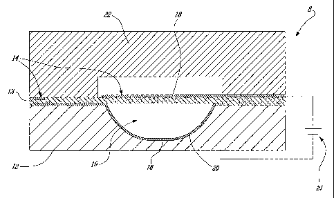
Figure 1 depicts a microvalve 8 in accordance with the present invention,
in a non-activated state. The microvalve 8 is to be used for
obstructing/closing/opening a flow of fluid (not shown) in a microchannel
10. The term "fluid" is used throughout the description so as to include
either liquid or gaseous substances, or a combination thereof. The
microchannel is manufactured in a base 12, which for example may
consist of glass or ceramic or an elastomer or any other material of similar
CA 02703801 2010-04-27
WO 2008/052363 PCT/CA2007/001997
9
properties. The microchannel 10 has a longitudinal opening exposing a
portion or the entire channel 10. The microvalve includes a first electrode
20, a second electrode 18 and a dielectric substance 13. The first
electrode is located alongside a section 16 of the microchannel 10. The
first electrode 20 could be located in such a manner that it is perpendicular
with the microchannel or at an angle therewith, depending of an angle
required for the microvalve across the microchannel. The second
electrode 18 forms a membrane demonstrating substantially no resilience.
The dielectric substance is located in such a manner that it covers at least
a longitudinal portion of the microchannel opening and covers a complete
cross-sectional portion of the microchannel. The dielectric substance may
consist of a solid or semi-solid material. The dielectric substance may for
example be composed of an elastic or elastomeric material, such as a
membrane of polydimethylsiloxane, PolyMethyl MethAcrylate (PMMA),
Polycarbonate, photoresists, SU-8, parylene, Si02, Si3N4 or any other
material having similar electrical and elastic properties. More particularly,
in an embodiment of the present invention, the dielectric substance
together with electrode 2 forms the membrane demonstrating substantially
no resilience 14 that may have a thickness of less than 10 m. The
dielectric substance is preferably extremely flexible, and therefore the
membrane 14 requires small voltages between the first and second
electrodes for being forced onto the first electrode. The second electrode
18 is either located over, within or underneath the dielectric substance 14,
and is substantially aligned with the first electrode 20 (shown concurrently
on Figures 1 and 9). The first and second electrodes 20 and 18 are
composed of an electrically conducting material, for example Al, Cr, Ti, Au,
carbon, a conductive polymer or any combination thereof or any other
suitable material. In a preferable manner, the second electrode 18 is
composed of an electrically conducting material that also tolerates certain
flexibility so as to be durable when operating the microvalve, such as a
conductive elastomer. Finally, a cover lid 22 may be provided over the
CA 02703801 2010-04-27
WO 2008/052363 PCT/CA2007/001997
second electrode 18 so as to support the membrane 14 when pressure is
applied to the channel.
Reference is now made concurrently to Figures 1 and 2, where Figure 2
5 shows the microvalve 8 in an activated position. To operate the
microvalve 8, the first and second electrodes 20 and 18 are electrically
connected to an electrical source 21. In function, the electrical source 21
applies an electrical force on the first and the second electrodes 20 and
18, which draw the second electrode 18 nearer to the first electrode 20,
10 thus substantially, obstructing/closing the microchannel. Thus, when the
microvalve 8 is not actuated, the microchannel 10 is open and fluid can
freely flow therein. However, when the microvalve is actuated, the
microchannel 10 is substantially obstructed/closed and fluid cannot freely
flow there through.
When the membrane 14 is forced against the microchannel, it may not
spring back to the open position by itself because of adhesion forces
between the membrane and the microchannel surface and because of the
lack of resilience of the membrane 14. The application of a pressure to the
microchannel will however detach the membrane 14 from the
microchannel surface, and press it against the cover lid and thereby open
the microchannel. The use of membranes such as described may appear
unpractical because a sample microchannel may remain closed for lack of
pressure. However, because of indirect actuation, as described below, the
use of membranes 14 becomes practical, and offers a surprisingly
attractive solution to make electrical valves. In addition, the microvalve
surface can be made rough or ruguous so as to reduce the adhesion
forces between the membrane 14 and the microchannel surface.
CA 02703801 2010-04-27
WO 2008/052363 PCT/CA2007/001997
11
It will be apparent to those skilled in the art that due to its design and the
selected materials, the microvalve of the present invention requires from
the electrical source 21 a lower electrical voltage than microvalves of the
prior art.
Manufacturing process
In general, the method of manufacturing some aspects of the microvalve
of the present invention consists of affixing the first electrode 20 on a
portion of the surface 16 of the microchannel 10, applying the dielectric
substance 13 in such a manner that it covers at least a portion of the
microchannel 10 while overlapping the first electrode 20, and affixing the
second electrode 18 over the dielectric substance 13.
More particularly, Figures 3a to 3e depict a possible method for
manufacturing the microchannel 10 over the base 12. The process
consists of coating a glass substrate 12, or a similar material, with metal
80 and spin coating a photosensitive material 82 thereon. Then, the base
12 is exposed to ultra-violet light through a photolithographic mask 84, so
as to expose only the desired region(s). The photosensitive part 82
exposed to ultra-violet light is afterwards developed (i.e. dissolved in the
appropriate chemicals). Then, the metal 80 is etched in order to expose
the base 12. Finally, the microchannel 10 is etched in the base 12 made of
for example borosilicate type glass; using a hydrofluoric acid (HF) based
wet chemical solution. The solution may be made of HF, ammonium
fluoride (NH4F) and hydrochloric acid (HCI). More particularly, in Figure
3a, the base 12 is coated with a metal 80 and a spin coated photoresist 82
on top. The microchannel 10 is selectively etched in the base 12 by
exposing the photosensitive material 82 to UV light 83 through the
photolithographic mask 84. The sidewall angles of the microchannel 10
CA 02703801 2010-04-27
WO 2008/052363 PCT/CA2007/001997
12
are controlled by carefully tuning the combination between the bath
temperature, agitation and chemical concentration and the hard mask 80
resistance. A very resistant hard mask will produce very vertical sidewalls
whereas a hard mask that slowly lifts off during etching will produce
smoother sidewalls. Having smooth sidewalls prevents any discontinuities
in the metal of the first electrode 20 when it is subsequently deposited on
the portion 16 of the microchannel. Typically, a microchannel is between
and 150 pm wide and 1 to 30 pm deep. It is possible to round off edges
24 (shown on Figure 2 and Figure 6a). Rounded edges 24, as shown in
10 Figure 6b-c, decrease the stress induced in the second electrode 18 when
it is activated and tries to conform to the first electrode 20. Rounded edges
24 also allow the dielectric substance 13 to better follow the profile of the
microchannel 10 and therefore seal better the microchannel 10.
Reference is now made to Figures 4a to 4b, which depict an exemplary
method of manufacturing the first electrode 20. The first electrode 20 is
fabricated using standard lithographic and metal etching techniques. The
electrode is composed of an electrical conducting material. The first
electrode 20 is deposited on the portion 16 of the microchannel and then
the photosensitive material 82 is used to coat the first electrode 20 using
for example a multicoat technique to improve the coverage near the edges
24 of the microchannel 10. This also helps in preventing discontinuities in
the material of the first electrode 20. The first electrode 20 may be
manufactured for example of any of the following metals: Al, Cr, Ti, Au,
Cu, and any combination thereof or any other suitable material. Typically,
the first electrode 20 is between 50 - 500 nm thick. In a preferable
manner, the first electrode 20 is further electrically isolated with a layer
of
silicon oxide, silicon nitride, tantalum oxide, any combination thereof or
any other suitable material that can be deposited by sputtering, chemical
vapor deposition, or spin-on techniques.
CA 02703801 2010-04-27
WO 2008/052363 PCT/CA2007/001997
13
Reference is now made to Figures 5a to 5f, which depict an exemplary
method of manufacturing the dielectric substance 13, and the remaining
steps of the manufacturing of the microvalve 8. To create the dielectric
substance 13, a material such as for example polydimethylsiloxane
(PDMS) is first poured on a thin plastic film 85 that has received an
antiadhesion treatment (either plasma or liquid) and spincoated such as to
create a thin PDMS membrane. The thin plastic film 85 may be held on a
silicon wafer. The thickness of the spun-on PDMS material 13 can be
finely tuned to be within 500 nm to 30 pm, preferably about 3 pm. The
plastic film PDMS membrane assembly is then flipped and transferred on
the base 12 (Fig 5c), containing the microchannel 10 and the first
electrode 20. During this step, the plastic film PDMS membrane assembly,
the microchannel and the first electrode 20 are then exposed to oxygen
plasma 87 to activate their surfaces prior to bonding, and then
permanently bonded. The adhesion of the PDMS membrane 13 onto the
base of the microchannel 10 can be improved by a soft bake of several
(30 to 60) minutes in an oven at a temperature of about 70 C. The plastic
film 85 is eventually pealed off easily, Fig. 5d, since the bonding strength
is higher at the membrane-base interface, thus leaving the dielectric
substance 13.
The second electrode 18 is fabricated directly on the dielectric substance
13 by first depositing a thin metal layer 86 of electrode material such as
Cr/Au as shown in Figure 5e. Approximately 1 to 20nm may be deposited.
The metal layer 86 is patterned using lithography and wet etching. Once
the second electrode 18 is deposited on the dielectric substance 13, the
lid 22, with cavities matching the microvalve 10 location, is bonded to the
base 12 using oxygen plasma surface activation. The base 12 and the lid
22 may be made of for example PDMS or glass. Alternatively, it may be
CA 02703801 2010-04-27
WO 2008/052363 PCT/CA2007/001997
14
possible to replace the second electrode 18 by a conductive polymer or
elastomer electrode.
In another embodiment of the present method of manufacturing, after step
4b where the metallic bottom electrode is etched using a wet chemical
solution, a dielectric insulation thin layer is deposited via sputtering,
evaporation or chemical vapor deposition. The layer could be silicon
dioxide (Si02), silicon nitride (Si3N4), tantalum pentoxide (Ta205) or any
highly resistive material exhibiting a high breakdown voltage. Steps 5a to
5b are similar as previously described. Before step 5c, there is an
additional step which consists in patterning an electrode on the elastic
substance. This electrode is the second electrode of the microvalve. In
order to increase adhesion of metal onto the substance, several strategies
can be used: a metallic adhesion layer that could be chromium or titanium
can be added, or a self assembled monolayer silane or any chemicals that
is susceptible to increase metallic adhesion could also be used. Once the
electrode is patterned, the substance and the base are oxygen plasma
treated and bonded together (step 5c). The bonding strength is increased
with a 30 to 60 min cured in an oven at 70 C. During step 5d, the plastic
film 85 is peeled off easily since the bonding strength is higher at the
membrane-base interface, thus leaving the dielectric substance 13 and
the second electrode 18 attached underneath.
For the embodiment where the second electrode is within the dielectric
substance 13, the manufacturing process requires an additional step after
patterning the second electrode: another elastic substance that could be
PDMS is poured and spin coated on the electrode 18 and cured at 70 C
for 30 to 60 minutes. The process then continues with step 5c.
CA 02703801 2010-04-27
WO 2008/052363 PCT/CA2007/001997
Method of manufacture of the microfluidic circuit
In the context of the prototype, hereinafter described in greater details, a
prototype of the electrical microvalve has been manufactured by
5 transferring 10-micrometer-thick membranes spanning a channel that is -
12 pm deep and 100 pm wide (shown on Figure 13), and demonstrated
electrostatic deflection of the membrane under applied voltage. 2nd
generation electrical microvalves with membranes only 3 pm thick and
arranged as arrays in a micro-electro pneumatic chip were also
10 manufactured. A new simplified fabrication process that allows making
each layer on a wafer was developed, to assemble the chips by stacking
different layers, thus greatly simplifying the process. An enhanced
sacrificial layer release pioneered by Genolet et al. at IBM which allows
the quick release of large structures on a wafer scale was implemented. It
15 was noticed that the micrometer-thin PDMS membranes are very fragile,
and can easily be ruptured during fabrication, which can be avoided using
this release process.
An important challenge is the fabrication of thin PDMS membranes with
the high yield necessary for large scale integration. The current fabrication
method for making thin valves is based on spin-coating 3-5% PDMS
diluted in toluene and patterning Au by wet etching on top of it to define
the electrodes. There are many parameters that may be changed, such as
the solvents used for spinning or even the supporting polymer. Indeed, for
a valve with a low aspect ratio of 1:50 (current design) the strain produced
by closing the valve is very small (only 0.12 percent assuming a circular
cross section for the channel), which can be achieved using a wide range
of materials, including polymers such as SU-8 or PMMA (both of which
can be coated down to nanometer thicknesses), or dielectric films coated
by evaporation or sputtering. With this geometry, the electrical material
CA 02703801 2010-04-27
WO 2008/052363 PCT/CA2007/001997
16
alone may form the membrane 14, whereas the dielectric substance 13 is
attached to the first electrode.
Reduction of stress
Reference is now made to Figures 6a-6c, which depict partial cross-
sectional side views of the actuated microvalve 8 in the microchannel 10 in
accordance with other embodiments of the present invention. More
particularly, Figure 6a illustrates that it is preferable, to reduce stress on
the microvalve 8, that the microchannel 10 be provided with edges 24 that
are rounded. At the edges of the channel, the pressure of the closing of
the microvalve causes a large strain (stretching) whereas at the bottom of
the channel, it causes the first electrode to be compressed. Such a
situation is not preferred, as excessive stretching can tear the first and the
second electrodes apart, thus reducing the lifetime of the valve. Figure 6b
shows the actuated microvalve in the microchannel 10, wherein the
sharpness of the edges 24 of the microchannel 10 have been reduced,
and the remaining stress area for the microvalve is located at the bottom
of the microchannel 10. Figure 6c depicts a preferred design for the
microchannel. The preferred design includes rounded edges and reduced
sidewall angle so as to totally reduce the stress on the microvalve at both
the microchannel edges and at the bottom thereof. This design has
another interesting advantage: it reduces the electrical tension required
from the electrical source to close the microvalve.
Another way to reduce stress is to provide second electrodes that are
longer than the width of the microchannel. The electrodes may take the
shape that is rectangular, spiral, sinusoidal or saw-tooth shaped. This
improvement reduces the stress on the electrode and reduces chances of
tearing the membrane 14.
CA 02703801 2010-04-27
WO 2008/052363 PCT/CA2007/001997
17
Particularities of the second electrode
Reference is now made to Figure 7, which depicts a top view of the
microvalve 8 installed on the microchannel 10 and ready to operate. In
that view, the first electrode 20 is at the bottom of the microvalve, the
second electrode 18 is connected to a pad 26, for future wire bonding or
probing or contacting, through an access line 28. The access line 28 is
routed such as to follow a path of minimum strain to reach the second
electrode 18. It should be noted that as the deflection is at its greatest
where the pressure created by the first and second electrodes is the
greatest, it is advantageous to locate the access line 28 in such a manner
that it is outside of the deflection area, thus reducing the resulting strain
at
the edge of the microchannel and consequently on the access line itself.
Because the second electrode 18 needs to be flexible as it is stretched
when the microvalve 8 is activated, the second electrode 18 may be
rectangular, round, circular, spiral shaped, saw-teeth shaped, or sinusoidal
shaped. The ratio between electrode and non-electrode area can be
varied. For example, the ratio could be as low as at least 1:20, 1:50 or
even at least 1:100. Such designs help reduce tearing of the second
electrode 18 and help in increasing its lifetime.
Fig. 7 shows an example of a long second electrode 18 crossing a
narrower first electrode 20. The second electrode 18 and the dielectric
layer 13 (shown in cross-section in Fig. 1) together form a two-layer
structure that is more resilient than the dielectric layer 13 alone. At the
edge of the first electrode 20 located within the microchannel 10 within the
microvalve cross-section, there may be a strong strain on the dielectric
material 13 when the second electrode 18 is actuated and closed whereas
the dielectric layer 13 not overlapping with the second electrode 18 is
pressed against the lid (Number 22 with reference to figure 1) by the
pressurized fluid in the microchannel 10. A way to reduce stress on the
CA 02703801 2010-04-27
WO 2008/052363 PCT/CA2007/001997
18
dielectric layer 13 within the microchannel cross-section is to make the
second electrode 18 extend longitudinally in the microchannel over a
distance that is greater than the width of the first electrode 20, so that the
strain upon deflection of the membrane 14 is carried both by the second
electrode 18 material and the dielectric material 13 of electrode 18.
Microvalve with recesses
To prevent the membrane 14 from deflecting upwards under pressure
caused by fluid flowing in the microchannel 10, or inwards under its own
weight, the lid 22 may be provided with posts or walls 32, as shown in
Figure 8. The posts or walls stop the membrane 14 from deflecting
upwards under pressure, and the membrane 14 can stick to the posts or
walls 32, which prevent it from deflecting into the microchannel 10. The
recesses allow opening and closing the microvalve 8 rapidly because they
provide enough volume for air to fill and move away when the microvalve
is closed and opened, respectively. Without recesses, the microvalve 8
may still open, but more slowly because the void that is then formed
creates a vacuum that has to be filled by gas drained from the surrounding
material of the cover lid. The gas reservoir afforded by the recesses allows
rapid opening and closing of the microvalve. In addition, the surface of the
recesses can be roughened so as to reduce the adhesion between the
membrane 14 and the recesses. Examples of typical width of the posts or
walls can be 1 - 100 pm, the gap between the posts or walls 1 - 100 pm,
and the length of the walls can be 20 um to 1 mm. Examples of roughness
are 1 nm - 2 pm in length and 1 nm to 10 pm in height.
CA 02703801 2010-04-27
WO 2008/052363 PCT/CA2007/001997
19
Use of microvalves for pneumatic and hydraulic applications
In prior art MSL chips, the pressure in a pneumatic or hydraulic control line
deflects a thin elastomeric membrane - serving as a valve - into a sample
channel and closes and opens it. Such microfluidic architecture and
variants of it have been successfully used for a variety of applications
including pumping, protein crystallization, immunoassays, quantitative
PCR, bacterial culture, etc. The success of this approach is rooted in the
versatility of the technology, in the low cost of the chips made out of
polydimethylsiloxane (PDMS), and in the ease with which it can be
fabricated and operated using a computer. Large-scale parallelization is
accessible with MSL using a dual control layer (a pneumatic multiplexer
controls the pressure in pneumatic lines which deflect membranes into
samples channels and thereby control sample flow) similar to RAM
architecture. Thus, n chambers can be addressed using 2 Iog2 n
pneumatic or hydraulic control lines only, e.g. 1024 chambers using 20
control lines. One drawback is that this architecture is organized around
few inlets and outlets, and large volumes of samples are expended in the
maze of channels. But significantly, the control depends on macroscopic
solenoid valves that need to be connected with macroscopic pins to the
chip. Only a single MSL chip can be operated at one time.
Reference is now made to Figures 10 a-b, which depict a perspective view
of an application of the microvalve of Figure 1 respectively in accordance
with two embodiments of the present invention. The first embodiment
depicted in Figure 10 a relates to a normally open microvalve and the
embodiment of Figure 10 b relates to a normally closed microvalve.
Those embodiments are also called microfluidic circuit with indirect
electrostatic actuation.
CA 02703801 2010-04-27
WO 2008/052363 PCT/CA2007/001997
In this particular application, a base 212 may contain many microchannels
210 (of which only one is shown for clarity purposes). The microchannel
210 is adapted to receive fluid. The microchannel 210 is covered with a
flexible membrane 255, which is adapted to obstruct/close the
5 microchannel 210 upon pressure actuation 249 in a partially superposed
channel 250. The flexible membrane 255 can be with or without resilient
force, depending on the application to be implemented. As in some
instances, the microchannel 210 may be used to carry sample fluids with
electrical conductivity; it is preferable to use the electrical microvalve of
the
10 present invention so as to indirectly actuate the flexible valve so as to
not
affect the operation of the electrical valve by the conductive fluids.
For such applications, the present invention, shown on Figures lOa-b and
Figure 13, proposes an indirect valving architecture where the electrical
15 microvalve is embedded in a micro-electro pneumatic or micro-electro
hydraulic chip and operated using HV ICs, and can replace the external
solenoid valves in the multiplexed MSL architecture described previously,
by controlling the pressure inlets, or by replacing the multiplexing control
valves, or by directly controlling the pressure acting on the sample control
20 valves, or a combination of these schemes.
More particularly, in the case of Figure 10a, when the microvalve 201 is
not actuated, the pressurized fluid circulates in the microchannel 250
without forcing the flexible membrane 255 in the microchannel 210, thus
allowing passage of sample fluid therein. However, upon actuation of the
microvalve 201, passage of fluid is obstructed in the microchannel 250,
which results in the flexible membrane 255, to take expansion in the
microchannel 210, thereby obstructing the latter.
In the embodiment shown on Figure 10b, an alternate indirect actuation is
depicted. In that alternate embodiment, the microchannel 250 is closed at
CA 02703801 2010-04-27
WO 2008/052363 PCT/CA2007/001997
21
an extremity thereof. When the microvalve 201 is not actuated passage of
fluid in the microchannel 250 is permitted and because the end of the
microchannel is closed, the pressurized fluid forces the flexible membrane
255 in the microchannel 210 thus obstructing passage of sample fluid
therein. However, when the microvalve 201 is actuated, the passage of
gas is blocked, and the pressurized air dissipates in the flexible membrane
255, and in the surrounding material 214, which removes the pressure on
the flexible membrane 255 which frees the microchannel 210 allowing
passage of sample fluid therein. In another implementation, a small
drainage channel may be formed in the extremity of the microchannel so
that when the microvalve is actuated, the passage of fluid is blocked, and
the pressurized gas or liquid can dissipate through the drainage channel,
which removed the pressure on the flexible membrane 255 as described
above.
The approach of the present invention is thus compatible with large scale
MIP and with cell culture, is low cost, and can regulate pressures of at
least 50 kPa, and thus overcomes all of the above mentioned
shortcomings. A single, unregulated pressure line connected to the micro-
electro pneumatic chip is sufficient because an air manifold distributes the
gas within the chip, and directs it to different branches connected to a
disposable MSL chip. The pressure in each branch acts on a pneumatic
valve in an MSL chip, but is regulated with an electrical microvalve 201
under the control of the HV ICs. Electrical microvalves 201 in the micro-
electro pneumatic chip operate independently of the sample fluid
composition, and small electrical microvalves can be used to actuate
much larger pneumatic valves, or even multiple valves connected
together. The electrical microvalve 201 exploits the elastic properties of
ultra thin films on the dielectric membrane, such as ultra thin Au films
which can be strained up to 20% without rupture, well beyond the current
requirements.
CA 02703801 2010-04-27
WO 2008/052363 PCT/CA2007/001997
22
Using this indirect actuation scheme, low aspect ratio channels with thin,
membranes that collapse (and thus eliminate the mechanical resistance
opposing the closing of the valve) can be used. These pneumatic valves
are functional because in use the fluid pressure opens them up. Lids
covering the electrical microvalve 201 (Figure 13) provide support and
prevent excessive deflection and rupture of the membrane under the fluid
pressure, and ensures that the two electrodes stay within the electrostatic
actuation range. The 100 x 100 square micrometers membranes with a
1 00-nm-Si02 layer form a capacitance of - 4 nF when closed. Using 300V
with a 2-pm-gap, a pressure of - 200 kPa can be regulated. With these
parameters, 180 pJ are stored in a capacitance of an electrical microvalve
that is closed, which can easily be driven with the HV ICs. By working at
lower pressure, the voltage may be reduced, or the depth of the conduit
increased (the force scales with the inverse of the square of the gap). By
reducing the area of the electrical microvalve, or the voltage, the energy
can be reduced (and the electrical energy "recycled" by using smart
electronics). This configuration is not compatible with direct valving for the
reasons mentioned above and because such a shallow channel creates
excessive resistance to sample fluid flow (but not to actuation fluid flow
that requires only very small volumes).
Figure 11 a shows a microvalve that features two second electrodes 18a
and 18b and that is preferentially used for hydraulic applications. The
microvalve is used to actuate a flexible valve located downstream of
opening 301. Microvalve 18a is actuated first and closes channel 10.
Microvalve 18b is actuated thereafter and displaces the fluid between
electrodes 18a and 18b, which creates a pressure in the channel 10 and
in the opening 301 and thus displaces the flexible valve to close a
microchannel containing sample fluid.
CA 02703801 2010-04-27
WO 2008/052363 PCT/CA2007/001997
23
Figure 11 b shows another embodiment of a hydraulic microvalve. Here the
geometry of channel 10 is such as the width is wider on the edge 305 of
the electrode 18 and narrower on the edge 304. Thus, upon application of
electrical force, the valve initially closes on the edge 305. Once it is
closed
on the edge 305, the closure of the other areas of the valve will contribute
to increase the pressure downstream of the valve and in the opening 301
and on the flexible membrane that interrupts a flow of sample fluid. It will
be apparent to the skilled in the art, that instead of a V-shaped width, a
channel with variable depth may be used or an electrode with areas
without electrode material (The larger the area without electrode material,
the smaller the electric force and the later the electrode will close). For
example if the non-electrode are is higher on the edge 306, the edge 305
will close faster as described above. Different driving voltages may be
used to increase the time lag between the closure between the edge 305
and the edge 306 of the electrode.
Figure 13 shows an electronic microfluidic chip in accordance with another
aspect of the present invention. An exploded view of a micro-electro
pneumatic chip with electrical microvalves and of a MSL chip with
pneumatic membrane valves is shown. . The electrical microvalve
comprises two electrodes, one coated atop of the elastomeric membrane
and one at the bottom of the microconduit connected to a power supply.
Although throughout the present specification, the expression microfluidic
circuit is being used, it is meant to also include microfluidic chips, and all
other similar expressions commonly used in the field.
CA 02703801 2010-04-27
WO 2008/052363 PCT/CA2007/001997
24
Architectures
Another example of application of the microfluidic circuit with the
microvalve of the present invention is to realize an architecture that can be
interfaced directly with microelectronic chips and that is therefore scalable.
As the microvalve of the present invention can be closed by applying a
voltage, it can therefore be directly controlled using electronic chips. Thus,
using a computer, complex fluidic operations can be programmed and
using a microelectronic chip the microvalves in the microfluidic circuit
actuated accordingly. This concept hinges on the large-scale integration of
microelectronic chips and allows accelerating the integration and
parallelization of microfluidics.
Using the microvalve of the present invention renders microfluidic circuits
extraordinarily versatile and ideally suited for performing complex
experimental protocols in parallel with high throughput while economizing
reagents and reducing costs. Such microfluidic circuits could transform
high cell biology--specifically high throughput cell assay--and medicine
akin to the way that DNA chips and high throughput sequencers have
transformed, and are still transforming, them.
An additional aspect of the present invention lies in the overall concept
and architecture for integrated electronic microfluidic systems with two
fluidic chips - a disposable MSL chip reversibly connected to an micro-
electro pneumatic or a micro-electro-hydraulic chip with electrical
microvalve - controlled using HV ICs, and in the technical details
supporting their realization. More particularly, the following aspects are of
interest: the indirect valving concept using a micropneumatic circuit (with a
gas manifold) or micro hydraulic circuit (with a liquid manifold) controlled
by electrical microvalve which is a significant advance because it acts as a
CA 02703801 2010-04-27
WO 2008/052363 PCT/CA2007/001997
bridge between microelectronic ICs and microfluidics, thus paving the way
for large scale MIP of microfluidics; the concept and design of the flimsy,
non-self-supporting electrical microvalve formed across low aspect ratio
conduits; and finally, the simplified fabrication process to make these
5 valves.
Other microvalve combinations examples
Reference is now made to Figures 12a-b, which depict a cross-sectional
10 view of another indirect pneumatic actuation embodiment of the present
invention. In this embodiment, the use of a three-electrode electrical
microvalve for pneumatic network is described. The pneumatic network is
meant to actuate microvalves in a microfluidic network.
15 On Figures 12a-b, the three electrodes can be named electrodes 1, 2 and
3 from the bottom one to the top one. This embodiment represents a
"latch" valve. The two generic electrodes (no 1 and 3) are kept at potential
1 and potential 2, whereas electrode 2 can be addressed with potential 3,
which can vary between potential 1 and 2. In an inactive state, the value of
20 electrode 2 is in between so that there is an electrical field between
electrodes 1 and 2 and between electrodes 2 and 3. However, if electrode
2 is closing the channel (Figure 12a) the distance to electrode 1 is much
shorter and hence the electrical field and the force. Thus it remains in that
position. Conversely, if electrode 2 is open (Figure 12b) then it is much
25 closer to electrode 3, and hence the electric field between 2 and 3 is much
higher than between 2 and 1 and thus electrode 2 is stuck to the ceiling.
To actuate electrode 2, a brief pulse at the potential of the nearest
electrode will disrupt the electrical field so that it is attracted to the
remotely located electrode. For example if it is located on electrode 1, by
setting the potential of electrode 2 equal to electrode 1, the electrical
field
CA 02703801 2010-04-27
WO 2008/052363 PCT/CA2007/001997
26
will be strongest between 1 and 3, and thus the valve will be opened and
electrode 1 pressed against electrode 3. By setting briefly the potential of
electrode 2 at the value of potential 3, the valve will be closed by the same
mechanism. Thus by keeping the electrode 2 at an intermediate potential,
it will just remain to whichever electrode it is pressed upon. This
configuration can therefore serve as both a normally open valve and a
normally closed valve, depending on the need of the moment. This greatly
facilitates actuation of an array of valves where some valves need to be
closed most of the time and some other valves open most of the time.
Only electrodes 2 need individual addressing, which greatly facilitates
integration. Additionally, electrodes 2 could be addressed individually or
as groups.
Prototype
In the context of the present invention, a prototype electronic microfluidic
system using the teachings of the present invention has been built and
used for automated cell culture and assays. The following phases were
followed in the development of the prototype:
Phase 1: Develop electrostatic elastomeric valves (electrical microvalve),
also called microvalve, for regulating the pressure in a manifold embedded
in a micro-electro pneumatic (MEP) chip; an electrical interface and
connections to a sample chip;
Phase 2: Design and microfabricate a multilayer soft lithography (MSL)
sample chip with pneumatic membrane valves suitable for cell culture. The
MSL chip was disposable and could be connected to the MEP chip;
Phase 3: Integration of high voltage (HV) ICs, and the above mentioned
MEP and MSL chips on a custom designed PCB connected to a computer
with a control program that is used to program the HV ICs. The HV ICs
control the electrical microvalves which control the membrane valves in
the MSL chip; and
CA 02703801 2010-04-27
WO 2008/052363 PCT/CA2007/001997
27
Phase 4: Testing of the electronic microfluidic chips and demonstration of
complex fluidic operations with the delivery of cells to the microfluidic
compartments, and assess the merit of electronic microfluidics for HCS.
Phase 1 consisted of building MEP chips with electrical microvalve. The
major task was the fabrication of a MEP chip with at least 40 independent
electrical microvalves that could regulate at least 0.5 bar using 300 V. The
current test chips microfabricated were 25 x 25 mm2 in size, feature sets
of 32 electrical microvalves with variable dimensions and a standardized
interface with 168 electrical connections by patterning Au on PDMS (which
forms excellent electrical contacts13). The thickness of the membrane and
the depth of the pneumatic channel were adjusted during fabrication.
Molding processes that were developed previously were used to define
(vertical) via in both the MEP and MSL chips and which served as
pneumatic connections between the electrical microvalves and the
membrane valves of the MSL chip. The design of the electrical microvalve
and pressure manifold were optimized for efficiency and the fabrication
process for higher yield, which necessitated continuous efforts and careful
processing of the chips in the clean rooms. Next, the 2nd generation MEP
chip were designed and microfabricated. The current processes was
further refined for increasing the yield and different surface chemical
treatments based on silanes and thiols were used to control adhesion
depending on the requirements.
Phase 2 consisted of building an MSL chip suitable for cell culture, and
interconnection via matching the ones of the MEP chip. MSL is a well-
established technology, and published design rules were followed to make
an MSL chip. Synthesis of a set of universal requirements of HCS and
cellular assays were elaborated to guide the design of the MSL chip. The
fluidic network architecture was defined by improving on the functions and
features of published MSL chips and applications. Channel dimensions of
CA 02703801 2010-04-27
WO 2008/052363 PCT/CA2007/001997
28
- 50 pm width, - 20 pm depth, and cell culture micro compartments - 400
pm wide (with support posts) are foreseen. The MEP chip and MSL chips
were aligned using a homemade alignment tool and reversibly clamped
together on the PCB. For small chips, mechanical clamping was used,
whereas for larger chips a vacuum-based clamping using a manifold is
being foreseen.
Phase 3 consisted of building an electronic microfluidic system comprising
a custom-designed PCB, the MEP and MSL chips developed in phase 1
and 2, five HV lCs bonded to a glass carrier and connected to the PCB,
and a computer connection. Programming in LabviewTM was developed for
controlling the 5 HV IC chips each featuring 10 programmable HV control
lines operating at up to 300 V and supporting a load of 2 mA.
Phase 4 more particularly consisted of testing the electronic microfluidic
system and demonstrating complex fluidic operations and delivery of cells
to the micro compartments. Using a pressure regulator, the manifold was
pressurized, as well as the sample containers. Although a single pressure
line would be sufficient, additional pressure lines were used in this
prototype to simplify operation. The PCB was mounted on an inverted
microscope equipped with an incubation chamber enabling both
observation and cultivation of cells in the electronic microfluidic system.
The system was qualified, the merit of the technology assessed and an
analysis of the shortcomings provide and improvements proposed. This
evaluation was performed with respect to live cell assays and HCS.
The present invention has been described with regard to preferred
embodiments. The description as much as the drawings were intended to
help the understanding of the invention, rather than to limit its scope. It
will
be apparent to one skilled in the art that various modifications may be
made to the invention without departing from the scope of the invention as
CA 02703801 2010-04-27
WO 2008/052363 PCT/CA2007/001997
29
described herein, and such modifications are intended to be covered by
the present description.