Note: Descriptions are shown in the official language in which they were submitted.
CA 02705969 2010-06-04
TITLE: OPTICAL RECEIVER WITH MONOLITHICALLY INTEGRATED PHOTO
DETECTOR
FIELD
[0001] Embodiments of the present invention relate generally to optical
receivers,
and more particularly to compensated optical receivers having monolithically
integrated
photodetectors.
INTRODUCTION
[0002] Optical receivers can be utilized in various different applications,
such as
local-area networks (LAN) and fiber-to-the-home (FTTH) interconnects, as well
as in
interfaces for optical storage systems, such as CD-ROM, DVD and Blu-Ray Disc.
In these
applications, a photodetector can be used to convert incoming optical data
signals into
electrical detection signals for further processing, such as decoding,
amplification,
equalization, and compensation. In some types of optical data systems, the
photodetector
can be housed in a separate chip or as a standalone component and connected to
other
signal processing elements in the optical data system using bond wires or
other
connections. Although this solution allows for the use of high quality and
high data rate
photodetectors, extra overhead and assembly cost associated with the
photodetector, as
well as electrostatic discharge (ESD) problems and other parasitics associated
with the
bond wires can be some of the resulting drawbacks.
[0003] In other optical data systems, the photodetector can be monolithically
integrated with other signal processing components on a single semiconductor
substrate
and implemented, for example, using standard integrated circuit (IC)
technologies, such as
complementary metal oxide semiconductor (CMOS), Silicon Germanium (SiGe) and
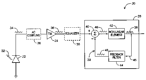
mixed
bipolar CMOS (BiCMOS) processes. Light detection in CMOS technology can be
performed using a pn junction fabricated in the substrate, for example by
appropriate
doping of the semiconductor, and operated with a reverse bias voltage to
create a depletion
region. When an incoming optical data signal is received at the photodetector,
electron-hole
pairs (i.e., charge carriers) generated by the incident photons can be
collected in an anode
coupled to the depletion region for intensity measurement and optional post-
detection
-1-
CA 02705969 2010-06-04
processing in order to reconstruct the transmitted optical data signal.
Because the
photodetector is monolithically integrated on the semiconductor, use of bond
wires is
minimized and overhead is reduced. Other advantages common to integrated
devices,
such as low cost and manufacturability, are also realized.
SUMMARY
[0004] In accordance with one aspect, there is provided an optical receiver
comprising a photodetector, an amplifier and a signal compensation circuit.
The
photodetector can generate a detection signal representative of an optical
data signal
received at the photodetector and having a distortion component caused by an
operating
characteristic of the photodetector. The amplifier can amplify the detection
signal to
generate an amplified detection signal. The signal compensation circuit can
generate a
reconstructed data signal from the amplified detection signal and can comprise
a decision
feedback equalizer matched to the operating characteristic of the
photodetector, so that the
distortion component of the detection signal is substantially suppressed in
the
reconstructed data signal.
[0005] The operating characteristic of the photodetector can comprise a
diffusion
current induced in the photodetector by the optical data signal.
[0006] The decision feedback equalizer can comprise a summer, a non-linear
element and at least one filter. The summer can be configured to generate a
compensated
detection signal by subtracting a feedback compensation signal from the
amplified
detection signal. The non-linear element can be coupled to the summer to
generate the
reconstructed data signal from the compensated detection signal. The at least
one filter can
be coupled between the non-linear element and the summer in a feedback
compensation
loop to generate the feedback compensation signal based on the reconstructed
data signal
and can be configured to model the operating characteristic of the
photodetector, so that
the feedback compensation signal substantially reproduces the distortion
component of the
detection signal.
[0007] The non-linear element can comprise a signal quantizer, but
alternatively can
comprise a high-pass filter and a hysteretic comparator coupled to the high
pass filter.
-2-
CA 02705969 2010-06-04
[0008] The decision feedback equalizer can comprise a plurality of filters
coupled
between the non-linear element and the summer in parallel in the feedback
compensation
loop, each filter configured to provide a respective portion of the feedback
compensation
signal. Each filter can be a single-pole continuous-time filter.
Alternatively, the plurality of
filters can comprise at least one digital filter and at least one continuous-
time filter, the at
least one digital filter configured to compensate fast distortion components
and the at least
one continuous-time filter configured to compensate slow distortion
components. In such
cases, each at least one continuous-time filter can be a single-pole filter
and the at least
one digital filter can comprise a higher-order finite impulse response filter.
The decision
feedback equalizer can comprise between three and five filters arranged in
parallel in the
feedback compensation loop.
[0009] The signal compensation circuit can further comprise a control module
for
configuring the decision feedback equalizer to match the operating
characteristic of the
photodetector by adjusting at least one parameter of the decision feedback
equalizer. The
at least one parameter of the decision feedback equalizer can comprise a time
constant or
a gain value for the at least one feedback filter.
[0010] The control module can comprise a dc extractor, a dc reference
generator, a
summer and a filter controller. The dc extractor can measure a dc component of
the
compensated detection signal. The dc reference generator can generate a
reference dc
component of the compensated detection signal. The summer can be configured to
generate a compensation error signal representative of uncompensated
distortion in the
compensated detection signal by comparing the measured and reference dc
components
of the compensated detection signal. The filter controller can be configured
to generate
control values based on the compensation error signal used to adjust the at
least one
parameter of the decision feedback equalizer.
[0011] The dc reference generator can comprise a peak detector for generating
an
envelope signal representative of a pulse height of the optical data signal,
and a scaler
coupled to the peak detector for scaling the amplitude signal according to a
bit distribution
of the optical data signal to generate the reference dc component of the
compensated
detection signal.
-3-
CA 02705969 2010-06-04
[0012] The decision feedback equalizer can comprise at least one continuous-
time
filter implemented by a controllable RC-network. In that case, the filter
controller can be
configured to apply control signals to the RC-network based on the
compensation error
signal used to vary effective resistance and capacitance values of the RC-
network.
[0013] The optical receiver can further comprise an equalizer coupled between
the
amplifier and the signal compensation circuit for providing high-frequency
signal boosting.
[0014] The optical receiver can further comprise an ac coupling circuit
coupled
between the photodetector and the amplifier for suppressing low frequency
components of
the detection signal.
[0015] The photodetector can be a spatially modulated light detector, in which
case
the optical receiver can further comprise a subtractor downstream of the
photodetector
configured to generate the detection signal by subtracting a pair of
differential detection
signals generated by the spatially modulated light detector.
[0016] The photodetector can be integrated monolithically within the optical
receiver
on a semiconductor substrate. The optical receiver can be implemented in CMOS,
SiGe
and BiCMOS.
[0017] The optical receiver can have a bandwidth of at least 5 Gbps.
BRIEF DESCRIPTION OF THE DRAWINGS
[0018] A detailed description of various embodiments is provided herein below
with
reference, by way of example, to the following drawings, in which:
[0019] FIG. 1 is a schematic diagram of an optical receiver;
[0020] FIG. 2 is a graph of a typical response for the photodetector
illustrated in FIG.
1 when implemented using CMOS, SiGe or BiCMOS;
[0021] FIG. 3 is a schematic diagram of the signal compensation circuit
illustrated in
FIG.1 in which the non-linear element includes a signal quantizer;
[0022] FIG. 4 is a schematic diagram of the signal compensation circuit
illustrated in
FIG.1 in which the non-linear element includes a filter and a hysteretic
comparator;
-4-
CA 02705969 2010-06-04
[0023] FIG. 5 is a schematic diagram of the signal compensation circuit
illustrated in
FIG.1 in which a plurality of feedback filters is included;
[0024] FIG. 6A is a schematic diagram of the signal compensation circuit
illustrated
in FIG.5 in which each feedback filter is a continuous-time filter;
[0025] FIG. 6B is a schematic diagram of the signal compensation circuit
illustrated
in FIG.5 in which at least one of the plurality of feedback filters is a
digital filter and at least
one of the plurality of feedback filters is a continuous-time filter;
[0026] FIG. 7 is a schematic diagram of a digital finite impulse response
filter that
can be used to implement at least one of the plurality of feedback filters
illustrated in FIG. 5;
[0027] FIG. 8 is a schematic diagram of a continuous-time finite impulse
response
filter that can be used to implement at least one of the plurality of feedback
filters illustrated
in FIG. 5;
[0028] FIG. 9 is a schematic diagram of a digital infinite impulse response
filter that
can be used to implement at least one of the plurality of feedback filters
illustrated in FIG. 5;
[0029] FIG. 10 is a schematic diagram of a continuous-time infinite impulse
response
filter that can be used to implement at least one of the plurality of feedback
filters illustrated
in FIG. 5;
[0030] FIG. 11 is a schematic diagram of the signal compensation circuit
illustrated
in FIG.1 in which a control module for configuring the signal compensation
circuit to match
the photodetector is included;
[0031] FIG. 12 is a schematic diagram of the signal compensation circuit
illustrated
in FIG.1 in which an alternative control module is included; and
[0032] FIG. 13 is a schematic diagram of the signal compensation circuit
illustrated
in FIG.1 in which an alternative control module is included.
[0033] It will be understood that reference to the drawings is made for
illustration
purposes only, and is not intended to limit the scope of the embodiments
described herein
below in any way. For convenience, reference numerals may also be repeated
(with or
without an offset) in the figures to indicate analogous components or
features.
-5-
CA 02705969 2010-06-04
DETAILED DESCRIPTION OF EMBODIMENTS
[0034] Although CMOS and other IC photodetectors may conveniently minimize use
of bond wires and reduce overhead, these types of photodetectors tend to
generate
significantly distorted detection signals due to their particular mechanisms
of detection.
Light photons incident on the photodetector are absorbed either in the
depletion region of
the photodetector or deep into the underlying substrate depending on the
penetration depth
of the photon. Charge carriers generated within the depletion region are
transported to the
photodetector anode relatively quickly through carrier drift in the presence
of the reverse
biased electric field applied to the pn junction. However, those charge
carriers generated
deep in the underlying substrate are transported through carrier diffusion
until they reach
the depletion region, after which point carrier drift again becomes the
dominant mode of
transport to the anode. Compared to the drift velocity of electrons and holes
in the
presence of an electric field, diffusion tends to be an extremely slow
transport process.
[0035] The penetration depth of 850-nm light, common in many present optical
data
systems, is much greater than the depletion regions typically found in many
standard IC
technologies, which can be about 1-2 m below the surface. For example, CMOS,
as well
as many SiGe and BiCMOS, manufacturing processes create depletion regions of
these or
approximately these dimensions. Consequently, most photons of light in
photodetectors
fabricated using these IC processes are absorbed deep in the underlying
silicon substrate
where the resulting carriers are generated. These carriers slowly diffuse to
the depletion
region of the pn junction for transport to the detector anode. The slow
diffusion mechanism
tends to limit the available data rates of CMOS, SiGE, and BiCMOS
photodetectors to only
a few hundreds of Mbps, assuming no form of downstream signal compensation is
performed, because the long tail of the diffusion currents associated with one
detection
signal can interfere with and distort subsequent detection signals. For many
present optical
systems operating at data rates on the order of Gbps, the maximum available
data rate of
the CMOS, SiGE, or BiCMOS photodetector may be unacceptably slow. Accordingly,
without some form of signal compensation, it may be preferable instead to use
a
standalone photodetector (which may be fabricated using other technologies
that do not
generally suffer from the same data rate limitations).
-6-
CA 02705969 2010-06-04
[0036] Several approaches are available to eliminate the negative effects of
the slow
diffusive carriers in order to improve the speed of monolithically integrated
photodetectors.
For example, applying an extremely high reverse bias voltage to the pn
junction, perhaps
even higher than the available power supplies, can improve detector
performance by
extending the thickness of depletion region. By making the depletion region
thicker so that
more of the incident photons are absorbed within the depletion region, as
opposed to the
underlying silicon substrate, many of the diffusive carriers can be eliminated
altogether and
replaced with comparatively faster drift carriers. Generally higher data rates
can therefore
be achieved. However, this approach can seriously impact the reliability of
the detector, for
example, by creating a risk of the photodetector entering reverse breakdown
resulting in
large reverse currents and, hence, overheating. Another approach to limiting
the effects of
slow diffusive current is to introduce an electrically insulating layer
between the
photodetector and the carriers generated deep in the semiconductor substrate,
thereby
shielding the anode from the slow diffusive carriers. Generally, this approach
is only
partially effective, and may require additional fabrication steps that
increase the overall cost
of manufacture.
[0037] Another approach to the elimination of slow diffusive carriers involves
the use
of a spatially modulated light (SML) detector comprising alternately covered
and exposed
photodiodes. When light is incident on the surface of the SML detector,
carriers generated
in the depletion regions of the exposed diodes are almost immediately
collected, while
carriers generated deep in the silicon substrate underlying the exposed
photodiodes will
slowly diffuse to the surface. No carriers of either kind are generally
created in the covered
photodiodes. However, if the spatial distribution of the covered and exposed
photodiodes is
balanced, the slow diffusive carriers generated in the exposed photodiodes can
have
approximately equal probability of reaching the depletion regions of either
the exposed or
the covered photodiodes. The electron current measured at the covered
photodiodes can
then approximately represent the component of the electron current measured at
the
exposed photodiodes that is due to slow diffusion. Subtracting these two
currents
effectively cancels the slow diffusive carriers.
[0038] It is evident, however, that this approach can severely limit the
sensitivity of
the SML detector due to the portion of optical data signal incident on the
covered
-7-
CA 02705969 2010-06-04
photodiodes not being measured. A low-noise transimpedance amplifier can
therefore be
required in SML type photodetectors. For example, it may be necessary for the
transimpedance amplifier to be capable of amplifying detection currents of as
low as a few
microamperes, with good signal to noise ratio and common mode rejection in
order to limit
the extent of sensitivity degradation in the photodetector. As the performance
requirements
of the low-noise transimpedance amplifier can drive up cost and overall
complexity, use of
an SML detector may not always be appropriate either.
[0039] As described herein, an optical receiver can be provided in which a
signal
compensation circuit comprising a decision feedback equalizer can be used to
increase the
effective data rate of monolithically integrated photodetectors. The decision
feedback
equalizer can be configured, for example by inclusion of a control module, to
match one or
more operating characteristics of the photodetector, so that a feedback
compensation
signal modeling a distortion component of the photodetector detection signal
is generated
by the signal compensation circuit. The feedback compensation signal can be
generated
using a plurality of feedback filters, each matched to a different
characteristic part of the
distortion component, so that the feedback compensation signal is synthesized
piece by
piece. An amplified detection signal can then be compensated by canceling the
distortion
component using the feedback compensation signal, thereby allowing the optical
data
signal to be reconstructed with the distortion component substantially
suppressed. As an
example, the control module can configure the decision feedback equalizer to
almost fully
compensate for the slow diffusive carriers typical of CMOS, SiGE and BiCMOS
photodetectors. Temperature effects and other operating or environmental
conditions of the
optical receiver can also be compensated using real-time, feedback control in
the control
module. Data rates of 5Gbps or more can then be realized using integrated
photodetectors.
[0040] Referring initially to FIG. 1, there is illustrated a schematic diagram
of an
optical receiver 20. The optical receiver 20 comprises photodetector 22
coupled to amplifier
24, optionally, by way of ac coupling 26. Amplifier 24 is also coupled to
signal
compensation circuit 28, optionally, by way of equalizer 30. Thus, the
photodetector 22 and
the amplifier 24 can be directly coupled together in some cases, as can the
amplifier 24
and signal compensation circuit 28 in some cases. The optical receiver 20 can
be
implemented in each of CMOS, SiGe and BiCMOS processes on a single
semiconductor
-8-
CA 02705969 2010-06-04
substrate, so that the photodetector 22 is monolithically integrated with the
amplifier 24 and
compensation circuit 28. However, it should be appreciated that the
compensation circuit
28 could also be used in alternative configurations of the optical receiver 20
as well, such
as configurations in which the photodetector 22 is implemented as a standalone
device.
[0041] Photodetector 22 is exposed to optical data signal 32, which is
transmitted to
the photodetector for example through a fiber optic link or other optical
communication
channel. In response, the photodetector 22 generates a detection signal 34
that is
representative of the received optical data signal 32. The detection signal 34
can include a
data component, corresponding to the data encoded in the optical data signal
32, as well
as a distortion component introduced in the photodetector 22. The distortion
component
can be caused by one or more operating characteristics or conditions of the
photodetector
22. If ac coupling circuit 26 is included in the optical receiver 20, the
detection signal 34 is
passed to the amplifier 24 by way of ac coupling 26; otherwise the detection
signal 34 can
be passed directly to the amplifier 24, which can be a transimpedance
amplifier (TIA). The
amplifier 24 amplifies the detection signal 34 into an amplified detection
signal 36, which is
passed to the signal compensation circuit 28, in some cases, intermediately
through
equalizer 30 for signal processing. Signal compensation circuit 28 generates a
reconstructed data signal 38, corresponding to the optical data signal 32
received originally
at the photodetector 22, from the amplified detection signal 36. When the
signal
compensation circuit 28 is properly matched to the photodetector 22, the
reconstructed
data signal 38 can be substantially free of distortion and correspond closely
to the received
optical data signal 32.
[0042] Photodetector 22 can be implemented in one of many different IC
processes
as described herein, such as CMOS, SiGE and BiCMOS. Thus, photodetector 22 can
comprise one or more photodiodes (i.e., reverse biased pn junctions) coupled
together in a
silicon or other semiconductor substrate to generate the detection signal 34.
In some
cases, the photodetector 22 can be a spatially modulated light (SML) detector,
in which
case the photodetector 22 can create a pair of differential detection signals.
Moreover, the
amplifier 24 and optional ac coupling 26 can be fully differential, and the
optical receiver 20
can further include a subtractor (not shown) coupled on the output of the
amplifier 24 to
generate the detection signal 34 by subtracting the differential detection
signals. In either
-9-
CA 02705969 2010-06-04
case, the cross-sectional area of photodetector 22 can be sized for
interfacing with the
optical communication link. For example, the area of photodetector 22 can
equal or
approximately equal 75 pm x 75 pm to facilitate coupling with multimode
fibers. Also, the
reverse bias voltage supplied to the photodetector 22 can be relatively large,
for example
about 3.3V, so that the optical receiver 20 can simultaneously achieve wide
bandwidth and
good responsivity overall.
[0043] Referring now to FIG. 2, there is illustrated a graph 50 showing a
typical
response for the photodetector 20 when implemented using CMOS, SiGe, or
BiCMOS. The
graph 50 plots time on the x-axis against normalized pulse height on the y-
axis. Curve 52
represents the amplitude of the detection current induced in the photodetector
22 by a
narrow pulse of light received at time, to, and lasting until about t1. For
illustrative purposes,
the amplitude of curve 52 is represented in arbitrary units normalized to the
height of the
received pulse of light. Thus, it should be appreciated that curve 52, because
it is
normalized, can represent either the detection signal 34 generated by the
photodetector 22
or the amplified detection signal 36 generated by the amplifier 24 as the case
may be.
[0044] In can be seen that different portions of curve 52 are characterized by
potentially significantly different time constants. Curve 52 rises quickly
according to a
relatively short time during constant interval 54, which is defined between to
and tj when the
narrow pulse of light is incident on the photodetector 22. After reaching a
maximum pulse
height at ti, corresponding roughly to the end of the received pulse of light,
curve 52 begins
to drop back down toward zero. The rate of decay is quick during interval 56,
which is
defined between about t1 and t2, according to the same relatively short time
constant that
characterizes interval 54. A normalized amplitude of approximately 0.2 at t2
can be typical
for the curve 52, though it may vary depending on how the optical receiver 20
and the
photodetector 22 are configured. Around t2, however, curve 52 begins to decay
much
slower and continues to decay during interval 58 according to a relatively
long time
constant as compared to intervals 54 and 56. Thus, curve 52 can be
characterized by a
relatively short time constant during intervals 54 and 56, but a long time
constant during
interval 58 by comparison. As a result, the tail component of curve 52 (i.e.
intervals 56 and
58) has both a fast and slow portion.
-10-
CA 02705969 2010-06-04
[0045] The different time constants characterizing curve 52 during the
different time
intervals can correspond to different operating characteristics of the optical
receiver 20 that
dominate at different times. During intervals 54 and 56 when curve 52 rises
and falls rather
quickly, the response of the photodetector 22 can reflect generation large
drift currents, but
also bandwidth limitations of the amplifier 24. More specifically, when the
pulse of light is
incident on the photodetector 22, the drift current generated within the
depletion region is
large by comparison with the diffusive current generated deep in the
underlying silicon
substrate. It should be noted that diffusive carriers can be present
simultaneously in time
intervals 54 and 56, but are not as dominant as the drift current. The shape
of the curve 52
during intervals 54 and 56 therefore reflects the faster speed of drift
current. At the same
time, the curve 52 during intervals 54 and 56 can also be rate limited by the
bandwidth
limitations of the amplifier 24. (From the standpoint of the photodetector 22,
the input
impedance of the amplifier 24 represents an effective load on the
photodetector 22.) Thus,
the rate of change of curve 52 during intervals 54 and 56 can also be subject
to the finite
bandwidth of the amplifier 24, which generally has a low-pass characteristic.
If included in
the optical receiver 20, the optional ac coupling 28 can also rate limit the
curve 52.
[0046] By about t2, substantially all of the drift current generated in the
photodetector
22 has been collected and cleared leaving the comparatively slow diffusion
current as the
dominant component of curve 52. Thus, curve 52 assumes a comparatively slow
time
constant beyond t2 as curve 52 tends toward zero. As suggested by FIG. 2, the
time
constant of the diffusion current can be quite a bit slower than the time
constant of the drift
current. For example, the time constant of the diffusion current can be as
much as two
orders of magnitude slower. Combined with the fact that the undetected
diffusion current at
t2 can be sizable (i.e., about 20% of the maximum induced current), the tail
component of
curve 52 can have an exceptionally slow decay during interval 58 following the
relatively
fast decay during interval 56. Measured in terms of pulse widths, a decay
lasting for one
hundred or more pulses would not be uncommon for a photodetector fabricated in
present
IC technologies. As will be explained further below, the composite nature of
the tail
component having both a fast and slow portion, which is typical of an IC
photodetector, can
be taken into account in the signal compensation circuit 28.
-11-
CA 02705969 2010-06-04
[0047] The received optical data signal 32 can comprise data encoded in a
sequence of light pulses. Unless the data rate of the optical data signal 32
is slow enough,
the tail component of the diffusion current associated with one received pulse
of light can
interfere with subsequently received pulses of light. In other words, with a
fast enough data
rate, those subsequent pulses of light can be received at the photodetector 22
before the
diffusion current associated with previous pulses has had sufficient time to
decay. Thus, to
transmit the optical data signal 32 at a reasonably high data rate, the
detection signal 34
generated by the photodetector 22 will generally include a distortion
component, in addition
to a data component (corresponding to the encoded data), which is attributable
at least
partly due to the diffusion current induced in the photodetector 22. The
signal
compensation circuit 26 can be optimized to compensate for the undesirable
diffusion
current when reconstructing the optical data signal 32. Larger effective data
rates of 5Gpbs
or more therefore become realizable in IC photodetectors. These large data
rates can be
realized simultaneously with the other associated advantages of IC
photodetectors
mentioned previously, such as size and noise performance.
[0048] Referring back to FIG. 1, ac coupling 26 can comprise a resistor-
capacitor
network arranged so as to couple a high-frequency component of the detection
signal 34 to
the input of the amplifier 24. For example, the ac coupling 26 can simply
comprise a
capacitor in series between the photodetector 22 and the amplifier 24. If the
photodetector
22 is an SML detector, the ac coupling 26 can comprise a capacitor for
coupling each
differential detection signal generated by the photodetector 22 into a
corresponding
differential input of the amplifier 24. To adjust the overall frequency
response of the optical
receiver 20, the ac coupling 26 can further comprise one or more resistors
connected
between the input of the amplifier 24 and the power supply or supplies of the
optical
receiver 20. Again, if the photodetector 22 is an SML detector, one or more
resistors can be
connected to each differential input of the amplifier 24.
[0049] As should be appreciated, capacitance and resistance values can be
selected
so as to attenuate low-frequency components of the detection signal 34. For
example,
capacitance and resistance values can be selected so as to attenuate the slow
diffusion
current appearing in the detection signal 34, which occurs at low frequency
compared to
the data rate of the optical data signal 32. At the same time, however, some
attenuation of
-12-
CA 02705969 2010-06-04
the faster drift currents, which are mostly responsible for transmitting the
encoded data
component of the optical data signal 32, may also occur. Inclusion of ac
coupling 26 can
therefore attenuate both the distortion and data components of the detection
signal 34.
Signal compensation circuit 28 can be used to restore some of the low-
frequency content
lost due to ac coupling 26, thereby reconstructing the original optical data
signal 32. As will
be seen, signal compensation circuit 28 can compensate for the effects of ac
coupling
either with or without the use of feedback filters.
[0050] Amplifier 24 can be a transimpedance amplifier (TIA) having a large
feedback
resistor selected to achieve a high transimpedance gain. As a result, the
amplified
detection signal 36 generated by the amplifier 24 can be large relative to the
noise
contributions from later components of the optical receiver 20, which results
in good signal-
to-noise ratio in the reconstructed data signal 38. While increasing
transimpedance gain,
the large feedback resistor can also decrease the effective bandwidth of the
amplifier 24,
which varies inversely proportional to the size of the feedback resistor and
can be
approximated by
A,
BW =
27rRFC,,,
where: A, represents the open-loop gain of the amplifier 24, C;,, represents
the equivalent
capacitance at the input to the amplifier 24, and Rf represents the feedback
resistance.
Increasing the open-loop gain Ac can counteract some of the bandwidth
reduction due to
selection of a large feedback resistor Rf, but can also lead to gain peaking
in the frequency
response of the amplifier 24 if an insufficient phase margin is set. A
feedback capacitor in
parallel with the feedback resistor can eliminate or reduce the gain peaking,
but can also
result in further bandwidth reduction.
[0051] Alternatively, a negative Miller capacitance can be incorporated into
the core
of the amplifier 24 as a way of extending the dominant pole of the amplifier
24 and thereby
increasing its bandwidth. Extension of the dominant pole can also tend to
increase the
phase margin of the amplifier 24, thereby allowing the open-loop gain Ac to be
increased
without negatively impacting on the overall stability of the amplifier 24.
-13-
CA 02705969 2010-06-04
[0052] Signal compensation circuit 38 can be configured, as shown in FIG. 1,
comprising a decision feedback equalizer 39 implemented by a summer 40, a non-
linear
element 42 and a feedback filter 44 coupled together to form a feedback
compensation
loop 45. The non-linear element 42 can be included in the forward branch of
the feedback
compensation loop 45 and configured to generate the reconstructed data signal
38 by
transforming a compensated detection signal 46 generated by the summer 40. The
feedback filter 44 can be included in the reverse branch of the feedback
compensation loop
45 and configured to generate a feedback compensation signal 48 from the
reconstructed
data signal 38. The summer 40 can then be configured to generate the
compensated
detection signal 46 by subtracting the feedback compensation signal 48
provided by the
feedback filter 44 from the amplified detection signal 36 provided by the
amplifier 24. The
signal compensation circuit 38 can be configured differently according to
whether or not ac
coupling 26 has been included.
[0053] The amplified detection signal 36 includes both a data component and a
distortion component, for example, due to the slow tail component of the
diffusion current
generated in the photodetector 22. To reconstruct the original optical data
signal 32 from
the detection signal 34, the signal compensation circuit 28 generates the
feedback
compensation signal 48 to model the distortion component of the amplified
detection signal
36, which is then used to cancel the distortion component when the feedback
compensation signal 48 is subtracted from the amplified detection signal 36 in
the summer
40. To provide an accurate reproduction of the distortion component, the
decision feedback
equalizer 39 can implement a transfer function modeling the distortion
response of the
photodetector 22 to a short pulse of light. Accordingly, the decision feedback
equalizer 39
can be matched to one or more operating characteristics of the photodetector
22 being
modeled. Operation of the signal compensation circuit 28 can be understood
intuitively.
[0054] It can be assumed that the amplified detection signal 36 is
representative of a
continuous bit pattern encoded into the optical data signal 32, and that any
transients in the
feedback loop have settled so that the signal compensation circuit 28 is
operating in a
steady state. If the feedback filter 44 has been properly matched to the
photodetector 22,
the reconstructed data signal 38 will comprise a bit pattern identical to the
bit pattern
encoded originally in the optical data signal 32, once the signal compensation
circuit 28
-14-
CA 02705969 2010-06-04
settles and achieves steady state. As a result, the input to the feedback
filter 44 (i.e., the
reconstructed data signal 38) comprises a sequence of short pulses
corresponding closely
to the sequence of pulses received at the photodetector 22. As the transfer
function
implemented in the feedback filter 44 models the distortion component of the
amplified
detection signal 36 due to a single pulse of light, the output generated by
the feedback filter
44 (i.e., the feedback compensation signal 48) will effectively reproduce the
distortion
component of the amplifier detection signal 36 for the entire particular bit
pattern encoded
in the optical data signal 32. By comparing the amplified detection 36 with
the feedback
compensation signal 48, the distortion component of the amplified detection
signal 36 can
be substantially eliminated in the compensated detection signal 46.
[0055] Non-linear element 42 can then be used for shaping of the compensated
detection signal 46 into a square wave to provide the reconstructed data
signal 38. In this
way, the reconstructed data signal 38 can be effectively a continuous-time
digital signal,
which can then be provided to an analog to digital converter (not shown) for
sampling and
conversion into a pure digital signal if desired. The order of the feedback
filter 44 can be
selected depending on the required accuracy of the feedback compensation
signal 48.
Theoretically, non-linear element 42 could be omitted altogether if a complex
and accurate
enough feedback filter 44 is designed so that complete distortion cancellation
is achieved
and the compensated detection signal 46 is already essentially an ideal pulse
train without
the benefit of further shaping in the non-linear element 42. In that case, the
compensated
detection signal 46 could be provided directly as the reconstructed data
signal 38 (and thus
also to the input of the feedback filter 44.) However, inclusion of the non-
linear element 42
can ease requirements for the order of the feedback filter 44, which can
result in generally
simpler and more cost-effective implementations. The quantizing function of
the non-linear
element 42 can also contribute to a faster overall response for the signal
compensation
circuit 28. As will be explained more below, inclusion of the non-linear
element 42 can also
provide a basis for calibration and control of the decision feedback equalizer
39.
[0056] If the ac coupling 26 has been included in the optical receiver 20, the
signal
compensation circuit 28 can be modified by exclusion of the feedback filter
44. With its
high-pass characteristic, the ac coupling 26 can be configured to suppress
substantially the
entire distortion component of the detection signal 34. However, because the
ac coupling
-15-
CA 02705969 2010-06-04
26 does not necessarily distinguish between the fast drift currents and the
slow diffusive
currents, some attenuation of both can occur resulting in loss of data
components as well
as suppression of distortion components. The non-linear element 42 can be
utilized
effectively to restore some of the lost low-frequency content, for example
through signal
quantization, thereby producing the reconstructed optical data signal 38.
Although it is
possible to omit the feedback filter 44 when the non-linear element 42 is used
in this way, it
is also possible to include the feedback filter 44 for substantially the same
use.
[0057] Referring now to FIG. 3, the signal compensation circuit 28 is
illustrated in
which a signal quantizer 60 is used to realize the non-linear element 42.
Signal quantizer
60 can be a binary (i.e., two-level) quantizer implemented using a high-gain
comparator or
differential amplifier, such as an op-amp, configured to compare the
compensated
detection signal 46 against an appropriate threshold level specified somewhere
between
the two defined quantization levels. Thus, the output of the signal quantizer
60 can be
pulled up to a high-voltage level (e.g., equal to the positive power supply)
when the
compensated detection signal 46 is greater than the threshold level, and
pulled down to a
low-voltage level (e.g., equal to the negative power supply) when the
compensated
detection signal 46 is less than the threshold level. The resulting
quantization of the
compensated detection signal 46 can generate the reconstructed data signal 38
as a pulse
train wave. Additional circuit components can be included in the signal
quantizer 60, for
example, to improve its frequency response.
[0058] Referring now to FIG. 4, the signal compensation circuit 28 is
illustrated in
which a combination of filter 70 and hysteretic comparator 72 is used
alternatively to realize
the non-linear element 42. As illustrated, filter 70 is coupled to the output
of the summer 40
to receive the compensated detection signal 46. Hysteretic comparator 72 can
then be
coupled to the output of the filter 70 to generate the reconstructed data
signal 38 from the
intermediate signal 74 generated by the filter 70. For example, filter 70 can
be a high-pass
filter with a passband defined so as to suppress the low-frequency distortion.
In doing so,
intermediate signal 74 can be generated so as to comprise a positive-going
pulse for each
rising (low-to-high) transition in the optical data signal 32 and a negative-
going pulse for
each falling (high-to-low) transition in the optical data signal 32. The
hysteretic comparator
72 then generates the reconstructed data output 38 as a square wave toggled
from low to
-16-
CA 02705969 2010-06-04
high whenever a positive-going pulse is observed in the intermediate signal
74, and toggled
from high to low whenever a negative-going pulse is observed. In doing so, the
low-
frequency component of the optical data signal 32 is restored without
significant distortion.
[0059] Hysteretic comparator 72 can offer similar yet improved performance
relative
to signal quantizer 60 on account of input-output hysteresis. Thus, the output
of the
hysteretic comparator 72 can be pulled up to a high-voltage level (e.g., equal
to the positive
power supply) when the intermediate signal 74 rises above a first threshold
level, and
pulled down to a low-voltage level (e.g., equal to the negative power supply)
when the
intermediate signal 74 drops down below a second threshold level, which is
different from
and generally less than the first threshold level. If a common threshold level
is used in both
the upward and downward directions, as would be the case in the signal
quantizer 60, then
small voltage oscillations on the comparator input (e.g., due to noise) could
cause rapid
transitions between the low and high voltage levels on the output. However,
this occurrence
can be prevented by specifying two different input threshold levels depending
on the
current state of the output, as is done in hysteretic comparator 72 but not
signal quantizer
60.
[0060] Referring now to FIG. 5, the signal compensation circuit 28 is
illustrated
explicitly using a plurality of filters 80,...80N to realize the feedback
filter 44. The plurality of
filters 80,...80N can be included in the feedback compensation loop between
the output of
the non-linear element 42 and corresponding inputs to the summer 82 so that
the individual
filters in the plurality of filters 80,...80N are connected together in
parallel configuration.
Each individual filter can also be configured to generate a respective
feedback
compensation signal 48,...48N that are synthesized together in the summer 82
to generate
the overall feedback compensation signal 48. Though summer 82 is illustrated
in FIG. 5
explicitly as a discrete component, it should be appreciated that the summer
82 could
alternatively be rolled into summer 40, so that the respective outputs of the
filters 80, ...80N
are coupled directly into the summer 40. Thus, feedback compensation signal 48
would, in
this case, be implicitly generated within the summer 40.
[0061] The plurality of filters 80,...80N can be configured, as required, to
match the
one or more operating characteristics of the photodetector 22 being
compensated with the
-17-
CA 02705969 2010-06-04
signal compensation circuit 28 in the aggregate. In other words, the plurality
of filter
80,...80N can be designed to collectively simulate a single filter (e.g.,
feedback filter 44
shown in FIG. 1) designed to reproduce the distortion component of the
amplified detection
signal 36. The distortion component can again be caused by one or more
operating
characteristics of the photodetector 22, such as slow diffusive current
associated with
CMOS photodetectors. For example, each filter 80,...80N individually can be a
single pole
(i.e., first-order) low-pass filter defined by a dc gain and time constant.
The dc gains and
time constants of the plurality of filters 80,...80N can also be generally
different from each
other, so that each respective feedback compensation signal 48,...48N can make
an
aggregate contribution to the feedback compensation signal 48. Alternatively,
one or more
of the plurality of filters 80, ...80N can be higher-order filters having more
than one pole.
[0062] The number of individual filters 80,...80N is also variable depending
on the
desired complexity and accuracy of the signal compensation circuit 28.
Increasing the
number of filters in the plurality of filters 80,...80N can result in closer
matching of the
photodetector 22 and reproduction of the distortion component of the amplified
detection
signal 36. However, increased complexity and bulk can be the tradeoff. In some
cases,
between three to five filters 80,...80N can be utilized; however, clearly more
or less than
this number could also be utilized in the signal compensation circuit 28.
Also, the number of
individual filters 80,...80N can vary depending on the degree of distortion
compensation
provided by other components of the optical receiver 20. For example, the
number can be
reduced if the photodetector 20 is an SML detector, as this detector
configuration already
suppresses diffusion current. The same result could follow if the ac coupling
26 is included
and used to suppress the low-frequency diffusion current.
[0063] Referring back to FIG. 2, curve 52 illustrates a typical response of
the
photodetector 22 to a short pulse of light can be broken into different
intervals
characterized by generally different time constants. The plurality of filters
80,...80N included
the decision feedback equalizer 39 can be configured so that individual
filters are matched
to different portions or characteristics of the curve 52. A first filter
(e.g., 801) can be
matched to the fast tail component occurring during interval 56 by extracting
the dc gain
and time constant characterizing that portion of the curve 52, and designing a
suitable low-
pass filter based on these parameters, though it is not necessary for the
first filter 80, to
-18-
CA 02705969 2010-06-04
have only a single pole. As will be explained more fully below, these
parameters of the
curve 52 can be extracted by offline testing of the optical receiver 20 using
a very low data
rate test signal so that the entire curve 52 can be captured and subjected to
frequency
analysis. Bandwidth limitations of the amplifier 24 can also be taken into
consideration
when the curve 52 during interval 56 is being characterized. The additional
filters 802...80N
can then be designed using the same general approach to match the transition
point at t2
and slow tail component of the curve 52 occurring in interval 58. Amplifier
bandwidth
limitations, which only dominate at the fast parts of curve 52, can be
neglected here. As the
output of each individual filter 80,...80N is summed together in the summer 82
(or
alternatively 40), the distortion response of the photodetector 22 can be
synthesized piece
by piece by designing each filter individually to match a different portion of
the overall
photodetector response.
[0064] Typically, the dc gain of the first filter 80, can be larger than the
dc gains of
any additional filters 802...80N. The time constant of the first filter 80,
can also typically be
faster than the time constants of the additional filters 802...80N. As seen in
FIG. 2, the curve
52 drops to about 20% of its normalized height between t, and t2, which is a
relatively brief
interval of time as compared to the length of the long tail appearing after
t2. The rate of
decay of curve 52 during interval 56 therefore is relatively fast by
comparison. Intuitively, a
fast pole to synthesize the part of curve 52 occurring in the interval 56 will
have little
contribution during interval 58, despite a large dc gain, because its fast
decay would be
essentially zero-valued throughout the whole of the interval 58. Moreover, one
or more
additional slower poles to synthesize curve 52 during interval 58 can have
little contribution
during interval 56, despite having a slow decay, by keeping the dc gain of
these additional
poles relatively small. Optionally, one or more filters of the filters
80,...80N can also be
designed to have intermediate poles located between the fast time constant
characterizing
interval 56 and the slow time constant characterizing interval 58, so as to
provide better
modeling of the transitional period between the two intervals 56 and 58. To a
reasonable
degree of error, therefore, the individual filters 80,...80N can be designed
independently.
However, as will be explained in more detail below, feedback control can also
be
incorporated into the signal compensation circuit 28 to adjust the
characteristics (i.e., dc
gains and time constants) of the filters 80,...80N for better overall
performance taking
-19-
CA 02705969 2010-06-04
different operating characteristics of the optical receiver 20 into account,
such as
temperature, component aging, and data rate.
[0065] The plurality of filters 80,...80N are generally not restricted to
being only first-
order filters and can comprise one or more higher-order filters in addition
to, or in place of,
the single-pole filters 80, ...80N illustrated explicitly in FIG. 5. For
example, the first filter 80,
designed to match the fast tail component of curve 52 can be a higher-order
filter, while
each of the one or more of the filters 802...80N designed to match the slow
tail component
of curve 52 can be single-pole-order filters. Other configurations are
possible as well.
Moreover, as should be appreciated, a high-order filter can be implemented
equivalently as
one or more single-order filters depending on the number of poles in the
higher-order filter.
As will be explained in more detail below, it may be convenient to implement
the plurality of
filters 80 using only, or mostly, single-pole filters to provide simpler
control over the dc
gains and time constants of the individual filters 80,...80N.
[0066] Referring now to FIGS. 6A and 6B, the signal compensation circuit 28 is
illustrated in which different arrangements and types of filters are used to
implement the
plurality of filters 80,...80N. In FIG. 6A, each of the filters 80,...80N is
illustrated as a single-
pole, continuous time filter having a low-pass characteristic. In FIG. 6B, the
first filter 80, is
illustrated as a higher-order, finite impulse response digital filter, while
the additional filters
802...80N are illustrated as single-pole continuous-time filters. Due to the
slow diffusive
current generated by the photodetector 22, which results in the characteristic
long tail
evidenced in curve 52 of FIG. 2, implementing each individual filter 80,
...80N digitally (as
either a finite impulse response or infinite impulse response filter) could
result in unduly
complex filter design. In other words, the extreme length of the tail
component of curve 52
could require design of very slow and very bulky digital filters. This could
be the case
because a number of very high-order filters are required, or equivalently
because a very
large number of lower-order filters are required. It may therefore be
convenient instead to
implement the plurality of filters 80 using continuous-time configurations as
shown in FIG.
6A, for example based on controllable resistor-capacitor (RC) networks
fabricated on a
semiconductor substrate.
-20-
CA 02705969 2010-06-04
[0067] Alternatively, as illustrated by FIG. 6B, the first filter 80, can be
implemented
digitally, while the additional filters 802...80N can be implemented using
continuous-time
configurations. Because the first filter 80, can comprise a relatively fast
pole matched to the
fast tail component of curve 52, as compared to the relatively slow poles
matched to the
slow tail component, filter bulk and complexity may not be as significant a
consideration for
the first filter 801. Thus it may be convenient to implement the first filter
80, but not the
additional filters 802...80N digitally in order to exploit some of the
performance advantages
of digital filters. For example, digital filters tend to be less subject to
component tolerances
and non-linearities, as well as operating or environmental conditions like
temperature.
Because digital filters store filter coefficients in memory, as opposed to
realizing the
coefficients using filter components, digital filters tend also to be more
stable than
continuous-time filters. If the filter order can be kept moderately low,
therefore, digital filters
can be preferred to analog filters. Though as described herein, the relative
disadvantages
associated with analog filters may be preferable to the bulk and slow
computational
performance associated with very high-order digital filters. It should also be
appreciated
that the permutations shown explicitly in FIGS. 6A and 6B are exemplary only,
and that
other permutations, both in terms of filter type and order, may be apparent as
well.
[0068] Referring now to FIG. 7, there is illustrated a possible implementation
of a
digital FIR filter 180 used to implement at least one of the plurality of
filters 80 included in
the feedback compensation loop 45. The digital FIR filter 180 comprises a
plurality of
clocked flip-flops 1821...182N, a plurality of mixers 1840...184N, and a
summer 186. The
plurality of flip-flops 182,...182N can be arranged as illustrated in a
cascade formation and
driven by a common clock signal clk. By receiving the reconstructed data
signal 38 into a
first flip-flop 1821, the plurality of flip-flops 182,...182N can function as
a progressive delay
stage. Thus, relative to an arbitrary reference time, the output of the first
flip-flop 182, can
be the reconstructed data signal 38 delayed by one clock cycle, the output of
the second
flip-flop 1822 can be the reconstructed data signal 38 delayed by two clock
cycles, and so
on, so that the output of the Nth flip-flop can be the reconstructed data
signal 38 delayed by
N clock cycles. It should be appreciated that, as the reconstructed data
signal 38 is
effectively a continuous time representation of a digital signal, the outputs
of the plurality of
flip-flops 182 can be essentially the same reconstructed data signal 38
delayed by a
-21-
CA 02705969 2010-06-04
corresponding number of clock cycles. It should also be appreciated that the
number of flip-
flops in the plurality of flip-flops 182 can be related to the order of the
digital FIR filter 180.
As described herein, for accurate matching to the slow tail component of curve
52, the
order of the digital FIR filter 180 could be anywhere from one to in the
hundreds.
[0069] The plurality of mixers 1840...184N can be coupled respectively to the
outputs
of the plurality of flip-flops 1821...182N, with the exception that mixer 1840
can be coupled
to the input of flip-flop 182, in order to receive the reconstructed data
signal 38 without
delay. Coefficients h0... hN can be supplied respectively to the mixers
1840...184N to
generate weighted outputs, which are then summed together in summer 186 and
outputted
as the feedback compensation signal 48N. (The configuration shown in FIG. 7
can be used
for each individual filter 80,...80N in the plurality of filters 80.) The
coefficients h0...hN can
be computed based on the desired performance characteristics (e.g., order,
gain,
frequency response) for the digital FIR filter 180. Optionally, the feedback
compensation
signal 48N can also be smoothed before or after being outputted.
[0070] Referring now to FIG. 8, there is illustrated a possible implementation
of a
continuous-time FIR filter 280 used to implement at least one of the plurality
of filters 80
included in the feedback compensation loop 45. The continuous-time FIR filter
280 is
similar in configuration to the digital FIR filter 180 illustrated in FIG. 7
but implemented in
continuous-time. Accordingly, the continuous-time FIR filter 280 comprises a
plurality of
delay elements 282, ... 282N, a plurality of mixers 2840 ... 284N, and a
summer 286. The
delay elements 282,...282N can again be cascaded to progressively delay the
reconstructed data signal 38, received into the first delay element 2821, by a
time interval i.
For example, the delay elements 282,...282N can be micro transmission lines
with an
associated end-to-end delay equal to the interval t, though other types and
configurations
of delay elements 282....282N may be apparent. As in FIG. 7, the plurality of
mixers
2840...284N can be coupled respectively to the delay elements 282,...282N to
scale the
delayed versions of the reconstructed data signal 38 by the appropriately
computed
coefficients a0... aN for summation in summer 286. Optional smoothing can also
be applied
to the feedback compensation signal 48N at the output of the summer 286.
-22-
CA 02705969 2010-06-04
[0071] Referring now to FIG. 9, there is illustrated a possible implementation
of a
digital infinite impulse response (IIR) filter 380 used to implement at least
one of the
plurality of filters 80 included in the feedback compensation loop 45. The
digital IIR filter
380 differs in configuration from the digital FIR filter 180 and continuous
FIR filter 280 in so
far as the filter output (i.e., feedback compensation signal 48N) is fed back
to give the digital
IIR filter 380 its infinite impulse response. Accordingly, the digital IIR
filter 380 comprises a
plurality of flip-flops 382,...382N, a plurality of mixers 3840 ... 384N, and
a plurality of
summers 386, ... 386N, connected as shown. The plurality of summers
386,...386N are
interleaved with the plurality of flip-flops 382,...382N in cascade formation
and coupled to
the respective outputs of the plurality of mixers 384, ... 384N. A common
clock signal clk is
used to trigger the plurality of flip-flops 382, ... 382N, and filter
coefficients d1...dN are
provided to the plurality of mixers 384, ... 384N. The reconstructed data
signal 38 is provided
to a final pair consisting of flip-flop 382N and summer 386N. In the
arrangement shown, the
present output of the digital IIR filter 380 can equal a weighted summation of
past output
values and the reconstructed data signal 38, as required for an IIR filter. As
before, the filter
coefficients dl...dN can be designed to provide the digital IIR filter 380
with desired
performance characteristics. For example, the filter coefficients d1...dN can
be designed so
that the digital IIR filter 380 is matched to the photodetector 22 and the
overall response of
the plurality of filters 80 accurately estimates the distortion component of
the amplified
detection signal 36 introduced by the operating characteristics of the
photodetector 22.
[0072] Referring now to FIG. 10, there is illustrated a possible
implementation of a
continuous-time infinite impulse response (IIR) filter 480 used to implement
at least one of
the plurality of filters 80 included in the feedback compensation loop 45. The
continuous
time IIR filter 480 can be implemented, for example, using LCR network 488.
Through
appropriate configuration of the LCR network 488, as should be appreciated,
continuous-
time IIR filter 480 can implement some arbitrary response of the form,
H(s) bMsM +b,,_,sM-'+...+b,s+b0
=
CNSN + CN_,SN-' + ... + C1S + Cp
As before, the filter coefficients bo... bM and co... cm, as well as the
lumped circuit elements
(resistors, capacitors, inductors, etc.), can be designed to provide the
continuous-time IIR
-23-
CA 02705969 2010-06-04
filter 480 with desired performance characteristics, for example, to match the
photodetector
22 response to a pulse of light.
[0073] An IIR filter of either type illustrated in FIGS. 9 and 10 can be
effective for
compensating the slow tail part of the distortion component of the amplified
detection signal
36. As mentioned previously, FIR filters could, for the same purpose, have
undue
complexity and bulk issues due to the extreme length of the tail part
(reflecting diffusive
current in the photodetector 22). However, any of the filter implementations
illustrated in
FIGS. 7-10 could be appropriate for compensating the fast part of the
distortion component,
which is affected by drift current and the frequency characteristics of the
amplifier 24
predominately. Because this part of the distortion component is characterized
by a fast time
constant in comparison, filter complexity is less of an issue. Either IIR or
FIR, as well as
digital or continuous-time, types of filters could be appropriate.
[0074] Referring now to FIG. 11, there is illustrated a signal compensation
circuit 128
that utilizes a control module 90 to configure the signal compensation circuit
128 for the
photodetector 22. The signal compensation circuit 128 is like the signal
compensation
circuit 28 illustrated in FIG. 1, for example, but further including the
control module 90.
Elements common to the two signal compensation circuits 28 and 128 will not be
discussed
in detail. In the absence of ac coupling 26, control module 90 can be used to
adjust one or
more parameters of the signal compensation circuit 128 so that the decision
feedback
equalizer 39 is matched to, and thereby effectively compensates, for the one
or more
operating characteristics of the photodetector 22 causing distortion to the
detection signal
34. For example, the control module 90 can configure the feedback filter 44 to
reproduce
the distortion component of the amplified detection signal 36 due to slow
diffusive current
generated in the photodetector 22. Configuration of the decision feedback
equalizer 39 can
also account for the operating temperature and/or supply voltage of the
optical receiver 20,
the data rate or received signal amplitude of the optical data signal 32,
operating, physical
characteristics (e.g., geometry, semiconductor dopant levels) of the
photodetector 22, as
well as component aging. However, if ac coupling 26 has been included in the
optical
receiver 20, then an alternative to control module 90 may be utilized instead
to configure
the decision feedback equalizer 39, or no control module at all in some cases.
-24-
CA 02705969 2010-06-04
[0075] Control module 90 can be coupled to the output of the summer 40 to
receive
the compensated detection signal 46 as a control input, and can further be
coupled to the
feedback filter 44 to provide one or more control values to the feedback
filter 44 as outputs.
As explained more fully below, a bit frequency signal p can also be provided
to the control
module 90. When the signal compensation circuit 128 is closely matched to the
response of
the photodetector 22, the feedback compensation signal 48 should accurately
reproduce
the component of the amplified detection signal 36 representing distortion. By
subtracting
the feedback compensation signal 48 from the amplified detection signal 36,
the
compensated detection signal 46 should also then be substantially a square
wave. If the
distortion component of the amplified detection signal 36 has been fully
compensated
(resulting ideally in a perfect square wave), the dc component of the
compensated
detection signal 46 (i.e., its average value) will generally depend on the
amplitude of the
square wave and the bit distribution of the optical data signal 32. A balanced
bit distribution,
for example, would result in a dc component equal to one-half the square wave
amplitude.
[0076] On the other hand, if the distortion component of the amplified
detection
signal 36 has not been fully compensated, the compensated detection signal 46
will not be
an ideal square wave. The dc component of the compensated detection signal 46
may not
then depend just on the bit distribution p of the optical data signal 32.
Uncompensated
distortion remaining in the compensated detection signal 46 can skew the dc
component up
or down from its expected, or reference, level. Comparison of the measured and
reference
dc components can therefore indicate whether or not the amount of compensation
provided
is adequate. Adjustment to the decision feedback equalizer 39 can then be made
offline
(e.g. manually) or online (e.g. using feedback control).
[0077] Accordingly, control module 90 can comprise dc extractor 92, dc
reference
generator 94, and summer 96 arranged as shown to generate a compensation error
signal
98, which is representative of uncompensated distortion remaining in the
compensated
detection signal 46. Each of the dc extractor 92 and dc reference generator 94
can be
coupled to the output of the summer 40 in order to receive the compensated
detection
signal 46. The dc extractor 92 is configured to measure the dc component of
the
compensated detection signal 46. For example, the dc extractor 92 can comprise
a low-
pass filter, an integrator, or some other component suitable for measurement
of dc
-25-
CA 02705969 2010-06-04
components as will be appreciated. The measured dc component can then be
provided to
the summer 96 for comparison with a corresponding reference dc component
generated by
the dc reference generator 94.
[0078] The dc reference generator 94 can comprise a peak detector 100 and a
scaler 102 coupled to the output of the peak detector 100. The peak detector
100 can be
configured to generate a signal representing an envelope of the compensated
detection
signal 46. For example, the peak detector 100 can comprise a fast track and
hold circuit or
some other component suitable for tracking envelopes as will be appreciated.
Assuming
essentially complete compensation of the distortion component, the compensated
detection
signal 46 will be substantially a pulse train and the envelope signal
generated by the peak
detector 94 should be nearly constant at a level equal to the height or
amplitude of the
pulses in the pulse train. By multiplying the envelope signal with the bit
distribution p, the
scalar 102 generates a reference dc component for the ideal case of a fully
compensated
detection signal 46. For example, if the distribution of high voltages
(digital "1") compared
to low voltages (digital "0") is approximately 0.5, then the dc component of
the
compensated detection signal 46 will be approximately half the height the
envelope of the
pulse train. In general, if the distribution of high voltages to low voltages
is equal to p
(0 s p :r. 1), then scaling the envelope signal by the bit distribution p can
be used to specify
the reference dc component corresponding to complete distortion compensation.
[0079] The summer 96 is coupled to the dc extractor 92 and the dc reference
generator 94 to compare the measured and reference dc components of the
compensated
detection signal 46. The compensation error signal 98 generated by the
comparison
indicates the effectiveness of the distortion compensation. Optimal
compensation will have
been achieved when the compensation error signal 98 equals to zero. The
measured dc
component equaling or approximately equaling the reference dc component
indicates that
substantially the entire distortion component of the amplified detection
signal 36 has been
canceled. However, where the compensation error signal is greater than zero,
it indicates
that some part of the distortion component has not been compensated because
the
measured dc component of the compensated detection signal 46 is higher than
expected.
As the slow tail component of curve 52 is essentially low-voltage dc,
uncompensated
distortion introduces additional dc and skews the measured dc component upward
above
-26-
CA 02705969 2010-06-04
expected reference levels. Likewise where the compensation error signal is
less than zero,
it indicates that the distortion component has been over compensated. The fact
that the
measured dc component of the compensated detection signal 46 is lower than
expected, it
can indicate that some part of the data component of the amplified detection
signal 36, in
addition to the distortion component, has been canceled by the feedback
compensation
signal 48. The sign and magnitude of the compensation error signal 98 in this
way can
represent the type and degree of adjustment needed to the decision feedback
equalizer 39.
[0080] The filter controller 104 can be included in the control module 90 and
coupled
to the output of the summer 96 to receive the compensation error signal 98 as
an input.
The filter controller 104 can be configured to use the compensation error
signal 98 as an
error signal for controlling the feedback filter 44 until optimal compensation
of the amplified
distortion signal 36 is achieved. Accordingly, the compensation error signal
98 can be used
to adjust one or more parameters of the feedback filter 44 until the response
of the
feedback filter 44 matches that of the photodetector 22 (which will be
indicated by a zero
valued compensation error signal 98). For example, if the feedback filter 44
comprises a
plurality of discrete filters (e.g., the individual filters 80,...80N
illustrated in FIG. 5), a dc gain
and/or time constant of one or more of the discrete filters can be controlled
according to the
compensation error signal 98.
[0081] The dc gains and time constants of the individual filters 80,...80N can
be pre-
characterized through offline testing of the optical receiver 20 so as to
match the response
of the photodetector 20. For example, a very low data rate test signal can be
provided to
the photodetector 20. If the individual pulses in the test signal are spaced
far enough apart
in time, then the response of the photodetector 20 to one pulse will not
interfere with
subsequent pulses. The entire photodetector response can then be sampled and
analyzed
for its frequency content, for example using a Fourier transform or curve-
fitting algorithm.
Different parts of the photodetector response curve can also be windowed so
that the
different parts of the overall transient response can be isolated during the
analysis for
computation of dc gains and time constants. Once the response of the
photodetector 22
has been characterized in this way, the feedback filter 44 (or equivalently
the plurality of
filters 80,...80N) can then be designed to match.
-27-
CA 02705969 2010-06-04
[0082] However, because the response of the photodetector 20 can exhibit some
dependency on different operating or environmental conditions, listed above,
the pre-
characterized values may not be acceptable over the entire range of operating
or
environmental conditions of the optical receiver 20. Accordingly, the control
module 90 can
initialize the individual filters 80,...8ON to their pre-characterized
parameters and, as
required, adjust the filter parameters during operation of the optical
receiver 20 using the
compensation error signal 98 in order to maintain a good match between the
feedback filter
44 and the response of the photodetector 22. For this purpose, suitable gain
controllers can
be implemented in the filter controller 104, in some cases one for each
parameter of the
feedback filter 44 being controlled.
[0083] If the feedback filter 44 (or if one of the plurality of filters 80,
... 80N) is
implemented using a filter configuration in which filter coefficients are
provided explicitly
(e.g., filters 180, 280 and 380), the filter controller 104 can comprise a
processor or
microcontroller configured to calculate the respective filter coefficients
based on the
compensation error signal 98. For example, the processor can determine and
provide these
filter coefficients directly using feedback control of the compensation error
signal 98, but
alternatively could use the compensation error signal 98 to adjust pre-stored
initial filter
coefficients.
[0084] If the feedback filter 44 (or if one of the plurality of filters
80,...80N) is
implemented by an RC-network fabricated on a semiconductor substrate (e.g.,
filter 480),
the filter controller 104 can further comprise a suitable actuator for
controlling the frequency
characteristics of the RC-network. For example, the RC-network can comprise
variable,
voltage-controlled resistors and capacitors. The filter controller 104 can
then include a
switch converter or some other controllable voltage supply, for providing
control voltages to
the variable resistors, and capacitors. Alternatively, the RC-network can
comprise a
plurality of different pre-defined resistors and capacitors arranged in a
switch network.
Depending on the control signals supplied to the switch network, a different
resistor-
capacitor combination can be selected so as to adjust the parameters of the RC-
network.
Either way, dc gain and time constant can again be controlled in order to
adjust the amount
of distortion compensation provided based on the compensation error signal 98.
-28-
CA 02705969 2010-06-04
[0085] Referring now to FIG. 12, there is illustrated a control module 190
that can be
used in the signal compensation circuit 128 as an alternative to the control
module 90
illustrated in FIG. 11. In the control module 190, the compensation error
signal 98 is formed
instead using a summer 106 coupled to each of the input and output of the
signal quantizer
60 to calculate the difference between the reconstructed data signal 38 and
the
compensated detection signal 36. As discussed above, when the decision
feedback
equalizer 39 is properly matched to the photodetector 22 and providing
complete distortion
compensation, ideally the compensated detection signal 36 should exactly equal
the
reconstructed data signal 38. The difference between these two signals as a
result of
quantization in the non-linear element 42, therefore, can also provide a
measure of how
effectively the distortion component of the amplified detection signal 36 has
been
cancelled. Otherwise the control module 90 can function as described herein
and illustrated
in FIG. 11.
[0086] Referring now to FIG. 13, there is illustrated a control module 290
that can be
used in the signal compensation circuit 128 as an alternative to the control
modules 90 and
190 illustrated in FIGS. 11 and 12. In the control module 290, the
compensation error signal
98 can be formed using feedback from an auxiliary quantizer 108, which is
identical to the
main quantizer 60, but is operated to have an effectively adjustable
quantization threshold.
The compensated detection signal 46 is provided to the auxiliary quantizer 108
after
addition of a small offset in summer 110. Shifting the compensated detection
signal 46 up
or down by a small amount can simulate a corresponding shift in the
quantization threshold
of the auxiliary quantizer 108. The quantizer controller 112 can be configured
to generate
the offset level provided to the summer 110, as well as the compensation error
signal 98
provided to the filter controller 104, based jointly on the output signal 114
from the auxiliary
quantizer 108 and the reconstructed data signal 38 generated by the main
quantizer 60.
The filter controller 104 can function as described herein above.
[0087] The output of the auxiliary quantizer 108 can be a pulse train, similar
but not
necessarily identical to the reconstructed data signal 38 generated by the
main quantizer
60, due to the effectively variable quantization threshold of the auxiliary
quantizer 108. If
the distortion component of the amplified detection signal 36 has been fully
compensated
(resulting ideally in a perfect square wave), the threshold of the auxiliary
quantizer 108 can
-29-
CA 02705969 2010-06-04
be varied over a wide range but still produce the output signal 114 to be
substantially the
same as the reconstructed data signal 38. If the compensated detection signal
46 is nearly
an ideal square wave, the very fast transitions between the high and low
voltage levels will
cross different threshold values at approximately the same time, whereas that
would not
necessarily be the case if the compensated detection signal had a sizable
uncompensated
distortion component. By observing the output signal 114 generated in response
to swept
controllable offset in the auxiliary quantizer 108, the quantizer controller
112 can determine
the range of offset levels over which the auxiliary quantizer 108 maintains
the output signal
108 substantially equal to the reconstructed data signal 38. Based on the
range of offset
levels for which that condition holds, the quantizer controller 112 can
provide the
compensation error signal 98 to the filter controller 104 to reflect the
effectiveness of the
distortion cancellation. When the control module 290 has settled and the
distortion
component of the amplified detection signal 36 is fully compensated, the error
compensation signal 98 can reduce to near zero.
[0088] While the above description provides examples and specific details of
various
embodiments, it will be appreciated that some features and/or functions of the
described
embodiments admit to modification without departing from the scope of the
described
embodiments. For example, the modulated output coupler can be suitable for
operation
with many different configurations of lasers. The detailed description of
embodiments
presented herein is intended to be illustrative of the invention, the scope of
which is limited
only by the language of the claims appended hereto.
-30-