Note: Descriptions are shown in the official language in which they were submitted.
CA 02706053 2010-05-31
Attorney Docket No. 093386-9018-USOO (VU10107)
DIRECT IMPRINTING OF POROUS SUBSTRATES
CROSS-REFERENCE TO RELATED APPLICATIONS
[0001] This application claims priority under 35 U.S.C. 119(e) to U. S.
Provisional Patent
Application No. 61/182,451 filed on May 29, 2009. The entire contents of this
application are
hereby incorporated by reference in its entirety.
STATEMENT REGARDING FEDERALLY SPONSORED RESEARCH OR
DEVELOPMENT
[0002] This invention was made with United States Government support under
federal
Grant No. W91 INF-09-1-0101 awarded by the Army Research Office and with
support of the
Center for Nanophase Materials Sciences, which is sponsored at Oak Ridge
National
Laboratory by the Division of Scientific User Facilities. The United States
Government has
certain rights in this invention.
BACKGROUND
[0003] Device fabrication can be carried out using traditional lithography and
etching
techniques, which are often expensive and limited by a trade-off between
resolution and
throughput. While nanoimprint lithography ("NIL") and soft lithography
strategies may be
promising pathways for eliminating this trade-off, such techniques require the
use of an
intermediate thermoplastic or resist material that must be applied and
structured before the
pattern can be transferred into the device material. This requires levels of
processing complexity
that add time and cost to device fabrication.
SUMMARY
[0004] In one aspect, a method of imprinting a porous material, the method
comprising
applying a first stamp to a porous material having a porosity of about 20% to
about 95%, and
forming protrusions and recesses defined therebetween in the porous material.
The method may
additionally comprise rotating the first stamp, applying the first stamp to
the porous material,
and removing the first stamp from contact with the porous material.
Alternatively, the method
1
CA 02706053 2010-05-31
Attorney Docket No. 093386-9018-USOO (VU10107)
may additionally comprise applying a second stamp to the porous material,
wherein the second
stamp comprises a different pattern than the first stamp, forming protrusions
and recesses
defined therebetween in the porous material, and removing the second stamp
from contact with
the porous material. The porous material may comprise at least one of porous
silicon,
nanoporous gold, porous alumina, porous titanium dioxide, and mixtures
thereof.
[0005] In another aspect, a method of imprinting a porous nanomaterial, the
method
comprising applying a first stamp to a porous nanomaterial, and compressing
regions of the
porous nanomaterial by at least about 10%. The method may additionally
comprise rotating the
first stamp, applying the first stamp to the porous nanomaterial, and removing
the first stamp
from contact with the porous nanomaterial. Alternatively, the method may
additionally
comprise applying a second stamp to the porous nanomaterial, wherein the
second stamp
comprises a different pattern than the first stamp, forming protrusions and
recesses defined
therebetween in the porous material, and removing the second stamp from
contact with the
porous nanomaterial. The porous nanomaterial may comprise at least one of
porous silicon,
nanoporous gold, porous alumina, porous titanium dioxide, and mixtures
thereof.
[0006] In another aspect, a method of imprinting a porous material, the method
comprising
applying a first stamp to a porous material having a porosity of greater than
about 20%, and
forming protrusions in the porous material, the protrusions have a height of
about 1 nm to about
100 m. The porous material may comprise at least one of porous silicon,
nanoporous gold,
porous alumina, porous titanium dioxide, and mixtures thereof.
BRIEF DESCRIPTION OF THE DRAWINGS
[0007] Fig. 1 shows a process of direct imprinting of a porous substrate
("DIPS") according
to the present application.
[0008] Fig. 2 shows imprinting behavior of an approximately 1 m thick pSi
film.
[0009] Fig. 3 shows an SEM image of a grating coupled pSi waveguide fabricated
with
DIPS in a multistep process.
[0010] Fig. 4 shows an AFM height image of a typical pSi thin film after
performing DIPS.
2
CA 02706053 2010-05-31
Attorney Docket No. 093386-9018-USOO (VU10107)
[0011] Fig. 5 shows the variation of imprinted grating height for pSi thin
films for various
film thicknesses and preparation conditions.
[0012] Fig. 6 shows an SEM image of a pSi grating fabricated by imprinting a 1
m thick
HP film to a depth of 785nm (the inset reveals a crushed pSi film remaining in
the imprinted
regions).
[0013] Fig. 7 shows an SEM image of a pSi grating prepared in a similar manner
to the pSi
grating of Fig. 6, but where the crushed pSi region has been removed.
[0014] Fig. 8 shows top view scanning electron microscope (SEM) images of
porous
nanomaterials patterned with DIPS.
[0015] Fig. 9 shows selected device structures fabricated by DIPS.
[0016] Fig. 10 shows AFM measurement of a pSi thin film after imprinting with
a silicon
grating patterned stamp.
[0017] Fig. 11 shows variation of imprint depth as a function of applied force
for a 100nm
thick, 80% porosity pSi substrate oxidized in air ambient at 500 C for
5minutes.
[0018] Fig. 12 shows a 10 m period grating imprinted into -80% porosity pSi.
[0019] Fig. 13 shows a microscale square array of pSi fabricated by imprinting
with a 5 m
period grating, rotating 90 degrees and stamping again.
[0020] Fig. 14 shows SEM images of imprinted structures on disordered pA12O3.
[0021] Fig. 15 shows SEM images of imprinted porous Ti02-NTAs imprinted with a
silicon
grating patterned stamp.
[0022] Fig. 16 shows SEM images depicting the "overstamping" regime on pSi.
[0023] Fig. 17 shows SEM images of freestanding pSi micro-particles on the SI
stamp used
to pattern them.
3
CA 02706053 2010-05-31
Attorney Docket No. 093386-9018-USOO (VU10107)
[0024] Fig. 18 shows an illustration of the stamping process performed on
porous silicon
with the use of reusable silicon stamps.
[0025] Fig. 19 shows micrographs revealing large size (> 10 m) test patterns
imprinted into
porous silicon.
[0026] Fig. 20 shows photographs showing (a) white light diffraction [visible
in color only],
(b) large-area spatial uniformity, and (c) visible diffraction at a fixed
wavelength (X--647.2nm).
[0027] Fig. 21 shows AFM measurements showing (a) three-dimensional pattern
profile and
(b) cross-section profile for an imprinted 80% porosity pSi film.
[0028] Fig. 22 shows SEM images showing imprinted porous gratings stamped with
a
750nm pitch silicon grating with (a, b) ,=55% duty cycle, and (c) Z30% duty
cycle.
[0029] Fig. 23 shows varying the imprint depth of a large area (9mm2) 10 m
pitch grating
by (a) varying the applied force for a 100nm thick 80% porosity film, and (b)
varying the PSi
film porosity and thickness for an applied force of 2kN.
[0030] Fig. 24 shows calculated diffraction efficiency variation Ail for a
traditional and a
PSi diffraction based biosensor as a function of the change of the grating
thickness Sh. The
incident beam wavelength is =1550nm, and the angle of incidence is =20
degrees.
DETAILED DESCRIPTION
[0031] The present application provides methods of patterning porous materials
on the
micro- and nanometer scale using a direct imprinting technique. The present
methods of direct
imprinting of porous substrates ("DIPS") can utilize reusable stamps that may
be directly
applied to an underlying porous material to selectively, mechanically deform
and/or crush
particular regions of the porous material, creating a desired structure. The
process can be
performed in a matter of seconds, at room temperature or higher temperatures,
and eliminates
the requirement for intermediate masking materials and etching chemistries.
4
CA 02706053 2010-05-31
Attorney Docket No. 093386-9018-USOO (VU10107)
[0032] Porous materials, such as, for example, porous silicon ("pSi"), porous
alumina
("pA12O3"), nanoporous gold ("np-Au"), titanium dioxide nanotube arrays ("Ti02-
NTAs"), and
many others, are characterized by nanoscale voids and high specific surface
area that give rise
to desirable optical, electrical, chemical, and mechanical properties.
[0033] While the formation of such porous materials is self-organizing and
often
remarkably straightforward, subsequent micro- and nanometer scale structuring
of these
materials is necessary for realizing devices with important applications,
including drug delivery
and imaging, chemical and biological sensing, and catalysis, and for the
construction of novel
biomaterials, battery anodes, and structures for use in plasmonics, integrated
optoelectronics,
and solar energy conversion.
[0034] As used herein, the term "porous material" refers to a material
comprising pores.
[0035] As used herein, the term "porous nanomaterial" refers to a porous
material where the
relevant pore dimensions are on the order of or smaller than about 100nm.
[0036] As used herein, the term "overstamping" refers to a stamping process in
which a
stamp is imprinted all the way into a porous material, such that the entire
stamp surface is
brought into contact with the substrate, and resulting in a patterned
structure that can be easily
detached from the substrate.
[0037] Before any embodiments of the invention are explained in detail, it is
to be
understood that the invention is not limited in its application to the details
of construction and
the arrangement of components set forth in the following description or
illustrated in the
following drawings. The invention is capable of other embodiments and of being
practiced or
of being carried out in various ways.
[0038] It also is specifically understood that any numerical value recited
herein includes all
values from the lower value to the upper value, i.e., all possible
combinations of numerical
values between the lowest value and the highest value enumerated are to be
considered to be
expressly stated in this application. For example, if a concentration range or
a beneficial effect
range is stated as 1% to 50%, it is intended that values such as s 2% to 40%,
10% to 30%, or 1%
CA 02706053 2010-05-31
Attorney Docket No. 093386-9018-USOO (VU10107)
to 3%, etc. are expressly enumerated in this specification. These are only
examples of what is
specifically intended.
[0039] Embodiments of the present application provide DIPS processes that
exploit the
heterogeneous void network of porous materials by applying a stamp to
selectively compress or
crush localized regions of the underlying porous material. Figure 1 shows an
embodiment of a
DIPS process.
[0040] Referring to Figure 1, a reusable stamp is patterned by standard
lithography and
reactive-ion-etching. Suitable stamp materials may be constructed from
silicon, germanium,
ceramics, or other semiconductor materials, including, but not limited to type
HI-V materials
and carbide coated materials. The porous material is prepared on a substrate.
The substrate
may comprise at least one of silicon, glass, metal, quartz, plastic, and
combinations thereof.
The stamp is then imprinted into the porous material, thereby selectively
compressing localized
regions of the porous material by means of an applied pressure. The stamp is
then removed
from the substrate, revealing the desired structure. The application of the
stamp may form a
plurality of protrusions extending form the porous material. The protrusions
may define
recesses therebetween. Each protrusion and recess may have a height and a
width. The width
of the protrusion may be from about 100 gm to about 1 nms, and more
particularly from about
1000 nm to about 10 nm. The width of the recesses may be from about 1 nm to
about 100 gm,
and more particularly from about 10 nm to about 100 nm. In some embodiments,
the height of
the protrusions or recesses may be less than about 100 gm, about 50 gm, about
20 gm, about 10
gm, about 100 nm, about 95 nm, about 90 nm, about 80 nm, about 75 nm, about 70
nm, about
65 nm, about 60 nm, about 55 nm, about 50 nm, about 45 nm, about 40 nm, about
35 nm, about
30 nm, about 25 nm, about 20 nm, about 15 nm, about 10 nm, about 5 nm, about 3
nm, and less
than about 1 nm. The height of the protrusions or recesses may be greater than
about 1 nm,
about 5 nm, about 10 nm, about 15 nm, about 20 nm, about 25 nm, about 30 nm,
about 35,
about 40, about 45, about 50, about 55, about 65, about 70, about 75, about
80, about 85, about
90, about 95, and greater than about 100 nm. In some embodiments, the height
of the
protrusions or recesses may be 1 nm to about 100 gm, and more particularly
from about 100 nm
to about 10 gm. In some embodiments, the height of the protrusions or recesses
may be from
about 1 nm to about 5 nm.
6
CA 02706053 2010-05-31
Attorney Docket No. 093386-9018-USOO (VU10107)
[0041] Further device processing of the patterned porous material can then be
performed,
such as, for example, imprinting the porous material with a first stamp at
least a second time,
where the first stamp has been rotated by, for example, 90 degrees for the at
least second
imprinting, or imprinting the porous material at least a second time with a
second stamp, where
the second stamp can have the same pattern as the first stamp or a different
pattern.
Porous Materials
[0042] Porous materials, such as, for example, porous silicon ("pSi"), porous
alumina
("pA12O3"), nanoporous gold ("np-Au"), titanium dioxide nanotube arrays ("Ti02-
NTAs"), and
many others, are characterized by nanoscale voids and high specific surface
area that give rise to
desirable optical, electrical, chemical, and mechanical properties. The pores
of the material may
be smaller than about 10 gm, typically smaller than about 1 gm, and more
typically smaller than
about 100nm. The porosity may be less than about 100 gm, less than about 50
gm, less than
about 10 gm, less than about 5 gm, less than about 1 gm, less than about 500
nm, less than about
100nm, less than about 50 nm, less than about 10 nm, less than about 5 nm.
[0043] Porous materials that may be used in the structures described herein
may include, but
need not be limited to, porous silicon, porous gold, porous aluminum, porous
copper, porous
silver, porous germanium, porous tin, porous silicon dioxide, porous aluminum
oxide, porous
titanium dioxide, or a mixture thereof. The porous materials may be
nanomaterials. As used
herein, porosity refers to the ratio of the volume of empty space over the
volume of a unit
structure, for material. For example, in some embodiments, each protrusion of
the grating may
be described as a very small porous rectangle LxHxW, and the porosity is the
volume of empty
space per the LxHxW volume. Because the porosity is a ratio, it is unitless.
Porosity may be
reported as a decimal number, a fraction, or a percentage.
[0044] The porosity of the materials used herein may be greater than about
10%,
typically greater than about 50%, more typically greater than about 70%. The
porosity may be
greater than about 10%, about 15%, about 20%, about 25%, about 30%, about 35%,
about 40%,
about 45%, about 50%, about 55%, about 60%, about 70%, about 75%, about 80%,
about 85%,
7
CA 02706053 2010-05-31
Attorney Docket No. 093386-9018-US00 (VU10107)
about 90%, or greater than about 95%. Porosity of the porous material
generally can vary from
about 10% porosity to about 95%, and more particularly, about 20 % to about 95
% porosity.
[0045] Porous materials offer a large internal surface area (about 100m2/cm3)
and highly
tunable pore dimensions, making them particularly interesting for use in a
variety of
applications including photovoltaics, integrated optics, drug-delivery, and
sensing of biological
and chemical species. The fabrication of many types of porous materials is
remarkably
straightforward, as pores are self-organizing and readily produced using
electrochemical
methods. Precise control over pore morphology can be obtained by varying
anodization
parameters such as current density, voltage, electrolyte composition,
substrate doping, and
process temperature. See, e.g., Li et al., "Hexagonal pore arrays with a 50-
420nm interpore
distance formed by self-organization in anodic alumina," (1998) J. Appl. Phys.
84, 6023-6026;
Ding et al., "Nanoporous gold leaf: `ancient technology'/advanced material,"
(2004) Adv.
Mater. 16, 1897-1900; Kasuga et al., "Formation of titanium oxide nanotube,"
(1989) Langmuir
14, 3160-3163; and Smith et al., "Porous silicon formation mechanisms," (1992)
J. Appl. Phys.
71, R1-R22, each of which is incorporated by reference in its entirety.
[0046] In porous silicon ("pSi") for example, pore diameters ranging from less
than 2nm to
greater than 3 m have been demonstrated. Moreover, as a porous material,
composed of part
air and part silicon, porous silicon can potentially be crushed or compressed.
For example,
under ideal circumstances, a 50% porosity layer of porous silicon could be
compressed to half
of its initial thickness i.e., 50% compression, where contacted by a stamp.
Alternatively, porous
silicon may simply be crushed in selected regions and debris then washed away.
[0047] In some embodiments, the porous material may include, for example, at
least one of
porous silicon ("pSi"), porous alumina ("pA12O3"), nanoporous gold ("np-Au"),
titanium
dioxide nanotube arrays ("Ti02-NTAs"), and combinations thereof.
[0048] Thickness of the porous material commonly can vary from about 50 nm to
about 100
gm, and more particularly, from about 100 nm to about 10 gm.
[0049] In some embodiments, the porous material may be subjected to subsequent
conditioning, such as, for example, oxidation in the case of pSi.
8
CA 02706053 2010-05-31
Attorney Docket No. 093386-9018-USOO (VU10107)
Substrates
[0050] In some embodiments, a porous material may be prepared on a substrate
support.
The substrate may comprise, for example, at least one of silicon, glass,
metal, quartz, plastic, or
combinations thereof. In some embodiments, the substrate can be a solid
substrate. In some
embodiments, the substrate may preferably include solid silicon.
Stamps
[0051] Stamps used in embodiments of the present application generally have a
hardness
greater than the hardness of the material being imprinted and can be pre-
mastered i.e., they may
have a patterned surface or surfaces. Pre-mastering of a stamp can be
accomplished through
conventional lithographic techniques, such as, for example, photolithography,
reactive ion
etching, electron beam lithography, wet etching, dry etching, focused ion-beam
milling, laser
machining, and combinations of these methods. In some embodiments, a pre-
mastered stamp
may be a reusable stamp. In some embodiments, a stamp material may comprise
silicon. Other
suitable materials include metals and polymeric materials. In some
embodiments, the stamp may
comprise a material with a material hardness of at least about 1 GPa, about 3
GPa, about 5 GPa,
about 8 GPa, about 10 GPa, about 15 GPa, or at least about 20 GPa..
[0052] A stamp pattern can include any desired pattern, such as, for example,
straight lines,
curved lines, dots, circles, ovals, polygons, irregular shapes, etc. and
combinations thereof.
Some embodiments may include a stamp (about 9mm2 area) including a grating
pattern, with
pitches of, for example, about 350nm, about 550nm, about 750nm, about 1.7 m,
about 5 m,
and about 10 m.
Applied Pressures
[0053] Applied pressures suitable for methods of the present application may
commonly
include pressures of about 50 N/mm2 to about 500 N/mm2, and more particularly,
about 100
N/mm2 to about 300 N/mm2. In some embodiments, the applied pressure may be at
least about
50, about 55, about 65, about 70, about 75, about 80, about 85, about 90,
about 95, about 100,
9
CA 02706053 2010-05-31
Attorney Docket No. 093386-9018-USOO (VU10107)
about 125, about 150, about 175, about 200, about 225, about 250, about 250,
about 275, and at
least about 300 N/mm2.
Temperatures
[0054] Methods of the present application can commonly be carried out at
temperatures
ranging from about 15 C up to about 1,200 C, particularly from about 20 C up
to about 200 C,
or more particularly from about 21 C to about 27 C.
Imprinting and Overstamping
[0055] Imprinting and overstamping may be accomplished by contacting the stamp
with the
porous material, exerting pressure as set forth above, and removing the stamp
as set forth in
FIG. 1. Methods of the present application can afford precise control over
both lateral and
vertical dimensions of patterning in a porous material while maintaining large
area uniformity.
In some embodiments of the present application, tunable imprint depths in the
range of about
i0nm to about 1 gm, as well as lateral feature sizes below about 100 nm can be
realized. The
imprints may be less than about 100 gm, about 50 gm, about 20 gm, about 10 gm,
about 100
nm, about 95 nm, about 90 nm, about 80 nm, about 75 nm, about 70 nm, about 65
nm, about 60
nm, about 55 nm, about 50 nm, about 45 nm, about 40 nm, about 35 nm, about 30
nm, about 25
nm, about 20 nm, about 15 nm, about 10 nm, about 5 nm, about 3 nm, and less
than about 1 nm.
The imprints may be greater than about 1 nm, about 5 nm, about 10 nm, about 15
nm, about 20
nm, about 25 nm, about 30 nm, about 35, about 40, about 45, about 50, about
55, about 65,
about 70, about 75, about 80, about 85, about 90, about 95, and greater than
about 100 nm. In
some embodiments, the lateral feature size may be less than about 100 nm,
about 95 nm, about
90 nm, about 80 nm, about 75 nm, about 70 nm, about 65 nm, about 60 nm, about
55 nm, about
50 nm, about 45 nm, about 40 nm, about 35 nm, about 30 nm, about 25 nm, about
20 nm, about
15 nm, about 10 nm, about 5 nm, about 3 nm, and less than about 1 nm.
Imprinted structures
may be characterized by scanning electron microscopy ("SEM"), atomic force
microscopy
("AFM"), and optical diffraction experiments.
[0056] In some embodiments, the imprint depth in the porous material can be
less than
about 1%, less than about 3%, less than about 5%, less than about 8%, less
than about 10%, or
less than about 15% of the height of the porous material that has not been
imprinted. In some
CA 02706053 2010-05-31
Attorney Docket No. 093386-9018-USOO (VU10107)
embodiments, the imprint depth can be greater than about 1%, greater than
about 3%, greater
than about 5%, greater than about 7%, greater than about 10%, greater than
about 15%, and
greater than about 20% of the height of the porous material that has not been
imprinted.
[0057] In some embodiments, the stamp compresses regions of the porous
material by less
than about 20 %, less than about 17%, less than about 15%, less than about
13%, less than about
10%, less than about 8%, less than about 5%, less than about 3%, less than
about 2%, and less
than about 1% up to about the porosity of the film (e.g., up to about 80%
compression for an
80% porosity pSi, up to about 50% compression for a 50% porosity np-Au, etc.)
relative to the
porous material that has not been compressed. In some embodiments, the stamp
can compress
regions of the porous material by at least about 3%, at least about 5%, at
least about 8%, at least
about 10%, at least about 13%, at least about 15%, at least about 18%, at
least about 20%, at
least about 25%, at least about 30%, at least about 35%, or at least about 40%
relative to the
porous material that has not been compressed.
[0058] In some embodiments, the stamp can be in contact with the porous
material for about
one second to about 2 minutes, particularly from about 1 second to about 5
seconds. In other
embodiments, the stamp can be in contact for less than one second, and less
than one half of one
second.
[0059] In some embodiments, a single stamp may be used to contact the porous
material at
least a second time, where the stamp can be rotated, for example, greater than
90 degrees, about
90 degrees, or less than 90 degrees, between imprinting the porous material a
first time and
imprinting the porous material at least a second time. In some embodiments,
more than one
stamp may be used to contact the porous material, where the second stamp may
include the
same pattern as the first stamp or a different pattern than the first stamp.
The second stamp may
also be used to contact the porous material at least a second time, where the
second stamp can
be rotated, for example, greater than 90 degrees, about 90 degrees, or less
than 90 degrees,
between imprinting the porous material a first time with the second stamp and
imprinting the
porous material at least a second time with the second stamp.
[0060] In some embodiments, overstamping may produce a freestanding
nanoparticle or
microparticle. (See, e.g., Fig. 17). Generally, to produce a freestanding
nanoparticle or
11
CA 02706053 2010-05-31
Attorney Docket No. 093386-9018-USOO (VU10107)
microparticle, some region of the film can be imprinted to a significant
fraction, i.e.
approaching the original porosity of the film. For example, in some
embodiments a first imprint
fraction can be greater than 70% (see, e.g., Figure. 16a, region 1), followed
by a second imprint
region, imprinted often at least to about 10%.
[0061] One embodiment provides a large area (9mm2) stamp applied to single
layer thin
films of porous silicon with a force on the order of lkN.
Device Structures
[0062] Potential device applications for porous materials patterned as
described in the
present application span areas including photovoltaics, drug-delivery,
chemical and biological
sensing, and optoelectronics. Applications described below include: stamped
porous
waveguides with no additional scattering losses introduced, porous ring
resonators, porous
gratings (e.g., porous diffraction gratings with sensing capabilities),
regular arrays of porous
particles that can be released from the substrate, and arbitrary shapes of
porous materials,
including text. Gratings, and sensors using the gratings, may be produced with
direct imprinting
of the porous materials. The gratings and sensors are described in more detail
in U.S. Patent
Application XX/XXX,XXX "Diffraction Gratings Comprising Porous Materials and
Diffraction-Based Sensors Comprising Porous Materials" by S.M. Weiss et al.,
filed May 31,
2010, and incorporated by reference herein in its entirety.
[0063] Methods of the present application are well suited for preparation of
surface
plasmon resonance surfaces, subwavelength photonic as well as plasmonic
structures, including
but not limited to waveguides, gratings, resonators and related devices,
arrays, which could be
used, for example, in rapid high throughput assays, and particles.
EXAMPLES
Example 1
Preparation of porous materials
[0064] Methods of producing pSi at various film thicknesses are known in the
art. For
example, by varying the electrochemical preparation conditions, high porosity
("HP") and low
12
CA 02706053 2010-05-31
Attorney Docket No. 093386-9018-USOO (VU10107)
porosity ("LP") films, estimated at about 80% and about 55% respectively, 80%
porosity,
formed by 80mA/cm2 current density, 55% formed by 5mA/cm2, can be prepared.
[0065] Samples of pSi were prepared by electrochemical etching of a boron
doped p+ type
Si(100) with a resistivity of 0.01-0.02 fl cm and a thickness of 475-550 m
(University Wafer)
in a mixture of 49% hydrofluoric acid (HF):ethanol mixture with a ratio of 3:7
(v/v). High-
porosity (about 80% porosity) and low-porosity (about 55% porosity) films were
electrochemically prepared at current densities of 80 mA cm -2 and 5mA CM -2
respectively.
[0066] Porosity characterization of pSi films. The reflectance spectra of pSi
thin films were
measured with a spectrophotometer (Varian Cary 5000 UV-VIS-NIR) and
subsequently modeled
using a two-component (Si and void) Bruggeman effective medium approximation
in a transfer-
matrix formalism. This was performed following cross sectional SEM to estimate
the original
film thickness, and etching rate, for each current density utilized. Aside
from optical modeling,
porosity can also be estimated by gravimetric methods, wherein the mass of the
substrate is
measured before porous film formation, after formation, and after dissolution
of the film.
[0067] Samples of np-Au were prepared from an approximately 1.5x1.5 cm sheet
of one
hundred nanometer thick Monarch 12 Karat white gold that was dealloyed by
floating on
concentrated nitric acid (Fisher) for 15 minutes, followed by mounting on
substrate supports.
The porosity was estimated to be about 50%.
[0068] Hexagonally ordered pA12O3 was prepared by anodization of high purity
0.100 mm
thick Al foil (Reynolds Aluminum), in 0.3M oxalic acid electrolyte. The pores
were
subsequently opened in a bath of phosphoric acid (5% wt) for 90 minutes. Ti02-
NTAs were
prepared from 0.25 mm thick Ti foil (99.7%, Sigma Aldrich), cut into 2x2 cm
squares that were
first sonicated in isoproponal and then acetone, each for 10min. Samples were
then anodized at
80V for 5-18 hrs in a two-electrode configuration utilizing a electrolyte
solution of NH4F (0.3%
by weight) and water (0.1% by volume) in ethylene glycol, and subsequently
annealed at 450 C
for 3hrs with a 3.5 hr ramp up/down time.
Stamp preparation and imprinting
13
CA 02706053 2010-05-31
Attorney Docket No. 093386-9018-USOO (VU10107)
[0069] Silicon stamps were prepared from the same wafers used to prepare the
pSi samples
in Example 1. Standard photolithography and reactive ion etching were used to
pattern the
microscale (A = 5, 10 m) grating stamps. All other stamp patterns were defined
by electron-
beam lithography followed by: (i) electron-beam evaporation of a 10nm Cr mask
layer, (ii) lift-
off in acetone, and (iii) subsequent reactive ion etching to a depth of
approximately 0.5 m
(except for the sub-micrometer period gratings, which skipped steps i and ii).
[0070] Imprinting was performed with a Tinius Olsen Super L 60K universal
testing
machine configured to apply a flat metallic plate onto the backside of the
stamp, which was
fixed face down on the porous material with single sided Scotch Tape. After
bringing the plate
into contact with the backside of the stamp, a computer-controlled force was
delivered and
sustained for less than 1 second.
DIPS with pSi
[0071] Figure 2 shows the imprinting behavior of an approximately 1 m thick
pSi film,
with pore diameters on the order of 30-40nm (prepared by electrochemical
etching at 48 mA
cm -2 for 35 seconds). Figure 2 (left) shows an SEM image of the pSi film
before imprinting.
Figure 2 (right) shows an SEM image of the pSi film after imprinting with a
grating patterned
stamp (area = 9mm2, A = 5um) at a force of about 2kN. The imprinted regions
were
compressed to a thickness of approximately 615nm.
[0072] Figure 2 shows cross-sectional SEM images (45 tilt) of unstamped
(left) and
stamped (right) regions of a 1 m thick pSi film (the white arrows indicate
highlighted typical
pores). As shown in Figure 2 (right), the mesoporous network accommodated the
reduction in
volume by bending and compressing pores together. In this case, the porous
structure appeared
to be contiguous and unbroken.
[0073] After DIPS imprinting, the sample was placed back in the
electrochemical cell to
determine if the densified porous network would prevent the etching of a
second layer (20 mA
cm-2 , 30 s). SEM imaging (Fig. 2) revealed that the etching of a second
porous layer proceeded
uniformly in both the printed and unprinted regions; the ethanolic HF etching
solution readily
infiltrated the entire imprinted pSi layer, and reinitiated etching where the
pores were previously
14
CA 02706053 2010-05-31
Attorney Docket No. 093386-9018-USOO (VU10107)
terminated. This opens the possibility of fabricating devices through a multi-
step process,
where further electrochemical etching can be performed following DIPS.
Grating coupled pSi waveguide
[0074] As an example of a device structure that would benefit from a multi-
step process, a
grating-coupled porous silicon waveguide was prepared (Fig. 3). Grating
coupled pSi
waveguides function by coupling diffracted light into a waveguide mode which
confines light in
a high refractive index layer through total internal reflection. A pSi
structure can readily
achieve the refractive index contrast necessary for waveguiding by modulating
the porosity (and
thus the effective refractive index).
[0075] The structure of Figure 3 was fabricated by first etching a thin (about
200nm) high-
porosity (about 80%) cladding layer followed by a low porosity (about 55%)
waveguiding core
layer (about 300nm thick). DIPS was then performed with a silicon-grating
stamp (A = 1.7 m),
and followed by further electrochemical etching of a 1.5 m thick high-porosity
cladding layer.
Imprint depth
[0076] From work on nano-indentation, it was expected that imprint depth would
depend on
the pressure applied to the stamp, the hardness of the material being
imprinted, and the stamp
geometry. Figure 10 shows and example AFM measurement of a pSi thin film after
imprinting
with a silicon grating patterned stamp (A = 10 m, area = 9mm2).
[0077] As shown in Figures 11, the imprint depth scales with the applied
pressure. What is
perhaps more interesting is how porous nanomaterial properties, such as
porosity, thickness, or
subsequent conditioning, for example, oxidation in the case of pSi, affect the
imprint depth
through variations of material hardness. Atomic force microscopy ("AFM") (see
Fig. 4 and Fig.
5) shows that the imprint depth depends in important ways on all of these
parameters.
Characterization of DIPS process to investigate porosity, thickness, and
conditioning effects
[0078] These parameters were examined through a standardized DIPS process
utilizing a
grating patterned stamp (area = 9mm2, A = 10 m) applied to porous substrates
at a fixed force
CA 02706053 2010-05-31
Attorney Docket No. 093386-9018-USOO (VU10107)
(-2kN). By varying the electrochemical preparation conditions as described
above, high
porosity ("HP") and low porosity ("LP") films i.e., "as-etched" films, were
fabricated, estimated
at about 80% porosity and about 55% porosity respectively, at a number of
different film
thicknesses. Duplicate samples were also prepared and treated with oxidation
in ambient air at
500 C for 5min i.e., "oxidized" films, to examine conditioning effects.
[0079] Atomic force microscopy ("AFM") measurements (Fig. 4 and Fig. 5)
revealed that
oxidized and as-etched LP films exhibited imprint depths that were
approximately constant with
film thickness, whereas oxidized and as-etched HP films exhibited a trend of
increasing imprint
depth with increasing film thickness. While not wishing to be bound by a
particular theory, the
observed variation of imprint depth on HP films may be attributed to changes
in effective
hardness that arise when the imprint depth is greater than 10% of the film
thickness. Thus, the
underlying silicon substrate contributes more to the effective hardness of HP
pSi as the film
thickness is reduced. In other words, thinner HP films have a larger hardness
that is manifested
in the form of smaller imprint depths, while LP films exhibit a nearly
constant hardness because
the fractional imprint depth is not greater than 10% of the pSi film
thickness. In all cases,
oxidized samples imprinted to shallower depths than their un-oxidized
counterparts. Though not
wishing to be bound by a particular theory, this behavior may be attributed to
oxide growth
simultaneously reducing porosity and strengthening the interconnected
mesoporous network.
This behavior can probably be generalized to other porous nanomaterials. Thus,
by tuning the
applied pressure and the film preparation conditions, very precise, nanometer-
scale control over
the imprint depth can be achieved.
[0080] Imprinting porous structures to a depth that is a significant fraction
of the original
film thickness was investigated. This is particularly relevant for devices
where a large aspect
ratio is required. Assuming that volume reduction is accommodated primarily by
a compression
of the pores and a reduction of the void fraction, then the theoretical limit
of the maximum
imprintable film fraction should equal the original porosity of the film. This
limit was
approached by imprinting a l m thick pSi film, with an initial porosity
estimated at --80%,
using an increased pressure (approx. 400N/mm2). Figure 6 shows that the porous
silicon
grating can be imprinted to a depth of 785nm, very close to the theoretical
limit of 800nm. In
16
CA 02706053 2010-05-31
Attorney Docket No. 093386-9018-USOO (VU10107)
this case the imprinted region no longer resembled the compressed porous
structure of Fig. 2,
but rather resembled a crushed and densified film of broken silicon
crystallites.
[0081] The broken nature of the crushed film suggests that there no longer
exists robust
adhesion to the substrate, and indeed, with ultrasonication, the crushed
region of pSi can be
removed to reveal a "pSi only" grating (Fig. 7). In this manner, imprinted
structures can be
produced with micro-scale vertical features and aspect ratios that exceed
those of the stamp
itself.
Imprint Patterns
[0082] Figures 8a and 8c show pSi and np-Au, respectively, after performing
DIPS with a
grating patterned stamp (area = 9mm2, A = 750nm), and demonstrate the ability
to pattern sub-
micrometer features over large areas. In Figure 8a, the pSi mean pore diameter
is
approximately 20-30nm. In Figure 8c, the inset reveals the original pore
morphology (scale bar
= 100nm). The observed sidewall roughness is not surprising; indeed, it
confirms that the
dimension of the pore diameter fundamentally limits the resolution of pattern
transfer, as
expected. DIPS is capable of patterning sub-wavelength optical structures of
arbitrary
nanoscale shapes, limited only by this resolution. This is demonstrated with
the imprinting of
text into pSi (in 3 m size font) that contains details smaller than 100nm, as
shown in Fig. 8b.
Figure 8b shows pSi imprinted with 3 m font "Vanderbilt" text. Alternatively,
patterns can be
easily scaled to produce larger, micron-scale features and patterned arrays in
pSi films, as
shown in Figures 12 and 13.
[0083] Figure 8d shows np-Au square mesh produced by imprinting with a silicon
grating
(A = 350nm), rotating 90degrees and imprinting again. This demonstrates that
`step and print'
structures can be constructed, where a stamp is shifted or rotated multiple
times between
imprints in order to achieve structures more complex than that of the stamp
itself.
[0084] This appears to demonstrate a patterning resolution never before
achieved on np-Au.
Based on these results, it is expected that DIPS could be employed to realize
a new class of low-
cost plasmonic devices employing np-Au. DIPS has also been successfully used
to imprint
hexagonally ordered pA12O3 (Fig. 8e) as well as disordered pA12O3 (Fig. 14).
Figure 8e shows
17
CA 02706053 2010-05-31
Attorney Docket No. 093386-9018-USOO (VU10107)
an imprinted pA12O3 grating (A = 5 m); the inset reveals the original pore
morphology (scale
bar = 500nm).
[0085] Figure 14 shows SEM images of imprinted structures on disordered
pA12O3.
Disordered pA12O3 was prepared by following previously reported methods and
starting from an
-lum thick Al film sputtered onto an n-type Si substrate, followed by
anodization at 80V in
10% wt phosphoric acid solution, and a short 15 minute pore opening step in 5%
wt phosphoric
acid solution. Imprinting was performed with a Si grating patterned stamp (A =
5 m, area =
9mm2) applied at a force of approximately 4kN.
[0086] Figure 8f shows the imprinted and non-imprinted regions of a Ti02-NTA,
and
reveals results similar to those obtained with other porous nanomaterials
(also see Fig. 15).
Figure 15 shows SEM images of imprinted porous Ti02-NTAs imprinted with a
silicon grating
patterned stamp (A = 5 m, area = 9mm2). This sample was prepared by
anodization at 65V for
5hours (as opposed to the 80V sample reported in Fig. 8f). These results
indicate that a host of
porous materials can be imprinted using DIPS, with excellent pattern
reproduction and large
area uniformity.
Devices constructed using DIPS
[0087] To suggest the variety of devices that could be constructed using DIPS,
several
sample structures have been fabricated (Fig. 9). As shown in Figure 9a,
appropriately patterned
DIPS structures can be readily used as optical diffraction gratings. Figure 9a
shows an SEM
image of a np-Au square diffraction grating (A = 5 gm), produced in the same
manner as in Fig.
2 d. The inset reveals the optical diffraction pattern (X =647nm) at
approximately 15 from
normal incidence. Figure 9a reveals a square diffraction grating fabricated on
np-Au on a glass
substrate. A clear and distinct diffraction pattern appears due to the large
spatial uniformity of
the imprinted micro-scale pattern.
[0088] The fabrication of diffraction gratings in porous materials is
particularly relevant to
sensing applications, where the presence of analytes in the porous matrix
modifies the effective
refractive index of the grating, leading to significant changes in the
diffraction signature. This
phenomenon has been demonstrated for label-free sensing of small molecules.
Porous
18
CA 02706053 2010-05-31
Attorney Docket No. 093386-9018-USOO (VU10107)
diffraction gratings could also be utilized to couple light into dielectric
waveguides (as in Fig. 3)
or to launch surface plasmons in metallic films. Furthermore, grating
structures are of particular
interest in photovoltaic applications, owing to their ability to couple light
into guided mode of
thin-film devices for light harvesting.
[0089] As a second example, 3D waveguides were fabricated (Fig. 9b) utilizing
DIPS on
pSi in a multistep process similar to that previously described for the
grating coupled 2D
waveguide (Fig. 3). Figure 9b shows a camera image (top view) of a DIPS
patterned pSi
structure waveguiding near-infrared light (the inset reveals a waveguide SEM
cross-section,
scale bar is 1 m). Horizontal confinement of light (coplanar direction) was
achieved by
imprinting trenches into an about 450nm thickness medium porosity (about 67%)
pSi film
prepared at a current density of 20 mA cm-2. Subsequent etching of a 1.8 m
thick high
porosity (about 80%) pSi cladding layer (80 mA cm-2) produced the vertical
confinement
required for waveguiding. An interesting advantage of utilizing photonic
structures constructed
from porous nanomaterials is the ability to infiltrate various species into
the porous network that
can then be used in switching, sensing, or light emission applications.
[0090] Figures 9c and 9d, show freestanding pSi microparticles fabricated
using DIPS.
Figure 9c shows an SEM image of a free standing square pSi microparticle.
Figure 9d shows a
confocal fluorescence micrograph of freestanding pSi microparticles on carbon
tape (inset
shows the photoluminescence spectra of an as-anodized pSi film, excitation ? =
488nm). The
fabrication follows a procedure similar to that described above (Fig. 8d),
with some important
modifications. When a stamp is imprinted all the way into pSi with the entire
stamp surface
brought into contact with the substrate, a new and interesting stamping regime
occurs. This
stamping regime is referred to as "overstamping," to distinguish it from the
previous examples
presented.
[0091] Overstamping affords the important ability to selectively weaken the
base of the
porous nanostructure, as shown in Figure 16. Figure 16 shows SEM images
depicting the
"overstamping" regime on pSi. Figure 16(a) shows imprinting in the
overstamping regime
requires that the stamp makes contact and applies a pressure in regions 1 & 2.
As a result of
extreme densification and vertical compression in region 1, some horizontal
expansion occurs
19
CA 02706053 2010-05-31
Attorney Docket No. 093386-9018-USOO (VU10107)
through region 3, leading to weakening and collapsing of the pore bottoms as
they are
compressed in region 2. Figure 16(b) shows the original 1 m thick 80% porosity
film, and
Figure 16(c) shows the overstamped pSi film with a selectively weakened bottom
interface.
[0092] As a result of overstamping, patterned structures can be easily
detached from the
substrate. This can be done by using the combination of frictional and
electrostatic forces that
exist between the stamp and the imprinted structure, as shown in Figure 17.
Figure 17 shows
SEM images of freestanding pSi microparticles on the Si stamp used to pattern
them. After an
initial stamping with a silicon grating (A = 5 m, area = 9mm2) on a 1 m thick
80% porosity pSi
film, the stamp was rotated 90 degrees and imprinted again with a force of
approximately 3kN.
As a result of overstamping weakening the bottom interface of the pores, some
particles were
removed by the frictional and electrostatic forces that exist between the pSi
and the Si stamp.
[0093] Alternatively, patterned structures can be easily detached from the
substrate by
performing ultrasonication in an aqueous solution, or by simply applying and
removing an
adhesive such as carbon tape (Fig. 9c and 9d). These pSi microparticles
exhibit excellent size
uniformity, and can be readily placed in solution. Other particle geometries
could also be
realized, on both the micro- and nanoscale, by simply changing the geometry of
the applied
stamp. Selected particles can exhibit highly desirable traits for use in vivo
that include, for
example, efficient loading of therapeutics or imaging contrast agents,
distinctive
photoluminescence or other signatures, and biodegradability.
[0094] Figure 9d further demonstrates that these pSi microparticles maintain
their intrinsic
photoluminescence properties. In addition to particular interest for in vivo
applications, the
design of isolated porous particles is also of growing interest for Si-based
Li-ion battery anodes,
which are particularly attractive for their large specific capacity, low
volume, light weight, and
potentially low cost.
[0095] In summary, DIPS offers an exciting and straightforward approach for
realizing a
large variety of important device structures based on a wide class of porous
nanomaterials. The
process enables the fabrication of micro- and nanometer scale porous
structures with an
unprecedented combination of fast throughput, low cost, and high resolution.
As a result, DIPS
CA 02706053 2010-05-31
Attorney Docket No. 093386-9018-USOO (VU10107)
enhances both the commercialization potential and accessibility of
nanostructured materials and
devices.
[0096] The use of DIPS has been demonstrated on both dielectric and metallic
porous
materials, in 2D and 3D geometries, and for the fabrication of microparticles.
DIPS
circumvents the need for lithography, or masking materials and etch
chemistries, that form the
usual paradigms for the fabrication of structures from porous media. Thus it
may open a new
class of low-cost technologies involving this important class of materials.
Example 2
Stamping porous silicon
[0097] The stamping process applied to porous silicon is shown in Fig. 18.
Referring to
Figure 18, first, a porous silicon thin film is prepared from a silicon
substrate by
electrochemical etching. Next the silicon stamp, prepared by standard
lithographic methods, is
applied to the porous silicon substrate. Upon removal of the stamp, a
patterned porous silicon
structure is revealed. No heating, curing, or intermediary coating layer is
required. The silicon
stamps are reusable and do not wear significantly over time. Furthermore, the
patterning process
is very rapid as stamping only takes a matter of seconds to be performed.
[0098] A variety of stamp patterns and porous silicon substrates were
fabricated. Porous
silicon single layers were prepared from p-type Si (100) wafers (0.01-0.02 a-
cm). Samples
were anodized in an electrochemical cell in 15% ethanolic hydrofluoric acid.
Current densities
of 5mA/cm2 and 8OmA/cm2 were applied to produce films of -=55% and 40%
porosity,
respectively. Etching times between 2.5-60 seconds were used, depending on the
applied
current density, to prepare films thicknesses in the 100-300nm range.
[0099] Reusable microscale silicon test patterns and grating stamps were
fabricated via
photolithography and reactive ion etching. Submicron silicon grating stamps
were fabricated via
electron beam lithography. Each silicon-grating stamp consisted of a large
area (9mm2)
diffraction grating with a height of approximately 500nm. Grating pitches from
750nm to 10 m
were produced. Preliminary test patterns were demonstrated by contacting the
stamp and
substrate using a simple vise grip.
21
CA 02706053 2010-05-31
Attorney Docket No. 093386-9018-US00 (VU 10107)
[00100] Stamping of large area (9mm2) patterns was performed using a Tinius
Olsen
hydraulic tester with a computer-controlled load in the 1kN-3kN range. Use of
the hydraulic
tester insured accurate knowledge of the applied load and uniform application.
A calibrated
vise-grip or similar tool can also work well in this process.
Imprinting Characterization
1. Test patterns, 10 m+
[00101] A variety of micron-scale test patterns, with feature sizes in the 10-
100 m range
were imprinted into porous silicon thin films. These preliminary imprints were
examined by
optical microscopy and revealed excellent pattern transfer quality. A variety
of pattern shapes
were tested to demonstrate proof-of-concept imprinting into porous silicon.
[00102] Fig. 19 shows the successful imprinting of porous silicon for a
variety of test
patterns including square and rectangular grating sections as well as crosses.
This demonstration
reveals qualitatively that large-scale patterns can be readily imprinted into
porous silicon using
nothing more than a silicon stamp and a vise grip.
II. Grating patterns, 5-10 m
[00103] Large-area (9mm2) silicon grating stamps with 5-10 m pitches were
stamped into
porous silicon thin films to produce porous grating structures. Immediately
after stamping, the
uniformity of the imprinted pattern could be inspected visually. White light
and fixed
wavelength diffraction were clearly visible, as shown in Fig. 20. Translating
a laser spot around
the grating surface revealed consistent diffraction intensity, indicating a
highly uniform pattern
transfer. The high uniformity of the imprint over a large area suggests that
even larger patterns,
potentially up to a full wafer scale, could be transferred to porous
substrates.
[00104] AFM measurements confirmed a high degree of imprint uniformity, as
grating
heights varied no more than a few nanometers over the extent of the imprint.
Figure 21 shows a
typical AFM profile for an imprinted porous silicon grating. In this example,
the grating height
is 40nm and the pitch is 10 m. Measurements reveal an air fraction of
approximately 0.43,
22
CA 02706053 2010-05-31
Attorney Docket No. 093386-9018-USOO (VU10107)
perfectly complementing the 0.57 air fraction determined for the silicon
stamp. Importantly, we
note that the nature of AFM measurements makes it difficult to obtain good
tracking along the
steep slope of the sidewalls. Thus, we note that the sidewalls are likely
steeper and sharper than
they appear in the AFM profile.
[00105] The root-mean-square surface ("RMS") roughness of imprinted porous
silicon
samples was characterized using AFM. Measurements of unstamped regions of
porous silicon
(i.e., Fig. 21b, 7.5-13 m) revealed a z4nm (rms) roughness. This roughness is
typical of a
porous silicon surface. However, the stamped regions of porous silicon
exhibited a lower
,zl.5nm (rms) roughness. Tough not wishing to be bound by a particular theory,
this lower
roughness value is probably indicative of crushing and flattening of the
porous mesostructure.
However, as stamping proceeds to densify the porous layer we are concerned
with the prospect
that the pores may become blocked. This result would then hinder the
infiltration of materials
into the porous network. In sensing applications for example, this could
reduce the amount of
analyte that could be incorporated into the pores and adversely affect the
performance of the
device. However, to this point we have not observed any conclusive evidence
confirming or
refuting pore occlusion.
III. Submicron grating patterns
[00106] Silicon grating stamps with a 750nm pitch were imprinted into porous
silicon films
in order to investigate the potential for imprinting sub-micron sized
features. As shown in Fig.
22, imprinting of the original submicron pattern is successfully demonstrated.
The imprinted
feature size was varied by simply tuning the duty cycle of the silicon grating
stamp. For a z30%
duty cycle silicon grating stamp, we observe quality patterning for features
sizes down to
240nm. These results suggest that even smaller feature sizes, potentially
below 100nm could be
demonstrated.
[00107] The SEM images shown in Fig. 22 show the true porous nature of the
imprinted
gratings. The pores have an average diameter of 20-30nm. As a natural result
of the stamping
process, we expect a minimum sidewall roughness on the order of the average
pore size. Indeed,
this is what we observed. We expect that this roughness could be reduced by
simple chemical
treatment such as light oxidation followed by an HF dip. Minimizing the
sidewall roughness
23
CA 02706053 2010-05-31
Attorney Docket No. 093386-9018-USOO (VU10107)
would be important for enabling porous silicon waveguide structures to be
employed with
minimal optical losses. The SEM images further reveal very sharp sidewalls,
confirming
visually what could not be distinguished by AFM.
IV. Varying imprint depth
[00108] In order to precisely control the overall geometry of imprinted
structures, it is
important to investigate the tuning of vertical features. Thus, we performed
experiments with
the goal of obtaining fine control over the imprint depth. We report two
separate approaches for
controlling the imprint depth: (1) varying the applied force and (2) varying
the substrate
parameters.
[00109] The most immediately apparent method for stamping deeper into a
material is to
simply apply more force. Fig. 23a shows the results for varying the applied
force on a 10 m
pitch silicon grating stamped into a 100nm thick 80% porosity porous silicon
film. The trend
shows that it is indeed possible to fine-tune the imprint depth by adjusting
the applied force as
we readily obtain imprint depths between 20-30nm by varying the applied force
between 1-3kN.
For this particular substrate and stamp size, going to much larger grating
heights, for example
beyond 60nm, would require a force of at least I OkN to be applied. For
waveguides or any
optical devices with a small footprint, obtaining this deep of an imprint
should not be an issue,
as it will require significantly less force to obtain the same applied
pressure.
[00110] However, if we need to obtain a deep imprint for a specific large
footprint
application, such as a grating, then we should consider an alternative
approach that does not
require upwards of lOkN. Fig. 23b presents an alternative method for varying
the porous grating
imprint depth, by means of varying the substrate parameters. The data reveals
a range of imprint
depths obtained for a fixed applied force of 2kN. Two different imprinting
regimes are apparent
depending on the porous silicon film porosity. In the first regime,
corresponding to 80% porosity
porous silicon thin films, we observe increasing imprint depth with increasing
film thickness.
This trend occurs because the hardness of high-porosity p+ PSi decreases with
increasing film
thickness. Changes in hardness arise due to the influence of the underlying
silicon substrate. In
general, when imprinting to a depth h > d/10 where d is the film thickness,
the influence of the
24
CA 02706053 2010-05-31
Attorney Docket No. 093386-9018-USOO (VU10107)
underlying substrate cannot be ignored17. In this regime, an effective
hardness must be
computed. Thus, as d approaches zero, the film hardness increases to approach
that of bulk
silicon. This regime however does not apply to 55% porosity porous silicon,
under these testing
conditions, because the imprint depth h is not greater than d/10. Thus, the
applied stamp
encounters a consistent material hardness regardless of the film thickness.
Example 3
[00111] In this example, the sensitivity of a traditional diffraction-based
biosensor ("DBB")
was compared with that of a pSi-DBB, composed of a pSi grating. In a
traditional DBB, an
increase 6h of the grating height occurs when an analyte is adsorbed onto the
grating surface.
This gives rise to a change Ail of the grating diffraction efficiency. When
the grating height is
smaller than the wavelength k and 6h much smaller than the original grating
height, Ar scales
linearly with 6h, which is proportional to the number of analyte molecules
adsorbed on the
grating surface; the slope of the curve is the device sensitivity.
[00112] A pSi-DBB, in contrast, is composed of a thicker grating realized on a
silicon
substrate. Once functionalized, the pSi surface is also able to immobilize a
specific analyte, but
with an infiltration of the grating. Its physical thickness remains almost
unchanged, as suggested
by the experimental results reported in Fig.24. Nonetheless, analyte
infiltration leads to a change
in the effective refractive index of the pSi, and thus to a change in the
optical thickness of the
grating. A change Ail of the diffraction efficiency again arises, which here
is linear in the
analyte fraction fanalyte in the pSi. In order to compare the two systems,
assume equal amounts of
analyte present in the different sensors. For two sensors with the same
grating area, it can be
shown that fanalyte = 6h/D, where D is the pSi grating height.
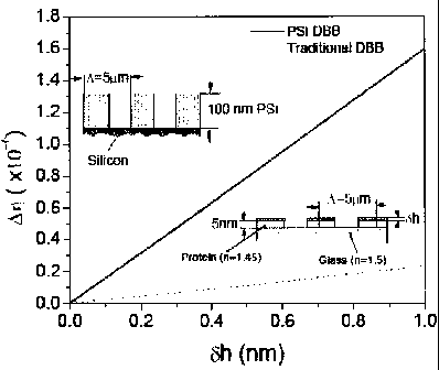
[0113] In Fig.24 the calculated diffraction efficiency variation for a
traditional DBB with a
protein grating (n=1.45) of height h=5nm and period = A5 tm on a glass
substrate (n=1.5), and
for a pSi-DBB with low-porosity (p=0.61) grating of thickness D=100nm on a
silicon substrate,
both as a function of 6h in the traditional DBB, where fanalyte = 6h/D in the
pSi-DBB, was plotted.
[00114] The calculations show an increase of the sensitivity of about 8 times,
without any
optimization of the pSi structure. In addition to the sensitivity enhancement,
which is essentially
CA 02706053 2010-05-31
Attorney Docket No. 093386-9018-USOO (VU10107)
due to the use of a higher original grating, there are other important
advantages in the use of pSi
for the realization of DBBs: (1) The surface available for protein binding in
the pSi-DBB sensor
is much larger than in the traditional DBB sensor, and so the promptness of
the detector may be
enhanced as well as its sensitivity; (2) It has been demonstrated that DBB
efficiency can be
improved exploiting effects of field localization near the grating. This could
be easily
implemented in a pSi device by realizing the grating on a pSi waveguide.
26