Note: Descriptions are shown in the official language in which they were submitted.
CA 02707551 2013-01-15
30673-15
CIRCUIT ARRANGEMENT FOR CONTROLLING LIGHT EMITTING DIODES
The invention relates to a circuit arrangement
for controlling light-emitting diodes
(LEDs), which are combined in groups including at least
one driver which has outputs for supplying electric current
to the LEDs and a control input for adjusting the electric
current supplied to the LEDs.
Such a circuit arrangement is well-known in the state of the
art and is used for example for controlling LED's of a bill-
board or indicator board. As a driver, by which for example
a group of sixteen LEDs is energized or, respectively, sup-
plied with electric current, a multitude of different types
is available. All have in common that the current supplied
to the LEDs is adjustable by means of a resistor which is
connected to the control input.
When the light output of an LED group, that is, the light
output of the LEDs or the LED group controlled by the driver
is to be changed, the resistance must be changed. To this
end, the resistor may be in the form of a potentiometer.
Since the light output of the LED groups _often needs to be
adjusted to the ambient of the LED group, a corresponding ad-
justment of the resistor is necessary. This however is quite
costly, if a multitude of LED groups is combined to an indi-
cator board.
1
=
=
CA 02707551 2013-01-15
30673-15
A big problem in the adjustment of the light output of a
LED group (or respectively, the output current of the respec-
tive driver unit), for example, of an indicator board resides
in the fact that one has to be within reach of the resistor
or respectively the driver and, consequently, the LED group
so that the light output change cannot be satisfactorily
monitored. When, for example, the light output of a LED
group is to be changed in order.to adjust the light output of
a new LED group to the light output of the adjacent LED
W groups as it is necessary for example upon the replacement of
a defective LED group by a new LED group, it is generally
necessary that, after a change of the resistor setting the
repair person moves away from the indicator board to be able
to better judge the brightness of the new LED group in rela-
tion to the brightness of the adjacent LED groups. If the
brightness is still not correct the repair person has to re-
turn to the indicator board to change the resistance value
and again has to move away from the indicator board for judg-
ment. This needs to be repeated until the brightness is cor-
rect. This procedure however is very unsatisfactory.
A further problem with the known control of LEDs resides in
the fact that Lhe brightness of the LEDs cannot be changed
continually during operation. It is, for example, not possi-
ble so far, to adjust the brightness of the LEDs during op-
eration to the ambient light conditions without problems.
The LEDs of an indicator board have for example the same
.brightness in daylight with the sun shining as they have at
night when the moon is shining.
It is the object of some embodiments of the present invention to provide a cir-
cuit arrangement for controlling light emitting diodes in
such a way that the brightness of an LED group is more easily
2
=
CA 02707551 2013-01-15
30673-15
adjustable and that it can also be changed during normal op-
eration in a simple way.
In accordance with an aspect of the present invention, a circuit arrange-
ment for the control of light emitting diodes (LEDs)which are
combined in groups including at least one driver which has
outputs for supplying current to the LEDs and a 2ontrol in-
put for adjusting the current being supplied to the LEDs, is
characterized in that the control input is connected to the
output of a voltage source.
As a result of Lhu control input of the driver being con-
nected to the output of a voltage source, the current sup-
plied to the LEDs and, consequently the brightness of the
LEDs supplied with current by the driver can be adjusted in
a simple manner. It is particularly advantageous if the volt-
age source is controllable.
For the adjusi,ment of the voltage of the voltage source, it
is not necessary to be in the proximity of the voltage source
since there is no need for manually adjusting a component in
order to adjust the voltage of the voltage source. The volt-
age of a voltage source can be adjusted in a simple manner by
changing electrical values such as the current or the volt-
age. It is therefore possible to control the voltage of the
voltage source in such a way that it assumes a value depend-
ent on the brightness of adjacent LEDs. In particular, the
voltage of a voltage source can he adjusted in a simple man-
ner by remote control, wherein the remote control may be con-
nected to the voltage source by wire or wirelessly. In this
3
CA 02707551 2013-01-15
30673-15
way, it is advantageously possible to directly visually moni-
tor the effects of a change of Lilo voltage applied by the
voltage source to the control input of the drive with respect
to the brightness of the LEDs. This substantially facili-
tates the adjustment of the brightness ot the LEDs to the
ambient. =
It is particularly advantageous that the control input of the
voltage source can be connected to an adjustable voltage di-
vider whose input voltage is adjustable. In this way, it is
possible to adjust the output voltage and, accordingly, the
brightness of the LEDs by means of the voltage divider first
with a predetermined overall voltage applied to the voltage
divider in such a way that the brightness of the LEDs corre-
sponds to a base value with which the indicating board is op-
erated. The voltage divider is herein so adjusted that the
base brightnesE corresponds to the base brightness of the ad-
jacent LEDs. As base brightness advantageously a value is
taken at which the LEDs 3 are energized by about half of the
maximum admissible current.
When the ambient light changes for example by sunlight the
overall voltage applied to the voltage divider may be in-
creased. As a result, also the voltage provided by the volt-
age divider and consequently the voltage supplied by the
voltage source and the current flowing through the LEDs as
well as the brightness or the .LEDs are increased. If sev-
eral boards are combined to an indicating table the bright-
ness of all LEDs can be changed by changing the overall
voltage applied to the respective voltage dividers. By
changing the total voltage furthermore the energy that is
- consumed by an indicating boards or table can be influenced
in a simple manner. It is therefore possible to operate the
4
CA 02707551 2013-01-15
30673-15
indicating boards or table with an intelligent energy manage-
ment.
Since it has been found that the control inputs of several
drivers can be connected to a common voltage source as this
is done in a particular embodiment, it is advantageously pos-
sible to combine several LED groups in a common board and to
connect the control inputs of the drivers of the LEDs ar-
ranged on the board to a common volLage source. In this way,
the brightness of a multitude of LED's can be jointly ad-
justed in a simple manner.
Then, however, it is no longer possible to change the bright-
ness of the LEDs combined on a board relative to one an-
other; but this presents generally no problem, since the
LED's generally are manufactured all in a particular produc-
tion run and therefore have all the same properties. That
is, the brightness of the LEDs combined in a board is essen-
tially the same.
However, if, after passage of an extended period, a board
needs to be replaced, the brightness of the LED's arranged on
the replacement board is generally different from the bright-
ness of the LEDs on the remaining adjacent boards because of
25- aging of the remaining LED's so that the brightness of the
LEDs on the replacement board needs to be adjusted. In order
to have a high-quality indication, the base brightness of the
LED groups should be adapted to one another. Since an indi-
cating board may often have more than thousand LED groups,
the expenditures for an adaptation of the base brightness of
the LED groups is correspondingly high. Dy means of the cir-
cuit arrangement according to the invention, an adaptation of
the brightness of a new board is easily possible, particu-
larly for an indicating board with a plurality of LEDs corn-
5
CA 02707551 2013-01-15
30673-15
bind in groups. In this connection, it is particularly
advantageous that the voltage source can be remotely
controlled.
In one aspect of the present invention, there is provided a
circuit arrangement for controlling light emitting diodes
(LEDs) combined in groups, said circuit arrangement comprising
a voltage source, at least one driver which includes outputs
via which current can be supplied to the LEDs, and a current
control input by means of which the current deliverable to the
LEDs is adjustable, the current control input being connected
to an output of the voltage source, the voltage source
including a voltage control input by means of which the output
voltage of the voltage source is controllable and the voltage
control input of the voltage source being connected to an
adjustable voltage divider whose total voltage is adjustable.
In another aspect of the present invention, there is provided
an LED indicating board comprising a plurality of groups of
combined LEDs, and a circuit arrangement for controlling the
groups of light emitting diodes (LEDs), said circuit
arrangement comprising a voltage source, at least one driver
which includes outputs via which current can be supplied to the
LEDs, and a current control input by means of which the current
deliverable to the LEDs is adjustable, the current control
input being connected to an output of the voltage source, and
the voltage source including a voltage control input by means
of which the output voltage of the voltage source is
controllable and the voltage control input of the voltage
source being connected to an adjustable voltage divider whose
total voltage is adjustable.
6
CA 02707551 2013-01-15
30673-15
Further particulars, Ceatures and advantages of the present
invention will become more readily apparent from the follow-
ing description of a particular embodiment with reference to
the accompanying drawings.
It is shown in:
Fig. 1 an embodiment of the circuit arrangement accord-
ing to the invention, and in
Fig. 2 a schematic representation of an indicating
board.
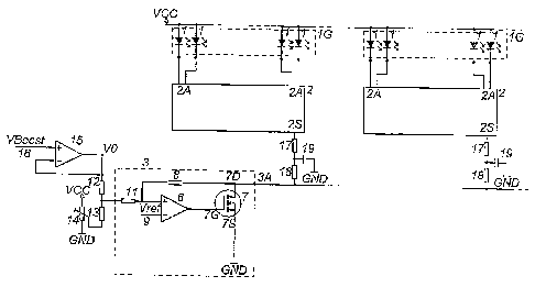
As shown in Fig. 1, in each case one group 10 of altogether
sixteen LEDs 1 is controlled by a driver 2 to the respective
outputs 2A of which the LED's 1 are connected. The respec-
tive driver 2, which may be for example a low voltage 16 Bit
Constant Current LED Sink Driver SDP16CP596 of the company ST
further includes a control input 28, which is connected to
the output 3A of a voltage source 3. Altogether, for exam-
ple, sixty LED groups 10 may be combined in a board and con-
trolled by a common voltage source 3. For the suppression
and for a basic adjustment of the current supplied by the
driver 2 to the LEDs 1, the control input 2S of the driver 2
is connected to the output 3A of the voltage source 3 via an
BC-network 17, 18, 19.
=
The voltage source 3 is of conventional design and includes a
first operational amplifier 6 whose output is connected to
the gate connection 7G of a field effect transistor 7 and,
consequently, controls the field effect transistor 7. The
drain connection 7D of the field effect transistor 7 which at
the same time forms the output 3A of the current source 3, is
6a
CA 02707551 2013-01-15
30673-15
connected, via a resistor 8, to the plus input of the Cirst
operational amplifier 6. The source connection 7S of the
field effect transistor 7 is connected to mass. At the nega-
tive input ot the first operational amplifier 6, a self-
generated reference voltage VI k is connected. The constant
reference voltage Vrtet and the values of the building compo-
nents (for example, resistance values) used in this circuit
part were so selected that, with a certain analog value of
the input voltage VB005t, the desired associated analogous
io voltage is obtained at the setting input 25 of the driver 2.
The first operational amplifier 6 operates in this connection
in combination with the field effect transistor 7 as an in-
verting amplifier,
The positive input of the first operational amplifier 6 is
connected via a resistor 11 to a voltage divider which com-
prises two resistors 12, 13 and a potentiometer 14. The
voltage divider is fed by a second operational amplifier 15,
whose plus input forms a boost input 16 of the voltage source
3. The negative input of the second operational amplifier 15
is connected to the output of the second operational ampli-
fier 15.
Depending on the voltage Vbõst at the boost input 16 the volt-
age applied by the voltage source 3 to the inputs 25 of the
driver can be adjusted. A basic voltage applied to the volt-
age source 3 at a first predetermined voltage Vsoont to the
boost input 16 to the control inputs 25 of the driver 2 can
be set by means of the potentiometer 14, That means that, by
.30 means of the potentiometer 14, the brightness present at the
first predetermined voltage Vboost of the LED's which are con-
trolled by the respective drivers 2 can be adapted to the
brightness of adjacent LEDs whose drivers are controlled by
another voltage source.
7
CA 02707551 2013-01-15
30673-15
The first predetermined voltage Vcõ,,, is so selected that the
LED's are operated by a current which corresponds about to
half the maximally admissible current. If the brightness of
the LEDs 1 is to be increased because for example the
brightness of the ambient light has been increased the volt-
age VbooRr. is increased correspondingly. In this way, the to-
tal voltage V present at the voltage divider is increased
whereby the voltage applied by the voltage source 3 to the
driver 2 is increased so that the drivers 2 connected to the
output 3A of the voltage source 3 all increase the current
flow through the controlled LEDs, which results in a uniform
brightness change of the respective LED's.
As apparent from Fig. 2, the indicator board 4 consists of a
plurality of boards 5, of which each comprises a plurality of
groups of sixteen LEDs. An indication table may for example
include six to sixty boards wherein a single board includes
sixty groups having each sixteen LEDs.
If, for example, the board 5' shown in Fig, 2 is to be re-
placed by a new board, the brightness of the LEDs disposed
on the board 5' is adapted by means of the potentiometer 14
at Lhe same predetermined voltage Vbõut to the brightness ot
the adjacent board 5".
8