Note: Descriptions are shown in the official language in which they were submitted.
CA 02708522 2010-06-08
WO 2009/091723 PCT/US2009/030831
LOW PROFILE BACKLIGHT APPARATUS
BACKGROUND
Brightness enhancement films (BEFs), otherwise known as prism sheets, are made
by
forming a prism pattern on optical substrate film. The BEFs serve to
concentrate light toward the
output side of a backlight, when they are incorporated onto the front surface
of that backlight. The
prism sheet is, in essence, a film for boosting brightness levels while
keeping the power consumed
a constant. FIG. 1 illustrates a common architecture employed in liquid
crystal displays 1 (LCDs).
A cold fluorescent light 5 and a light guideplate 6 act as a backlight to
transmit light through first
and second BEFs 4a and 4b, otherwise known as prism sheets, that are crossed
90 relative to each
other. Prior to entering the first BEF 4a the light passes through a first
diffuser 3a. Light
emanating from the second BEF 4b passes through a second diffuser 3b and
finally through an
LCD panel 2. In the configuration illustrated in FIG. 1, the BEFs 4a,b provide
an output radiation
(light) pattern that is restricted to about 210.
The BEFs 4a,b utilize a prismatic structure to provide brightness gain. The
BEFs 4a,b direct
the light through the LCD panel 2, thereby providing increased brightness
toward the on-axis
viewer. A single sheet (e.g., the first BEF 4a) provides up to 60% increase in
brightness and two
sheets crossed at 90 (e.g., the first and second BEFs 4a,b as shown in FIG.
1) can provide up to
120% brightness increase. The increased brightness provides power savings.
Single sheets of
BEFs 4a may be used with LCD panels 2 in monitors and televisions. Crossed
sheets of BEFs 4a,b
may be used with LCD panels 2 in notebook personal computers.
As shown in FIG. 1, a backlight is a form of illumination used in LCDs.
Backlights
illuminate the LCD from the side or back. Backlights increase visibility of
small and large displays
in low light or bright sunlight conditions. In computer displays and LCD
televisions, backlights
produce light in a manner similar to a CRT display. Backlights can be color or
monochrome.
Color LCD displays such as those used for television or computer monitors
generally use white
backlights to cover most of the color spectrum.
Large area backlight systems are used in a variety of large display systems
including laptop
or notebook computer systems, large screen LCD screens, sunlight readable
avionic/automotive
displays, air traffic control displays, and medical display systems, to
mention a few. Systems such
as commercial aircraft cockpit displays and automotive displays including
global positioning
systems (GPS) navigation systems require extremely bright backlit LCD
displays.
Twisted nematic (TN) and super-twisted (STN) LCD are types of displays that
suffer from
poor performance when viewed at wide viewing angles due to the optical
characteristics of TN and
CA 02708522 2010-06-08
WO 2009/091723 PCT/US2009/030831
STN liquid crystal materials. Color shift and decreased contrast are due to
differences in the optical
path length of light rays transmitted through the liquid crystal material
viewed at high viewing
angles versus light rays viewed at near-normal angles. LCD designers have
tried to overcome this
problem by careful choice of liquid crystal materials and by utilizing various
internal LCD
modifications.
Conventional large area backlight systems utilize an array of point sources of
radiant
electromagnetic energy such as light emitting diodes (LEDs) providing direct
light emission to an
output aperture surface of the backlight system. An optical cavity is formed
between the point
sources and the output aperture surface. Conventional backlight systems
require relatively deep
optical cavities in order to mix the light within the optical cavity.
Diffusers provide better surface
uniformity, but reduce the light output and decrease the overall efficiency of
the backlight system.
In addition, it is difficult to reduce or tailor the field of view with
conventional LED/waveguide
technology for backlight systems. There is a need for a new and improved
backlight system to
collimate the light output from the point sources and direct the collimated
light to an output
aperture and diffuser to spread the light output and tailor it to the output
field of view.
SUMMARY
In one embodiment, a backlight apparatus comprises a point source of radiant
electromagnetic energy. A totally internally reflection (TIR) lens having a
vertical central axis is
located along a path of the radiant electromagnetic energy to receive and
evenly distribute the
radiant electromagnetic energy at an output face. The radiant electromagnetic
energy exiting the
TIR lens is substantially collimated and defines vertical optical paths
parallel to the vertical central
axis. A first diffuser receives the radiant electromagnetic energy from the
output face of the TIR
lens and spreads the radiant electromagnetic energy to a predetermined first
angle relative to the
vertical optical paths.
FIGURES
FIG. 1 illustrates a common architecture employed in liquid crystal displays
(LCDs)
FIG. 2 illustrates one embodiment of a low profile backlight apparatus
comprising a lens
array.
FIG. 3 is a cross-sectional view of the lens array shown in FIG. 2 taken along
line 3-3.
FIG. 4 is a cross-sectional view of one embodiment of a lens element
comprising a lens
acting as a backlight illumination source for an LCD element.
FIG. 4A is a magnified view of a portion of the lens element shown in FIG. 4.
- 2 -
CA 02708522 2010-06-08
WO 2009/091723 PCT/US2009/030831
FIG. 5 is a cross-sectional view of one embodiment of a lens element
comprising a lens
acting as a backlight illumination source for an LCD element.
FIG. 6 is a cross-sectional view of one embodiment of a lens element
comprising a lens
acting as a backlight illumination source for an LCD element.
FIG.7 is a cross-sectional view of one embodiment of a lens element comprising
a lens
acting as a backlight illumination source for an LCD element.
FIG. 8 illustrates one embodiment of a low profile backlight apparatus
comprising a lens
array.
FIG. 9 is a cross-sectional view of the lens array shown in FIG. 8 taken along
line 9-9.
FIG. 10 illustrates one embodiment of an individual square lens element
inscribed within a
circle of radius R.
FIG. 11 illustrates one embodiment of an individual hexagonal lens element
inscribed
within a circle of radius R= S.
DESCRIPTION
Before explaining the various embodiments in detail, it should be noted that
the
embodiments are not limited in their application or use to the details of
construction and
arrangement of parts illustrated in the accompanying drawings and description.
The illustrative
embodiments may be implemented or incorporated in other embodiments,
variations and
modifications, and may be practiced or carried out in various techniques. The
backlight apparatus
configurations disclosed below are illustrative only and not meant to limit
the scope or application
thereof. Furthermore, unless otherwise indicated, the terms and expressions
employed herein have
been chosen for the purpose of describing the illustrative embodiments for the
convenience of the
reader and are not to limit the scope thereof.
In one embodiment, a backlight apparatus comprises an array of total internal
reflection
(TIR) optic elements to collimate light from a point source, pass the
collimated light through and
LCD element, and subsequently spread the light to a predetermined field-of-
view. The field-of-
view may be determined from the perspective of the viewer. The collimated
light may be
redirected to the predetermined field-of-view using a diffuser system. In one
embodiment, a
backlight apparatus comprises an LED point source and an array of TIR lenses
to collimate the
light from the LED point source. The collimated light may be redirected to a
predetermined field-
of-view using a holographic diffuser.
FIG. 2 illustrates one embodiment of a low profile backlight apparatus 8
comprising a lens
array 10. Those skilled in the art will appreciate that a low profile lens may
be defined as a lens
-3 -
CA 02708522 2010-06-08
WO 2009/091723 PCT/US2009/030831
having an f# (e.g., the ratio of the focal distance to the diameter of the
lens) in the range of
approximately 0.2 to 0.3 as a function of the index of refraction of the
material. For example,
polycarbonate as anf#:=10.2, optical grade acrylic has an f# ,==, 0.2,5 and
silicone has anf# 0.3.
The lens array 10 employs optic elements to collimate light emitted by a point
source, pass the
collimated light through an LCD element, and subsequently spread the light
transmitted through the
LCD element to a predetermined field-of-view. The field-of-view may be
determined from the
perspective of a viewer. In the illustrated embodiment, the lens array 10 is
formed as a 4 x 4 array
of individual square lens elements 12. The lens elements 12 may be referred to
as pixels. It should
be understood that the array may include any integer number of individual lens
elements 12
arranged as an n x m matrix, where n and m are any integer and in one
embodiment n = m. The
size and shape of the individual lens elements 12 may be selected depending on
the particular
application. In the illustrated embodiment, each lens element 12 defines a
square. In other
embodiments, the lens elements 12 may be formed of numerous sizes and shapes,
such as the
hexagonal shaped lens element 142 shown in FIG. 8, for example. In other
embodiments, the shape
of the lens elements 12 may be selected from numerous other suitable polygonal
shapes. Therefore,
the embodiments are not limited in this context.
FIG. 3 is a cross-sectional view of the lens array 10 taken along line 3-3.
Each of the
individual lens elements 12 comprises a lens 14 and a point source 16 of
radiant electromagnetic
energy. In one embodiment, each of the individual lens elements 12 may
comprise total internal
reflection (TIR) optic elements to collimate light from the point source 16
and a diffuser to
subsequently spread the light rays of the collimated light 42 to a
predetermined field-of-view from
the perspective of the viewer, for example. The point source 16 for the
backlight apparatus 8 may
comprise any source of radiant electromagnetic energy including, for example,
an incandescent
light bulb, one or more light-emitting diodes (LEDs), an electroluminescent
panel (ELP), one or
more cold cathode fluorescent lamp (CCFL), or hot cathode fluorescent lamps
(HCFL). The point
source 16 may generate color light although white light LED backlighting is
also contemplated in
the various embodiments of the backlight apparatus 8. In one embodiment, the
point source 16
may comprise one or more red-green-blue (RGB) LED point sources. The light
emitted by the
LEDs is slightly diffused by a diffuser 18. The diffuser 18 slightly increases
the angular spectrum
of the collimated light 40 to the pattern of the light 42 to minimize or
eliminate interstitial dark
lines 17 produced by the lens-to-lens juxtaposition of the lenses 14. The
angular spectrum of the
light 42 may be slightly increased to approximately 6 to 10 relative to
the collimated light 40.
The collimated light 40 is passed through the LCD element 22, and subsequently
the angular
spectrum of the light is further increased or spread to the pattern of the
light 44 by a diffuser 20,
- 4 -
CA 02708522 2015-12-18
and in particular, is diffused in the horizontal direction H. The light rays
of the collimated light 40
propagate along vertical optical paths parallel to a vertical central axis 24.
The light 40 is
substantially collimated such that the light propagates at an angle of less
than approximately +/-2
relative to the vertical optical paths for a TIR lens of 25.4mm, for exainple.
The light 40 emanating from the point source 16 is collimated in the vertical
direction V
by the lens 14. Collimating the light 40 in the vertical direction V minimizes
chromatic aberration
and removes chromatic dispersion due to different path lengths of the light
emitted by the RGB
point source 16. The collimated light 40 is redirected to a specified or
predetermined field-of-view
using a diffuser system. In one embodiment, the diffuser system may comprise
one or more
diffusers. In one embodiment, the collimated light 40 may be transmitted
through the diffuser 18
and subsequently through an LCD element 22. In one embodiment, the diffuser 18
may be a
microstructured surface formed on the flat surface of the exit face 38 (FIG.
4) of the lens 14 or
may be formed as a separate element. In the illustrated embodiment, the
diffuser 18 is formed as
separate element and is configured to collimate the light 42. The light 42
emanating from the LCD
element 22 is subsequently transmitted through a diffuser 20 that is
configured to spread the light
rays of light 44. The diffuser 20 spreads the light 44 to a predetermined
field-of-view, thus
providing a wide viewing angle for the viewer. The diffuser 20 may be
implemented as a
holographic diffuser, otherwise known as a kinoform diffuser, to redirect or
spread the collimated
light 40 to output light 44 at a predetermined field-of-view. Examples of
holographic diffusers are
described in "An Overview of LED Applications for General Illumination"
(Conference
Proceedings Paper), David G. Pelka, Kavita Patel, SPIE Vol. 5186, November
2003; and "Keen
Forms of Kinoforms - Kinoform -based Diffusers Help Lighting Designers
Leverage Unique LED
Advantages," David G. Pelka, OE Magazine, Vol. 3 No. 10, p. 19, October 2003.
In one embodiment, the backlight apparatus 8 illustrated in FIGS. 2 and 3 is
sufficient to
illuminate a substantially large area LCD as may be required in a specific
application (e.g., large
LCD televisions). The backlight apparatus 8 may be substantially wide in the
horizontal direction
H and substantially thin in the vertical direction V to eliminate the need for
brightness enhancing
films (e.g., see FIG. I and associated description above). The collimated
light 40 transmitted
through the diffuser 18 and a TN or STN LCD element 22 remains substantially
collimated to
maximize contrast and minimize color shift, but may be spread slightly from an
angle of
approximately +/-2 up to approximately +/-10 relative to the vertical
optical paths defined by the
collimated light 40. Because most modem applications demand wider viewing
angles, the diffuser
20 may be formed as a diffusing screen to further spread the collimated light
40, 42 after it has
- 5 -
CA 02708522 2015-12-18
passed through the diffuser 18 and the LCD element 22. The diffuser 20 further
spreads the light
44 to an angle greater than +/-10 relative to the vertical optical paths
defined by the collimated
light 40 after it has passed through the LCD element 22. The lens array 10
provides high optical
efficiency, low backscatter of ambient light to maintain high image contrast,
and wide viewing
angle.
It is desirable that the highly collimated light 40 may be generated by a
sufficiently thin
(e.g.,f 0.25 for an index of refraction that is > 1.5 for a
transparent material) backlight point
source 16 and optics to preserve the overall thinness (e.g., low profile) of
the backlight apparatus 8.
Thinner backlights are more desirable given the trend of producing larger and
thinner displays for
computers and televisions, for example. A substantially thin backlight
apparatus 8 maximizes
contrast and minimizes color shift with respect to the viewing angle of the
LCD element 22. Such a
solution is independent (external) of the LCD element 22 and can be made
without modifying the
LCD element 22 internally. This provides a substantially improved low profile
backlight apparatus
8 with reduced cost for use in many applications such as LCD monitors,
notebook computers, auto
navigation displays, avionics displays, air traffic control displays, and
medical display systems,
among others whether or not described herein. In one embodiment, the backlight
apparatus 8 may
be formed with a vertical thickness of approximately 10-13 inm. The individual
lens elements 12
may be formed as TIR lens elements having a vertical thickness of
approximately 7-9 mm. The
diffusers 18, 20 may be formed with a vertical thickness of approximately 3-4
min to provide a thin
and efficient optical diffuser stack.
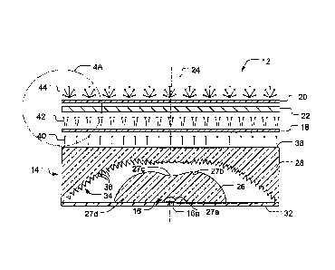
FIG. 4 is a cross-sectional view of one embodiment of the lens element 12
comprising the
lens 14 acting as the backlight illumination source for the LCD element 22. In
the illustrated
embodiment, the lens 14 has a vertical central axis 24. The lens 14 comprises
a source ray deviator
lens 26, e.g., acting on the light emitted by the point source 16, a TIR lens
28, and the point source
16 comprising an RGB LED 16a. TIR lens elements similar to the lens 14 and
source ray deviator
lens elements similar to the source ray deviator lens 26 are disclosed in U.
S. Patent No. 5,577,493.
It is desirable that the TIR lens 28 have numerous small facets 34, having
entry faces 36 and, in
the illustrated embodiment, an exit face 38 with a flat surface. In one
embodiment, the diffuser 18
may be a microstructure surface formed on the flat surface of the exit face 38
to blur any spatial
structure imposed by the facets 34. In the illustrated embodiment, the
diffuser 18 is formed as a
separate element from the TIR lens 28 and is vertically spatially located from
the exit face 38 to
integrate any blurring caused by the facets 34 such that they are not visible
to the viewers of the
LCD element 22. The deviator lens 26 also provides thermal protection for the
TIR lens 28 when
the point source 16 is a high-power output point
- 6 -
CA 02708522 2015-12-18
source. The TIR lens 28 may consist of a plastic and a smooth source ray
deviator lens 26 can be
made of high temperature plastic, silicone, or glass, which can withstand high
temperatures and act
as an insulating barrier between the TIR lens 28 and the point source 16. The
base of the lens 14
may be formed on a substrate 32 to provide greater angular spectrum.
The deviator lens 26 may be used in conjunction with a reflector similar to
the reflector 104
shown in FIG. 6) and the TIR lens 28. In one embodiment, the deviator lens 26
has a inushrooin
profile. In the illustrated embodiment, the deviator lens 26 has a
hemispherically concave inner
surface 27a of greater curvature (i.e., smaller radius) than the varying
curvatures of a convex outer
surface 27b, such curvatures decreasing at regions toward the axis 24,
becoming concave
(detnagnifying) at a central outer surface 27c. A flat bottom surface 27d is
coplanar with the
outerinost tip of TIR lens 28. It is thus situated so as to interfere with
neither the TIR lens 28 nor a
reflector, if used. The deviator lens 26 is positioned along the path of the
light from the point
source 16 and is positioned between the point source 16 and the TIR lens 28.
The deviator lens 26
deviates light towards portions of the TIR lens 28 spaced from the vertical
axis 24 to more evenly
distribute the light 40 flux at the output of the TIR lens 28. The deviator
lens 26 is a non-imaging
optical element to transform the cumulative angular distribution of intensity
of light from the point
source 16 into a different distribution. The TIR lens 28 forms a uniform
distribution of the light 40
exiting the flat surface of the exit face 38 of the TIR lens 28. Additional
examples of TIR lens
elements similar to the lens 14 are disclosed in U. S. Patent Nos. 5,404,869
and 5,655,832.
FIG. 4A is a magnified view of a portion of the lens element 12 shown in FIG.
4. As
shown in FIG. 4A, collimation of the light 40 exiting the flat surface exit
face 38 of the TIR lens 28
is maintained by the diffuser 18. Light 42 exiting the diffuser 18 remains
substantially collimated,
but may be spread slightly to an angle of approximately 6 , and in some
embodiments up to
approximately 100, relative to the vertical optical paths defined by the
collimated light 40 before
passing through the LCD element 22 to maximize contrast and minimize color
shift. As previously
discussed, the collimated light 42 is transmitted through the LCD element 22
and is subsequently
transmitted through the diffuser 20. The diffuser 20 spreads the light 44 more
than 20 to provide
a wider field-of-view in the horizontal direction H and some embodiments tnore
than 30 in the
horizontal direction H.
FIG. 5 is a cross-sectional view of one embodiment of the lens element 12
comprising a
lens 90 acting as the backlight illumination source for the LCD element 22. In
the illustrated
embodiment, the lens 90 has a vertical central axis 24. The lens 90 comprises
the TIR lens 28, the
diffuser optic 54, and the point source 16 comprising the LED 16a previously
described. The
- 7 -
CA 02708522 2010-06-08
WO 2009/091723 PCT/US2009/030831
diffuser optic 54 is partially embedded within a suitable hole, channel, or
recess 92 that extends
into a substrate 94. Light emanating from the point source 16 is diffused by
the diffuser optic 54
and is transmitted by the numerous entry faces 36 of the small facets 34
through the exit face 38 of
the TIR lens 28. The angular spectrum of the light 40 is slightly increased in
the horizontal
direction H by the diffuser 18. The light 42 emanating from the diffuser 18 is
substantially
collimated to an angle of approximately 6 , and in some embodiments, up to
approximately 10 ,
relative to the vertical optical paths defined by the collimated light 40
before passing through the
LCD element 22. As previously discussed, the collimated light 42 is
transmitted through the LCD
element 22 and is subsequently transmitted through the diffuser 20. The light
44 emanating from
the diffuser 20 is spread more than 10 by the diffuser 20 to provide a wider
field-of-view.
FIG. 6 is a cross-sectional view of one embodiment of the lens element 12
comprising a
lens 100 acting as the backlight illumination source for the LCD element 22.
In the illustrated
embodiment, the lens 100 has a vertical central axis 24. The lens 100
comprises the TIR lens 28,
the point source 16 comprising the LEDs 16a, b, as previously described, and a
reflector 104 and a
diffuser optic 102 located above the reflector 104. The reflector 104 is to
reflect light from the
point source 16 back towards the diffuser optic 102 and into the TIR lens 28.
The reflector 104
may be formed as an integrating hemisphere comprising a highly reflective
surface and may be
referred to generally as a mixing chamber. The reflector 104 is located below
a substrate 106. The
LEDs 16a, b are located within the reflector 104 below the substrate 106.
Light emitted by the
LEDs 16a, b is reflected by the interior reflecting surface of the reflector
104 and are diffused by
the diffuser optic 102 and are transmitted by the numerous entry faces 36 of
the small facets 34
through the exit face 38 of the TIR lens 28. The light 40 is collimated by the
diffuser 18. The light
42 emanating from the diffuser 18 is substantially collimated to an angle of
approximately 6 , and
in some embodiments up to approximately 10 , relative to the vertical optical
paths defined by the
collimated light 40 before passing through the LCD element 22. As previously
discussed, the
collimated light 42 is transmitted through the LCD element 22 and is
subsequently transmitted
through the diffuser 20. The light 44 emanating from the diffuser 20 is spread
more than 100 by
the diffuser 20 to provide a wider field-of-view.
FIG. 7 is a cross-sectional view of one embodiment of the lens element 12
comprising a
lens 120 acting as the backlight illumination source for the LCD element 22.
The lens 120
comprises the deviator lens 26 and the TIR lens 28 previously described. The
lens 120 is located
above a white diffuser 122 formed with apertures 124. The point sources 16 are
located on either
side of the apertures 124. A solid white diffuser 126 is spatially located in
the vertical direction
from the white diffuser 122 to define a highly diffusely reflecting
integrating cavity 130 to mix
- 8 -
CA 02708522 2010-06-08
WO 2009/091723 PCT/US2009/030831
light 128 radiated from the point sources 16. Light 132 reflected by the solid
white diffuser 126 is
received through the apertures 124 and is presented to the deviator lens 26
and subsequently to the
TIR lens 28. The point sources 16 may comprise both white as well as RGB LED
sources of
radiation. In one embodiment, the reflecting integrating cavity 130 has a
reflectance exceeding
95%. The angular spectrum of the light 40 exiting the flat exit face 38 is
slightly increased by the
diffuser 18. Light 42 emanating from the diffuser 18 is substantially
collimated to an angle of
approximately 6 , and in some embodiments up to approximately 100, relative
to the vertical
optical paths defined by light 40 before passing through the LCD element 22.
As previously
discussed, the collimated light 42 is transmitted through the LCD element 22
and is subsequently
transmitted through the diffuser 20. The light 44 emanating from the diffuser
20 is spread more
than 100 by the diffuser 20 to provide a wider field-of-view.
The individual lens elements 12 described above may be formed in multiple
geometric
shapes depending on the desired optical efficiency. Thus, the lens elements 12
may be square,
rectangular, triangular, hexagonal and various other polygonal shapes. The
individual lens
elements 12 may be formed of any suitable polygonal shape or combinations
thereof that leave no
gaps in the areas where the light emanating from the LED is uncollimated. A
hexagonal lens
element is described below for illustrative purposes. The embodiments,
however, are not limited in
this context.
FIG. 8 illustrates one embodiment of a low profile backlight apparatus 140
comprising a
lens array 142. The lens array 142 employs optic elements to collimate light
emitted by a point
source, pass the collimated light through an LCD element, and subsequently
spread the light that
passes through the LCD element into a preferred field-of-view to provide a
wider viewing angle to
the viewer. In the illustrated embodiment, the lens array 142 is formed as an
array of individual
hexagonal lens elements 144. The lens elements 144 may be referred to as
pixels. It should be
understood that the array may include any integer number of individual lens
elements 144 arranged
as an n x m matrix, where n is any integer value and m is any integer value
and in one embodiment
n = m. The size and shape of the individual lens elements 144 may be selected
depending on the
particular application. In the illustrated embodiment, each lens element 144
defines a hexagon.
FIG. 9 is a cross-sectional view of the lens array 142 taken along line 9-9.
Each of the
individual lens elements 144 comprises a lens 146 and the point source 16 of
radiant
electromagnetic energy. In one embodiment, the lens elements 144 may comprise
TIR optic
elements to collimate light from the point source 16 and diffusers to
subsequently spread the
collimated light 42 to a predetermined field-of-view. The point source 16 for
the backlight
apparatus 140 may comprise any source of radiant electromagnetic energy. In
one embodiment the
- 9 -
CA 02708522 2010-06-08
WO 2009/091723 PCT/US2009/030831
point source 16 may comprise white LEDs and in another embodiment the point
source 16 may
comprise RGB LEDs.
FIG. 10 illustrates one embodiment of an individual square lens element 12
inscribed
within a circle 152 of radius R. The radius R of the circle 152 may be derived
based on the sides S
of the square lens element 12. The relative optical efficiency ELR of the
square lens element 12 may
be determined by the ratio of the respective area AL of the square lens
element 12 and the area Ac of
the circle 152. The area Ac of the circle 152 is given by:
Ac = n-R2
The area AL of the square lens element 12 is give by:
AL = S2
The relative optical efficiency ELR of the square lens element 12 is given by:
A S2
E ¨ =
LR Ac 71.R2
R= ______________
215
For S = 5.08cm (2in), R= 5.08/1.414 = 3.59cm. Accordingly,
Ac = 40.49cm2
AL = 25.81cm2
ELR A 25.81
= ______________________ = 0.64 = 64%
Ac 40.49
It is well known in the art that a well made injection molded circular TIR
lens has an optical
efficiency of approximately 0.85 or 85%. Therefore, the efficiency EL of the
square TIR lens
element 12 is approximately:
EL = 0.85* 0.64 = 0.544 = 54.4%.
FIG. 11 illustrates one embodiment of an individual hexagonal lens element 144
inscribed
within a circle 154 of radius R= S. The relative optical efficiency ELIR of
the hexagonal lens
element 144 may be determined by the ratio of the respective area AL/ of the
hexagonal lens
element 144 and the area Aci of the circle 154. Each of the six sides S of the
hexagonal lens
element 144 defines an equilateral triangle T.
The area AT of one of the triangles T is given by:
AT = ¨12SH
The area AL/ of the hexagonal lens element 144 is:
- 10 -
CA 02708522 2010-06-08
WO 2009/091723 PCT/US2009/030831
AL1 = 6AT =3SH
R= S
,
n
2
3-13-
AL I =64 = ¨2S2
The area Aci of the circle 154 is:
Ac, = 71-R2
The relative optical efficiency ELM? of the hexagonal lens element 144 is:
E-
ALI N5
= =3-
L112
AC1 gR2 276
For S = R = 5.08cm (2in):
Ac, = 81.07cm2
AL, = 67.05cm2
_ AL, 67.05
4.1
81.07
As previously stated, it is well known in the art that a well made injection
molded circular
TIR lens has an optical efficiency of 0.85 or 85%. Therefore, the efficiency
EL/ of the hexagonal
TIR lens element 12 is approximately:
ELI= 0.85*0.83 = 0.706 = 70.6%.
Although the a low profile backlight apparatus was illustrated and described
herein as
embodied in one or more specific examples, it is nevertheless not intended to
be limited to the
details shown. Various modifications and structural changes may be made
therein without
departing from the scope of the low profile backlight apparatus. Any
modifications and structural
changes are within the scope and range of equivalents of the claims.
Accordingly, it is appropriate
that the appended claims be construed broadly and in a manner consistent with
the scope of the low
profile backlight apparatus as set forth in the following claims.
- 11 -