Note: Descriptions are shown in the official language in which they were submitted.
CA 02708616 2010-06-09
1
Rear-Contact Solar Cell Having Extensive Rear Side Emitter Regions And Method
For
Producing The Same
FIELD OF THE INVENTION
The present invention relates to a rear-contact solar cell having extensive
rear side emitter
regions and also to a method for producing a rear-contact solar cell of this
type.
BACKGROUND TO THE INVENTION
Conventional solar cells have a front side contact, that is to say a contact
arranged on a
surface of the solar cell that faces the light, and a rear side contact on a
surface of the solar
cell that is turned away from the light. In these conventional solar cells,
the largest volume
fraction of a semiconductor substrate absorbing the light is of precisely the
semiconductor
type (for example p type) which is contacted by the rear side contact. This
volume fraction is
conventionally referred to as the base and the rear side contacts are
therefore conventionally
referred to as base contacts. A thin layer of the opposite semiconductor type
(for example n
type) is located in the region of the surface of the front side of the
semiconductor substrate.
This layer is conventionally referred to as the emitter and the contacts
contacting it are
referred to as emitter contacts.
In conventional solar cells of this type, the pn junction, which is crucial
for the collection of
current, is thus positioned just under the front side surface of the solar
cell. This position of
the pn junction is advantageous for an efficient collection of current in
particular on use of
semiconductor material of poor to moderate quality, as the highest generation
rate of charge
carrier pairs is present on the side of the solar cell that faces the light
and most light-
generated (minority) charge carriers thus have to cover only a short distance
to the pn
junction.
However, the emitter contacts arranged on the front side of the solar cell
lead, on account of
the partial shading associated therewith of the front side, to a loss in
efficiency. In order to
increase the efficiency of the solar cell, it is basically advantageous to
arrange both the base
contacts and the emitter contacts on the rear side of the solar cell. For this
purpose,
corresponding emitter regions have to be formed on the rear side of the solar
cell. A solar cell
in which both emitter regions and base regions are located on the side which
is turned away
from the light during use and in which both the emitter contacts and the base
contacts are
formed on the rear side is referred to as a rear-contact solar cell.
CA 02708616 2010-06-09
2
Rear-contact solar cells of this type, the current-collecting pn junction of
which is arranged at
least partly on the rear side of the solar cell, have to deal with the problem
that both the
emitter regions and the base regions are arranged next to one another on the
rear side of the
solar cell. Thus, the pn junction can no longer be formed along the entire
surface of the solar
cell; instead, the rear side emitter regions forming the pn junction together
with the volume
base region can now be formed only on a part of the rear side surface of the
solar cell. Rear
side base regions have to be provided therebetween for contacting the base.
As the diffusion length of the minority charge carriers to be collected by the
pn junction is
limited even in high-quality silicon, the area regions of the base regions
provided on the rear
side surface, which base regions substantially do not contribute to the
formation of the charge
carrier-collecting pn junction, should be as small as possible, in particular
in solar cells whose
current-collecting pn junction is arranged exclusively on the rear side of the
solar cell, in
order to adversely influence the effectiveness of the collection of current by
the pn junction
as little as possible. In this situation, the procedure is conventionally such
that the largest area
fraction of the rear side of the solar cell is provided with an emitter and
only narrow base
regions extend therebetween.
An example of a conventional rear-contact solar cell is illustrated
schematically in cross
section in Fig. 5. A semiconductor substrate 101 forms in its volume a base
region for
example of the p semiconductor type. Emitter regions 105 are formed on a rear
side surface
103. The emitter regions 105 cover the majority of the rear side surface 103.
Narrow, line-
shaped regions, at which base regions 107 of the semiconductor substrate 101
reach up to the
rear side surface 103, are left free between the elongate, finger-shaped
emitter regions 105 -
to which the cross section of the solar cell as shown in the drawing runs
perpendicularly. In
the region of the rear side surface, these base regions can be more heavily
doped than the
bulk volume of the base of the solar cell. The entire rear side surface 103 is
covered with a
dielectric passivating layer 109 which can have a low index of refraction, so
that it can serve
for example as a rear side reflector for the solar cell, and which can for
example be formed
from silicon dioxide. The passivating layer 109 has local openings 111 through
which emitter
contacts 113 can contact the emitter regions 105. Furthermore, the dielectric
layer 109 has
openings 115 through which base contacts 117 can contact the base regions 107
which reach
locally up to the rear side surface. The emitter contacts 113 and the base
contacts 117 are
separated from one another by narrow gaps 119 and thus electrically insulated.
CA 02708616 2010-06-09
3
In this type of solar cell, the base contacts 117 are slightly narrower than
the base regions 107
on the rear side surface 103. This ensures that the base contact 117 cannot
generate an
undesired short circuit with the emitter regions 105 even when the dielectric
layer 109 is not
perfectly electrically insulated, as the base contacts do not overlap with the
emitter regions
105 in projection.
In order to minimise production costs, in conventional rear-contact solar
cells such as are
illustrated in Fig. 5, the emitter contacts 113 and the base contacts 117 are
generally applied
in a common method step, for example by vapour depositing or sputtering-on of
metal, if
appropriate with subsequent electroplating, and are thus of substantially
uniform thickness.
However, the base contacts 117 are much narrower than the emitter contacts
113. However,
as both contacts 113, 117 have to discharge the same current, it is the case
that the emitter
contacts are much thicker than required when applying a metal layer thickness
for the
contacts that is sufficient for an efficient dissipation of current from the
base through the base
contacts. In other words, an unnecessarily large amount of material is
deposited on the more
extensive emitter contacts when base and emitter contacts are deposited in a
common process
step. However, the application of the metal coating for the contacts and also
the associated
material costs are a considerable portion of the total costs of the solar
cells.
It may therefore be desirable to form the metal contacts for both the emitter
and the base
contacts in roughly the same width and in this case to preferably make the
metal contacts as
wide as possible, so that an electrical resistance of the metal contacts that
is as low as
possible can be achieved at a low metal layer thickness.
In the alternative embodiment illustrated in Fig. 6 of a conventional rear-
contact solar cell,
the area fractions covered by the emitter contact 213 and by the base contact
217 respectively
on the rear side surface of the semiconductor substrate 201 are substantially
the same. As
however, in this rear contact solar cell too, regions of the rear side surface
that are as wide as
possible are to be covered with emitter regions 205, the base regions 207
extending between
the emitter regions 205 up to the rear side surface are narrower than the base
contacts 217
contacting these regions. In other words, the base contacts 217 reach
laterally into regions
where they overlap the emitter regions 205. In order to avoid short circuits
in the process, the
dielectric layer 209 has to be as effective an electrical insulator as
possible. However, the
formation of a very effectively electrically insulating dielectric layer 209,
which is in
particular compatible with the steps for producing the solar cell and the
loads placed on the
CA 02708616 2010-06-09
4
solar cell in the module, has proven to be a considerable technological
problem, in particular
in view of the fact that local short circuits may be tolerated at no point on
the area of the solar
cell which, in currently industrially manufactured solar cells, typically
comprises about 150
2
cm .
Furthermore, it has been observed that the emitter regions adjoining the rear
side surface of
the solar cell can be passivated only insufficiently by conventional processes
such as thermal
oxidation, in particular if the emitter regions are p-type emitters.
SUMMARY OF THE INVENTION
There may therefore be a need for a rear-contact solar cell and for a method
for producing a
rear-contact solar cell in which the above-mentioned drawbacks of conventional
rear-contact
solar cells can be at least partly avoided. In particular, there may be a
demand for a rear-
contact solar cell which, on the one hand, displays good current-collecting
properties on
account of a rear side emitter which is as extensive as possible and in which,
on the other
hand, the rear side metal contacts can be applied in a beneficial manner and
preferably at the
same time the risk of local short circuits caused by the metal contacts can be
minimised or
surface passivation on the rear side of the solar cell can be improved.
This need may be met by the subject matter of the independent claims.
Advantageous
embodiments of the present invention are described in the dependent claims.
A first aspect of the present invention describes a rear-contact solar cell
having a
semiconductor substrate, emitter regions along a rear side surface of the
semiconductor
substrate, base regions along the rear side surface of the semiconductor
substrate, emitter
contacts for electrically contacting the emitter regions and base contacts for
electrically
contacting at least some of the base regions. The semiconductor substrate has
a base
semiconductor type which may be either an n semiconductor type or a p
semiconductor type.
The base regions likewise have the base semiconductor type. The emitter
regions have an
emitter semiconductor type opposite to the base semiconductor type. The
emitter and base
regions formed on the rear side surface overlap at least in overlap regions,
the emitter regions
in the overlap regions reaching from the rear side surface deeper into the
semiconductor
substrate than the base regions.
This first aspect of the present invention may be regarded as being based on
the following
idea: Both emitter and base regions, which can both be electrically contacted
by
CA 02708616 2010-06-09
corresponding contacts on the rear side surface, are formed on the rear side
surface of the
semiconductor substrate. The fact that the emitter regions and the base
regions laterally
overlap in overlap regions and the emitter regions can run deeper there in the
interior of the
semiconductor substrate, whereas the base regions extend on the rear side
surface of the
semiconductor substrate, allows aims to be pursued that appear to be mutually
contradictory
in conventional rear-contact solar cells.
On the one hand, the base regions contacted by the base contacts can be formed
so as to be
comparatively wide or extensive on the rear side surface. In particular, the
base regions can
take up roughly the same area of the rear side surface as or a slightly larger
area of the rear
side surface than the base contacts, so that it is not absolutely crucial to
electrically insulate
the base contacts against the substrate surface by a dielectric layer arranged
thereunder. In
principle, the entire base region can be directly connected on its rear side
surface to the
corresponding base contacts without undesired short circuits occurring.
On the other hand, the area fraction of the base regions on the rear side
surface of the
semiconductor substrate, and thus also the area fraction of the base contacts,
may be roughly
the same size as the area fraction of the emitter partial regions or the
emitter contacts
adjoining the rear side surface. Thus, both the emitter contacts and the base
contacts can each
be formed at the same thickness necessary to avoid substantial series
resistance losses in the
contacts.
In the described rear-contact solar cell, a very large fraction of the rear
side surface can in this
case be covered with emitters on account of the emitter regions partly
overlapping the base
regions, so that the charge carrier-collecting properties can be very good on
account of the
extensive pn junction.
According to an exemplary embodiment which will be described hereinafter in
greater detail,
the emitter regions and the base regions can be formed by means of two
successive diffusions
of doping materials into the semiconductor substrate for producing a rear-
contact solar cell
according to the invention and in particular the overlap regions formed
therein. In this case,
the emitter regions can firstly be diffused in a first diffusion step, either
small partial regions,
in which the base regions on the rear side surface that are to be subsequently
produced are to
be in electrical contact with the base regions located further in the interior
of the
semiconductor substrate, being locally protected from the emitter diffusion or
the emitter
regions subsequently being locally opened/removed at these locations. In a
second diffusion
CA 02708616 2010-06-09
6
step, the base regions can then be formed on the rear side surface of the
semiconductor
substrate.
In this case, use may be made of what is known as the "emitter push effect" in
which, in two
successive process steps for diffusing doping materials into silicon for
example, the second
diffusion, albeit of the same or greater intensity, does not necessarily
compensate or
overcompensate for the first diffusion, as the second diffusion can push some
of the doping
materials of the first diffusion ahead of itself. In other words, the emitter
push effect may
cause the doping materials introduced during the first diffusion for producing
the emitter
regions to diffuse further into the interior of the semiconductor substrate,
whereas the doping
materials for producing the base regions diffuse-in from the surface of the
semiconductor
substrate. This can provide a structure in which the emitter regions and the
base regions have
roughly the same concentrations of dopants, but the emitter regions are
arranged further in
the interior of the semiconductor substrate than the base regions arranged on
the surface, so
that the desired overlap can occur. Experience has shown that the emitter push
effect is very
pronounced in particular when the second diffusion layer is a phosphorus
diffusion.
Alternatively, the overlapping structure may be achieved in that firstly a
deep emitter is
formed and subsequently shallower base regions are produced in the region of
base contacts
to be subsequently produced, the base regions being produced in such a way
that the emitter
doping which was beforehand originally contained in these regions is locally
overcompensated. Because the initially produced the emitter was formed deeper
than the
subsequently overcompensated base regions, the desired overlap of the two
regions may
again occur.
Doping materials can be introduced into the semiconductor substrate into the
desired regions
and depths also by other methods, such as for example ion implantation,
instead of diffusion
processes. As a further alternative, the structures according to the invention
can also be
produced by applying and structuring (or by applying in a structured manner)
semiconductor
layers by means of coating methods, for example epitaxy, heteroepitaxy or
other coating
methods.
Further features, details and possible advantages of embodiments of the rear-
contact solar cell
according to the invention will be described hereinafter.
CA 02708616 2010-06-09
7
The semiconductor substrate used for the rear-contact solar cell may for
example be a
monocrystalline or multicrystalline silicon wafer. Alternatively, thin layers
made of
amorphous or crystalline silicon or of other semiconducting materials can be
used as the
substrate.
Some of the emitter regions can extend along the rear side surface of the
semiconductor
substrate directly on the surface; however, parts of the emitter regions, in
particular in the
overlap regions, can also not directly adjoin the surface, but extend somewhat
deeper in the
interior of the semiconductor substrate. These internally "buried" emitter
regions can be in
electrical contact with the regions of the emitter regions that adjoin the
rear side surface, so
that they can also be electrically contacted from there by the emitter
contacts.
The emitter regions can be produced by diffusing dopants into the
semiconductor substrate.
For example, an n-type emitter region can be produced in a p-type
semiconductor substrate
by local diffusion of phosphorus. However, alternatively, the emitter regions
can also be
produced by other methods such as for example by ion implantation or alloying,
thus
producing what is known as a homojunction, that is to say a pn junction with
oppositely
doped regions of the same semiconductor basic material, for example silicon.
Alternatively,
the emitter regions can also be deposited epitaxially, for example be vapour
deposited or
sputtered-on, thus producing, depending on the selection of the applied
material,
homojunctions or what are known as heterojunctions, that is to say pn
junctions between a
base semiconductor-type first semiconductor material and an emitter
semiconductor-type
second semiconductor material, which are referred to as heterojunctions when
the base and
emitter semiconductors differ by more than just the conduction type (doping
type). A possible
example are emitter regions made of amorphous silicon (a-Si) which is vapour
deposited or
applied by means of PECVD on a semiconductor substrate made of crystalline
silicon (c-Si).
The base regions can also be produced by means of one of the above-mentioned
production
methods, although production by local diffusing-in of a dopant to form the
base regions may
be preferred.
The emitter regions and the base regions can each have, viewed from above onto
the rear side
surface of the semiconductor substrate, a comb-like structure in which in each
case linear,
finger-like emitter regions adjoin adjacent linear, finger-like base regions.
A nested structure
of this type is also said to be "interdigitated".
CA 02708616 2010-06-09
8
Both the emitter contacts and the base contacts can each be formed in the form
of a local
metal coating, for example in the form of finger-like grids. For this purpose,
metals, such as
for example silver or aluminium, can be deposited onto the base or emitter
regions locally,
for example through a mask or using photolithography, for example by vapour
deposition or
sputtering-on, or the metal contacts can be applied in the desired structure
by a printing
method such as screen printing or a dispensing method. In order to avoid short
circuits
between the emitter contacts and the base contacts, a respective electrically
insulating gap can
be provided between the two. This result can also be achieved by a metal layer
which is
applied over the entire surface and afterwards locally removed along the line
of the desired
contact separation.
An essential feature for the rear-contact solar cell according to the
invention are the overlap
regions in which both a base region and an emitter region are located on the
rear side of the
semiconductor substrate in the projection onto the rear side surface. In this
case, the base
region directly adjoins the rear side surface, whereas the emitter region is
displaced in this
region further into the interior of the semiconductor substrate, so that the
emitter in this
region can also be referred to as a "buried emitter". Both regions can in this
case extend very
close to the rear side surface of the semiconductor substrate, in particular
in view of the
thickness of the semiconductor substrate, which is conventionally high
compared to the
thickness of the emitter or base regions of for example a few micrometres and
can form about
200 m in a silicon wafer, for example. However, the emitter region can extend
deeper into
the semiconductor substrate than the base regions, in particular in the
overlap regions. For
example, the emitter region can extend down to a depth of more than 1 m,
preferably more
than 2 gm below the rear side surface, whereas the base regions reach into the
semiconductor
substrate for example to a depth of merely less than 1 m, for example a depth
of about 0.5
m.
In the fully processed solar cell, the emitter regions do not extend along the
entire rear side
surface of the semiconductor substrate; instead, there remain therebetween
small local
regions which do not have the emitter semiconductor type and which later serve
to produce
an electrical connection between the base regions formed on the rear side
surface and the
base regions in the interior of the semiconductor substrate. These connecting
regions, either
in which no corresponding emitter doping was caused as early as during the
production of the
emitter regions or in which previously produced emitter doping was
subsequently removed,
for example by etching-away or by laser ablation, or by local overcompensation
of the
CA 02708616 2010-06-09
9
emitter doping by base doping, may be line-like, for example parallel to the
base contacts to
be formed later, or dot-shaped.
According to one embodiment of the present invention, the emitter regions
extend along more
than 60 %, preferably more than 70 %, even more preferably more than 80 % and
more
preferably still more than 90 % of the rear side surface of the semiconductor
substrate and the
base regions extend along more than 25 %, preferably more than 40 % and more
preferably
between 45 % and 55 % of the rear side surface of the semiconductor substrate.
As a result of the fact that the emitter regions and the base regions partly
overlap, the total
area of the emitter regions facing the main volume and the base regions facing
the rear side of
the cell can add up to more than 100 % of the rear side surface of the
semiconductor
substrate. The further the emitter and base regions overlap in this case, the
greater the area
fraction of the emitter regions and the base regions may at the same time be.
The greater the
area fraction of the emitter regions is in this case, the more efficiently the
minority charge
carriers, which are produced in the interior of the semiconductor substrate by
incident light,
can be collected by the pn junction produced at the junction between the
emitter region and
the base region in the interior of the semiconductor substrate; this
contributes to a high
current density of the rear-contact solar cell. On the other hand, the greater
the area fraction
of the base regions facing the rear side of the cell is, the more extensive
the base contacts
covering these base regions may also be without producing short circuits to
the emitter
regions even if there is no electrically effectively insulating layer on the
rear side of the solar
cell. In elongate, finger-like contacts, this means that the base contacts may
be
correspondingly wide without there being a risk of overlap with laterally
adjacent emitter
regions. On account of the high width of the base contacts, series resistance
losses in the
metal contacts can be minimised even at relatively low metal layer
thicknesses.
According to a further embodiment of the present invention, an area of the
rear side surface
of the semiconductor substrate that is covered by the base contacts can be
between 70 % and
100 % of the area of the base regions on the rear side surface of the
semiconductor substrate.
In other words, 70 % to 100 %, preferably 90 % to 98 %, of the area of the
base regions can
be covered by base contacts. Low series resistances can be implemented in
these contacts on
account of the large area of the base contacts that is possible as a result.
On the other hand,
the base contacts preferably do not protrude laterally beyond the base regions
positioned
CA 02708616 2010-06-09
thereunder in order to avoid any short circuits between the base contacts and
the emitter
regions located next to the base regions.
According to a further embodiment of the present invention, a doping
concentration is higher
in the base regions on the rear side surface of the semiconductor substrate
than in base
regions in the interior of the semiconductor substrate. This can result from
the fact that the
base regions on the rear side surface are subsequently introduced, for example
are diffused,
into the semiconductor substrate during production of the solar cell. Heavily
doped
superficial base regions of this type can act as BSFs (back surface fields).
For example, the
doping concentration in the interior of the semiconductor substrate may be in
the range of
from 1 x 10¹⁴ CM -3 to 1 x 1017 cm-3, whereas the doping concentration in the
base regions on
the rear side surface may be greater than 1 x 1018 cm 3, preferably greater
than 1 x 1019 cm 3.
In addition to the BSF properties of such heavily doped base regions,
comparatively
extensive pn junctions between heavily doped emitter and base regions can be
produced in
the overlap regions. As described in greater detail in a patent application in
the name of the
applicant filed at the same time as the present application, planar p+n+
junctions of this type
can act as Zener diodes which can provide the function of a bypass diode for
the solar cell.
According to a further embodiment of the present invention, a doping
concentration is higher
in the base regions on the rear side surface of the semiconductor substrate
than in the emitter
regions. This applies in particular when the base regions are formed by local
overcompensation of previously formed emitter regions.
If, for example, an emitter region having a doping concentration of 5 x 10¹⁸
cm3 is produced,
a base region having a doping concentration of for example more than 2 x 10¹⁹
CM -3 can
subsequently be produced in a partial region of the emitter region by
overcompensation with
dopants for the correspondingly opposite type of semiconductor.
According to a further embodiment of the present invention, an area of the
rear side surface
of the semiconductor substrate that is contacted by the emitter contacts
differs by less than 30
%, preferably less than 20 % relative, even more preferably less than 10 %
relative, from an
area of the rear side surface of the semiconductor substrate that is contacted
by the base
contact. In other words, the emitter contacts and the base contacts are
roughly similar or the
same size in terms of area, both the emitter contacts and the base contacts
each ideally
covering approximately 50 % of the rear side surface of the semiconductor
substrate. Because
both types of contact are roughly the same size in terms of area, the series
resistances, which
CA 02708616 2010-06-09
11
are effected in the contacts and are dependent both on the lateral area extent
and on the
thickness of the contacts, may also be roughly the same size. Both types of
contact can be
produced at the same thickness, wherein the thickness can be selected in such
a way that the
series resistance losses in the contacts are negligibly low. Even if the two
types of contact are
produced in the same method step and thus automatically have the same
thickness, neither of
the types of contact has an excessively high thickness and no metal necessary
for producing
the contacts is wasted.
According to a further embodiment of the present invention, regions in which
base regions on
the rear side surface of the semiconductor substrate contact base regions in
the interior of the
semiconductor substrate are formed as dot-shaped connecting regions. The
connecting
regions interrupt in this regard the regions of overlap between the emitter
regions and the
base regions and can thus act as an electrical connection between the base
contacts contacting
the base regions and the base regions in the interior of the semiconductor
substrate. The fact
that these connecting regions are formed in a dot-shaped manner allows the
interruptions in
the emitter region to be as small as possible, so that the area of the current-
collecting pn
junction is maximised. For example, the dot-shaped connecting regions can be
formed
linearly one after another and set equidistantly apart from one another
parallel to finger-
shaped base contacts.
According to a further embodiment of the present invention, the aforementioned
dot-shaped
connecting regions are each arranged in lateral edge regions of the base
regions on the rear
side surface of the semiconductor substrate. Because connecting regions are
formed not in the
centre, but in lateral edge regions of the base regions, the distances which
charge carriers,
which were produced in the interior of the semiconductor substrate by
incidence of light,
have to travel before they can flow away to the base contacts through the
connecting regions
can be reduced. A reduced series resistance within the base can be achieved as
a result.
According to a further embodiment of the present invention, the base regions
are phosphorus-
doped and the emitter regions are boron-doped. A configuration of this type
allows the
emitter regions to be produced first and the phosphorus-doped base regions
then to be
diffused-in and the emitter push effect thereby to be utilised, that is to say
the boron doping,
which was produced beforehand in the emitter regions, to be driven further
into the interior of
the semiconductor substrate. In this way, the overlap regions can be produced
in a
procedurally simple manner.
CA 02708616 2010-06-09
12
According to a further embodiment of the present invention, the emitter
regions adjoin the
rear side surface substantially merely in the region of the emitter contacts.
In other words, the
emitter regions extend substantially merely in those areas where they are
contacted by the
emitter contacts, directly on the rear side surface of the solar cell, and in
all other regions the
emitter regions are "buried" deeper in the interior of the solar cell and
separated from the rear
side surface by a base region positioned therebetween. To put it in still
another way, the
overlap regions reach in this embodiment laterally just up to the regions of
the emitter regions
that are contacted by the emitter contacts.
The term "substantially" may in this regard be interpreted to mean that the
regions of the
emitter regions that adjoin the rear side surface correspond, with accuracy
allowing for
manufacturing tolerances, i.e. with accuracy from within a few micrometres to
within a few
hundred micrometres depending on the production method, to the regions of the
rear side
surface that are contacted by the emitter contacts. In this embodiment, the
area fraction of the
regions of the emitter regions that adjoin the rear side surface is at least
to be less than the
area fraction of the regions of the emitter regions that do not adjoin the
rear side surface, i.e.
are buried.
Thus, in this embodiment, a large part of the rear side surface is covered
with base regions.
These base regions may be surface-passivated more effectively, in particular
if they are n-
type regions, than p-type emitter regions using established processes such as
for example
thermal oxidation.
According to a further embodiment of the present invention, at least some of
the base regions
are not in electrical contact with base contacts. In other words, not all of
the base regions on
the rear side surface are in electrical contact with the base contacts;
instead, some base
regions are insulated from the base contacts. These regions which are not
directly contacted
are also referred to as floating regions and may be surface-passivated
particularly effectively,
in particular if they are n-type regions.
A further aspect of the present invention proposes a method for producing a
solar cell, in
particular the above-described solar cell according to the invention, the
method including the
following process steps: providing a semiconductor substrate having a base
semiconductor
type; forming emitter regions along a rear side surface of the semiconductor
substrate, the
emitter regions having an emitter semiconductor type opposite to the base
semiconductor
type; forming base regions along the rear side surface of the semiconductor
substrate, the
CA 02708616 2010-06-09
13
base regions having the base semiconductor type; forming emitter contacts for
electrically
contacting the emitter regions; and forming base contacts for electrically
contacting at least
some of the base regions. In this regard, the emitter regions and the base
regions are formed
in such a way that they overlap at least in overlap regions and the emitter
regions in the
overlap regions reach, viewed from the rear side surface, deeper into the
semiconductor
substrate than the base regions.
The emitter regions and the base regions can be produced by means of different
methods, for
example by locally diffusing-in using for example masks or lithography, by ion
implantation,
by local alloying-in, by epitaxial application of corresponding layers, by
application over the
entire surface area and subsequent structuring, e.g. local removal for example
by means of
laser ablation, etc.
The emitter and base contacts can likewise be formed by means of various
methods, for
example by local vapour deposition, for example using masks or lithography, or
by screen
printing or by dispensing methods. Generally, use may be made of all methods
allowing
contacts to be formed locally, for example in a finger or grid-shaped manner,
on a rear side of
a substrate, including the possibility of applying over the entire surface
area metal layers
which are subsequently structured by local removal.
According to one embodiment of the present invention, first the emitter
regions having a first
depth and a first doping concentration and then the base regions having a
second depth and a
second doping concentration are formed, the first depth being greater than the
second depth
and the first doping concentration being less than the second doping
concentration. In other
words, a relatively lightly doped, deep emitter is firstly formed and can then
be locally
overcompensated by a more heavily doped, flatter base region. In this case,
emitter regions
positioned deeper outside the overcompensated regions can remain, so that the
desired
overlap region is formed.
According to a further embodiment of the present invention the (buried)
emitter regions
which are positioned deeper, viewed from the rear side of the solar cell, are
produced not in
that a deep emitter is formed and overcompensated close to the surface, but
rather directly,
for example by means of ion implantation of doping materials, at the desired
depth.
According to a further embodiment of the present invention, the emitter
regions are formed
first with a boron doping and the base regions are formed subsequently with a
phosphorous
CA 02708616 2010-06-09
14
doping. In this regard, it is not compulsory for the base regions to be
produced by
overcompensation of the previously produced emitter regions. Instead, the
emitter push effect
can be utilised in this embodiment, wherein during the diffusing-in of the
phosphorus doping
the boron doping, which was present beforehand there, is pushed ahead and
forms an emitter
region positioned deeper. Accordingly, it is not imperative for the doping
concentration to be
greater in the base regions than in the emitter regions.
According to a further embodiment of the present invention, at least some of
the base regions
are formed in such a way that they are not in electrical contact with base
contacts. In this
way, it is possible to form what are known as "floating" base regions which
may be
effectively surface-passivated, in particular in the case of n-type base
regions. The floating
base regions can be electrically insulated from the base regions contacted by
the base contacts
by emitter regions or other insulating layers positioned therebetween.
It should be noted that the embodiments, features and advantages of the
invention have been
described mainly in relation to the rear-contact solar cell according to the
invention.
However, a person skilled in the art will recognise from the foregoing and
also from the
following description that, unless otherwise indicated, the embodiments and
features of the
invention are also similarly transferable to the method according to the
invention for
producing a solar cell. In particular, the features of the various embodiments
may also be
combined with one another in any desired manner.
BRIEF DESCRIPTION OF THE DRAWINGS
Further features and advantages of the present invention will become apparent
to the person
skilled in the art from the following description of exemplary embodiments
(although these
are not to be interpreted as restricting the invention) and with reference to
the accompanying
drawings.
Fig. 1 is a cross-sectional illustration of a rear-contact solar cell
according to one embodiment
of the present invention with overcompensated base regions.
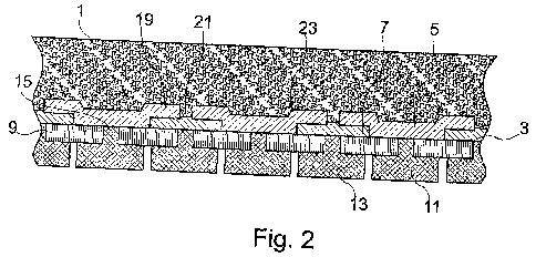
Fig. 2 is a cross-sectional illustration of a rear-contact solar cell
according to a further
embodiment of the present invention with overlap regions produced by the
emitter push
effect.
CA 02708616 2010-06-09
Fig. 3 is a cross-sectional illustration of a rear-contact solar cell
according to a further
embodiment of the present invention with connecting regions formed in edge
regions of the
base regions.
Fig. 4 is a detail-type plan view onto the rear side of the embodiment
illustrated in Fig. 3.
Fig. 5 is a cross-sectional illustration of a rear-contact solar cell
according to a further
embodiment of the present invention in which overlap regions reach close to
the emitter
contacts.
Fig. 6 is a cross-sectional illustration of a rear-contact solar cell
according to a further
embodiment of the present invention with floating base regions.
Fig. 7 shows a rear-contact solar cell according to the prior art.
Fig. 8 shows a further rear-contact solar cell according to the prior art.
All the figures are merely schematic and not true-to-scale. In the figures,
similar or identical
elements are denoted by the same reference numerals.
DETAILED DESCRIPTION OF PREFERRED EMBODIMENTS
The rear-contact solar cell according to the invention shown in cross section
in Fig. 1 has a
semiconductor substrate 1 in the form of a silicon wafer. Both emitter regions
5 and base
regions 7 are formed on the rear side surface 3 of the semiconductor substrate
1. A dielectric
layer 9 made of silicon oxide or silicon nitride, which can serve to passivate
the surface of the
semiconductor substrate and/or as a rear side reflector, but does not
necessarily have to be
electrically insulating, is also located on the rear side surface 3. The
emitter contacts 11 and
the base contacts 13 are then formed over the dielectric layer 9. Both the
emitter and the base
contacts 11, 13 are formed in the form of elongate, finger-shaped contacts
running
perpendicularly to the plane of the drawing. They have substantially the same
widths WE, WB.
The emitter contact 11 contacts an emitter region 5 through line-shaped
openings or through
dot-shaped openings 15, which are adjacently arranged linearly one after
another, in the
dielectric layer 9. The width we of the partial region of the emitter region 5
that adjoins the
rear side surface 3 is slightly greater than the width WE of the corresponding
emitter contact
11. Accordingly, there is no risk of the emitter contact 11 causing a short
circuit to the
adjacent base region 7 even when the dielectric layer 9 is not electrically
insulating.
Similarly, a finger-shaped base contact 13 extends via the dielectric layer 9
and contacts the
CA 02708616 2010-06-09
16
base region 7 positioned thereunder through a line-shaped opening or through
dot-shaped
openings 17 which are adjacently arranged linearly one after another. In this
case too, the
width WB of the base contact 13 is slightly less than the width Wb of the base
region 7
positioned thereunder, so that there is no risk of short circuits between
metal contacts of one
polarity and semiconductor regions of the other polarity, i.e. for example
between base
contacts and emitter regions.
In overlap regions 19, the emitter region 15 overlaps a laterally adjoining
base region 7. This
overlap region 19 is in this regard produced in that, for producing the rear-
contact solar cell
shown, firstly the emitter regions 5 having a comparatively deep depth to were
diffused into
the rear side of the semiconductor substrate 1 and subsequently the base
regions 7 having a
shallower depth tb were diffused-in, the diffusion of the base regions due to
the process
parameters used in this case, such as for example temperature and diffusion
duration, being
carried out in such a way that in the region of the base regions 7
overcompensation of the
emitter doping located there takes place.
The overlap regions 19 have a width wõ which is slightly less than half the
width Wb of the
base regions 7. A small gap, which acts as a connecting region 21 and at which
the
corresponding base region 7 is electrically contacted with the interior of the
semiconductor
substrate I and via which the majority charge carriers produced in the
semiconductor
substrate 1 can flow toward the base contact 13, is thus left between opposing
overlap regions
19.
The embodiment illustrated in Fig. 2 of the rear-contact cell according to the
invention
corresponds in most of its features to the embodiment shown in Fig. 1. The
main difference is
the step-shaped junction 23 which may be seen in the emitter region 5 at the
edge of the
overlap region 19. This junction 23 is produced when the emitter push effect
is utilised during
the production of the emitter regions 5 and the base regions 7 and thus, as
the base region 7
diffuses-in, the emitter region 5 positioned thereover is pushed in the
overlap region 19
deeper into the interior of the semiconductor substrate 1.
The embodiment shown in Figs 3 and 4 of the rear-contact solar cell according
to the
invention differs from the embodiments described hereinbefore mainly in that
the connecting
region 21, which connects the base region 7 arranged on the rear side surface
3 to the interior
of the semiconductor substrate 1, is not arranged roughly in the centre of the
base region 7 as
shown in Figures 1 and 2. Instead, two connecting regions 21 of this type are
provided that
CA 02708616 2010-06-09
17
are each provided in edge regions 25 of the base regions 7 and preferably do
not form long
lines running parallel to the metal contacts, but rather are particularly
preferably dot-shaped
connecting regions. As a result, majority charge carriers, which are produced
in the interior of
the semiconductor substrate 1 in a region above the emitter regions 5, that is
to say between
two laterally adjacent base regions 7, can for example flow away toward the
base contact 13
through the connecting regions 21 provided in the edge region 25, instead of
having to flow,
as in the embodiment shown in Figs 1 and 2, over a longer distance up to the
connecting
region 21 provided in the centre of the base region 7 before they can flow
away to the base
contact 13. Accordingly, serial resistance losses can be reduced as a result.
As a result of the fact that the connecting regions 21 are formed in this
embodiment merely in
a dot-shaped manner, there is also an electrical contact of the regions of the
emitter regions 5
that are arranged centrally over the base contacts 13 to the regions of the
emitter regions 5
that are electrically contacted with the emitter contacts 11. Apart from the
small recesses on
the connecting regions 21, substantially the entire surface of the solar cell
can thus be covered
with an emitter 5, so that charge carriers can be collected very efficiently.
Fig. 5 shows an embodiment in which the emitter regions 5 adjoin the rear side
surface 3
merely in the region of the emitter contacts 11. In the regions positioned
therebetween, the
emitter regions 5 are buried deeper in the interior of the solar cell and
separated from the rear
side surface 3 by base regions 7 positioned therebetween. These base regions 7
are in turn
covered by a dielectric layer 9, preferably a thermal oxide, and are as a
result surface-
passivated very effectively.
Fig. 6 shows an embodiment in which some of the base regions 7 are not
electrically
contacted with base contacts 13. These "floating" base regions 7' are
insulated from the
contacted base regions 7 by parts of the emitter regions 5. The floating base
regions 7' can be
passivated very effectively by a dielectric layer 9 deposited thereon.
Finally, reference is made to the fact that the terms "comprise", "have", etc.
do not rule out
the presence of further elements. The term "a(n)" does not rule out the
presence of a plurality
of items either. The reference numerals in the claims serve merely to improve
readability and
are not in any way intended to restrict the scope of protection of the claims.