Note: Descriptions are shown in the official language in which they were submitted.
CA 02709668 2010-06-15
WO 2009/085994 PCT/US2008/087504
CONNECTIONS FOR ULTRASOUND TRANSDUCERS
RELATED APPLICATIONS
This application claims priority from U.S. Patent Application Serial No.
11/965,178;
filed on December 27, 2007, which is hereby incorporated by reference in its
entirety.
FIELD OF THE INVENTION
The present invention relates to ultrasound transducers, and more particularly
to
connections for ultrasound transducers.
BACKGROUND INFORMATION
An ultrasound transducer is typically fabricated as a stack of multiple layers
that
depend on the application of the transducer. Figures la and lb show typical
ultrasound
transducers. Each transducer comprises, from the bottom up, a backing layer
30, a bottom
electrode layer 17, an active element layer (e.g., piezoelectric element or
PZT) 10, a top
electrode layer 13, a matching layer (or multiple matching layers) 20, and a
lens layer (for
focused transducers) 35 and 45. The lens may be a convex lens 35 or a concave
lens 45. The
backing, matching and lens layers are all passive materials that are used to
improve and
optimize the performance of the transducer. The backing layer is used to
attenuate ultrasound
energy propagating from the bottom of the transducer so that ultrasound
emissions are
directed from the top of the transducer and the matching layer is used to
enhance acoustic
coupling between the transducer and surrounding environment.
In most stacked transducers, the active element (e.g., PZT) must electrically
communicate with a system that drives the active element, receives signals
from the active
element, or both. For ultrasound transducers, the active element converts
electrical energy
into mechanical energy to generate ultrasound waves, and vice versa to sense
ultrasound
waves. This makes the physical connections between the system and the active
element
critical and demanding. In Intravascular Ultrasound (IVUS) applications, the
demands on
these connections may be compounded due to the following reasons: the scale of
operation
may be in the micron range, the ultrasound device may have to meet
sterilization
compatibility requirements, and the ultrasound device may be rotated at high
speeds in
continuously varying anatomy.
SUMMARY OF THE INVENTION
Described herein are electrical connections to acoustic elements, e.g.,
piezoelectric
elements, having lower resistance and reduced signal loss.
In an exemplary embodiment, a transducer comprises an active acoustic element,
a
passive layer attached to the acoustic element, and a conductive post embedded
in the passive
1
CA 02709668 2010-06-15
WO 2009/085994 PCT/US2008/087504
layer to provide a direct low resistance electrical connection to the acoustic
element. In one
embodiment, the conductive post has an exposed side surface allowing
electrical connections
to be made from the side of the transducer. In another embodiment, the
conductive post has
an exposed bottom surface allowing electrical connections to be made from the
bottom of the
transducer.
The conductive post advantageously provides a lower resistance connection to
the
transducer compared with the prior art in which a connection is made to the
transducer
through a housing and/or a backing layer. Further, the conductive post
provides for robust
connections that can withstand exposure to sterilizers at elevated
temperatures during
sterilization of the transducer.
In another embodiment, the transducer comprises an extension substrate
adjacent to
the acoustic element and attached to the same electrode as the acoustic
element. The
extension substrate protects the acoustic element from thermal stress when a
connection is
made to the electrode at high temperatures, e.g., soldering or laser welding.
In one
embodiment, the conductive post is aligned with the extension substrate. When
a lead or
other conductor is connected to the conductive post at high temperatures, the
extension
substrate is subjected to the high temperatures instead of the acoustic
element, thereby
protecting the acoustic element. The lead or other conductor may also be
connected to the
electrode without the conductive post, e.g., by soldering the lead directly to
the electrode. The
extension substrate may comprise silicon, the same material as the acoustic
element, or other
material. In one embodiment, the extension substrate comprises an integrated
circuit for
processing signals to or from the active acoustic element.
Other systems, methods, features and advantages of the invention will be or
will
become apparent to one with skill in the art upon examination of the following
figures and
detailed description. It is intended that all such additional systems,
methods, features and
advantages be included within this description, be within the scope of the
invention, and be
protected by the accompanying claims.
BRIEF DESCRIPTION OF THE FIGURES
In order to better appreciate the above recited and other advantages of the
present
inventions are objected, a more particular description of the invention
briefly described above
will be rendered by reference to specific embodiments thereof, which are
illustrated in the
accompanying drawings. It should be noted that the components in the figures
are not
necessarily to scale, emphasis instead being placed upon illustrating the
principles of the
invention. Moreover, in the figures, like reference numerals designate
corresponding parts
2
CA 02709668 2010-06-15
WO 2009/085994 PCT/US2008/087504
throughout the different views. However, like parts do not always have like
reference
numerals. Moreover, all illustrations are intended to convey concepts, where
relative sizes,
shapes and other detailed attributes may be illustrated schematically rather
than literally or
precisely.
Fig. 1 a shows a prior art ultrasound transducer comprising of a stack of
layers with a
convex lens.
Fig. lb shows a prior art ultrasound transducer comprising of a stack of
layers with a
concave lens.
Fig. 2 shows a perspective view of a transducer comprising a conductive post
for
providing a direct electrical connection to the acoustic element of the
transducer according to
an embodiment of the present invention.
Fig. 3 shows a bottom view of the transducer in Fig. 2.
Fig. 4(a) shows a lead connected to an exposed side surface of the conductive
post
according to an embodiment of the present invention.
Fig. 4(b) shows a lead connected to an exposed bottom surface of the
conductive post
according to an embodiment of the present invention.
Fig. 4(c) shows an integrated circuit (IC) chip connected to the exposed
bottom
surface of the conductive post according to an embodiment of the present
invention.
Figs. 5(a)-5(h) show steps for a batch process for fabricating transducers
according to
an embodiment of the present invention.
Fig. 6(a) and 6(b) show a transducer in which a lead is directly connected to
the
electrode of the acoustic element according to an embodiment of the present
invention.
Fig. 7 shows a transducer comprising an extension substrate adjacent to the
acoustic
element according to an embodiment of the present invention.
Figs. 8(a)-8(h) show steps for a batch process for fabricating transducers
comprising
extension substrates according to an embodiment of the present invention.
Fig. 9 shows a top view of electrodes of a transducer comprising an extension
substrate according to an embodiment of the present invention.
Fig. 10 shows a cross-section view of a transducer comprising an extension
substrate
according to an embodiment of the present invention.
Fig. 11 shows a lead connected to an electrode of a transducer through an
opening in
the matching layer according to an embodiment of the present invention.
Fig. 12 shows a lead connected to an electrode of a transducer through a
conductive
post in the matching layer according to an embodiment of the present
invention.
3
CA 02709668 2010-06-15
WO 2009/085994 PCT/US2008/087504
DETAILED DESCRIPTION
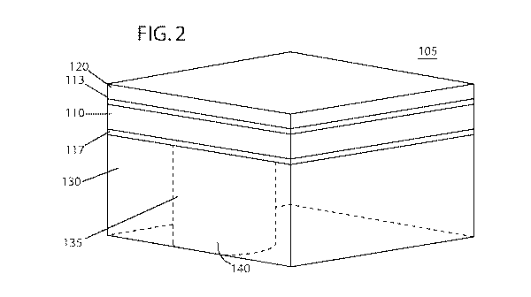
Figures 2 and 3 show an exemplary stacked transducer 105 according to an
embodiment of
the invention. The transducer 105 comprises an active acoustic element 110,
e.g., a
piezoelectric element, and top and bottom electrodes 113 and 117 deposited on
the top and
bottom surfaces of the active element 110, respectively. The electrodes 113
and 117 may
comprise thin layers of gold, chrome, or other conductive material. The
transducer's emitting
face may have a square shape, circular shape, or other shape.
The transducer 105 further comprises a matching layer 120 on top of the active
element 110 and a backing layer 130 on the bottom of the active element 110.
The transducer
105 further comprises a conductive, e.g., metal, post 135 embedded in the
backing layer 130
to provide a direct electrical connection to the active element 110. As
discussed further below,
the conductive post 135 can be fabricated using current microfabrication
techniques, e.g.,
integrated circuit (IC) and MEMS fabrication techniques. In the embodiment
shown in
figures 2 and 3, the conductive post 130 includes an exposed side surface 140,
e.g., a chamfer,
and an exposed bottom surface 145. This allows a lead to be connected to the
conductive post
135 on either the exposed side surface 145 or the exposed bottom surface.
Figure 4(a) shows
an example of the transducer 105 with a lead 150 connected to the side surface
140 of the
post 135, e.g., using solder, epoxy, or laser welding. Figure 4(b) shows an
example of the
transducer 105 with a lead 155 connected to the bottom surface 145 of the post
135. The lead
150 or 155 may be part of a twisted wire pair coupled to an ultrasound system.
Alternatively,
the lead 150 or 155 may be connected at the other end to a coaxial cable
coupled to the
ultrasound system. In the Figures, the backing layer is shown semi-transparent
so that the
embedded conductive post is visible in the Figures.
The conductive post 135 provides a better electrical connection to the active
element 110
with lower resistance compared with prior art methods, in which the lead is
electrically
connected to the active element through a secondary conduction path such as
through the
housing and/or the backing layer. The series resistance can be reduced
considerably
depending on the material used for the post 135, e.g., nickel, gold, copper,
etc., with gold
being the optimal choice from a performance standpoint. Further, the
conductive post 135
improves flexibility in the design of the transducer by increasing the number
of passive
materials that are available to form the transducer. This is because the
choice of passive
materials is no longer limited to conductive materials. Since the conducive
post provides
4
CA 02709668 2010-06-15
WO 2009/085994 PCT/US2008/087504
conduction that is independent of the passive material properties, the passive
materials do not
have to be conductive.
The conductive post 135 provides a more robust connection compared with prior
art
methods. In prior art methods, the backing layer is formed of a conductive
epoxy layer, e.g.,
epoxy with silver filler, that is connected to the lead with epoxy. This
results in an epoxy-to-
epoxy connection between the conductive epoxy of the backing layer and the
epoxy used to
connect the lead to the backing layer. This epoxy-to-epoxy connection is
susceptible to
cracking and separation during transducer sterilization, in which the
transducer is exposed to
a sterilizer, e.g., ethylene oxide sterilizer, at elevated temperatures to
sterilize the transducer.
Connecting the lead to the conductive post 135, e.g., using solder, provides a
more robust
connection that is better able to withstand sterilization than the epoxy-to-
epoxy connection.
Figure 4(c) shows another method of making a connection using the conductive
post
135. In this embodiment, a lead 190 is connected to the conductive post 135
through an
integrated circuit (IC) chip 170. The IC chip 170 comprises a conductive
contact pad 180 for
the post 135 and another conductive contact pad 185 for the lead 190. The
contact pads may
be metal contact pads deposited on the IC chip 170. The contact pad 180 is
bonded to the
bottom surface 165 of the post 135, e.g., using a solder bump (not shown).
Alternatively, the
contact pad 180 may be bonded to the side surface of the post 135. The lead
190 is bonded to
the conductive pad 185. The IC chip 170 contains a conductive path (not show)
beneath an
insulating layer, e.g., silicon oxide or other passivation layer, that
electrically connects the
two pads 180 and 185. The IC chip 170 may be fabricated using well-known IC
fabrication
techniques, e.g., CMOS fabrication techniques. The IC chip 170 may also
contain electronics
for processing signals to and from the transducer, e.g., filters and signal
processors. For
example, the IC chip 170 may contain filters coupled between the contact pads
185 and 180
for filtering out signal noise and/or an amplifier to amplify signals from the
transducer before
they are put on a long cable to the imaging system.
A conductive post may also be embedded in the matching layer 120 to provide an
electrical connection to the active element 110. In an alternative embodiment,
a portion of the
matching layer 120 may be stripped off to expose a small area of the top
electrode 113, and a
lead may be connected directly to the exposed area of the top electrode 113.
In another
alternative embodiment, the matching layer may be made of a conductive
material, e.g., silver
epoxy, with the lead connected to the matching layer.
Although the exemplary embodiments in the Figures show the conductive post 135
having two exposed surfaces, the post 135 may only have an exposed bottom
surface. For
CA 02709668 2010-06-15
WO 2009/085994 PCT/US2008/087504
example, the post may be located within the backing layer with no exposed side
surface.
Alternatively, the post may only have an exposed side surface and not extend
all the way
down to the bottom of the backing layer.
A batch process for fabricating transducers according to an exemplary
embodiment
will now be given with reference to Figures 5(a)-5(h). The batch process is
compatible with
MEMS microfabrication techniques. In this example, the post is made of
deposited metal,
although other conductive materials, e.g., heavily doped silicon, may also be
used.
Figure 5(a) shows an active element layer 210, e.g., a piezoelectric element,
with
electrode layers 213, 217, e.g., gold on chrome electrode. The active element
layer 210 rests
on a carrier 260, e.g., silicon wafer, for supporting the transducer layers
during fabrication. A
layer of light-sensitive photoresist 265, e.g., SU-8 or KMPR, is applied on
top of the active
element 210 using spin coating. The photoresist layer 265 can be either
positive or negative
based on its response to light. Positive photoresist becomes weaker and more
soluble when
exposed to light while negative photoresist becomes stronger and less soluble
when exposed
to light. Photoresists are commonly used in IC and MEMS fabrication with
consistent
repeatable results.
In Figure 5(b), a mask 270, e.g., chrome on glass, is used in conjunction with
light
exposure equipment to form a pattern in the photoresist 265. In this example,
the photoresist
265 is positive and the mask 270 is transparent in areas where the photoresist
265 is to be
removed to form the posts. UV light 275 is filtered through the mask 270 and
reaches the
underlying photoresist 265. The areas of the photoresist 265 corresponding to
the transparent
areas 280 of the mask 270 are exposed to the UV light 275. For the example of
negative
photoresist, the mask would be opaque in areas where the photoresist is to be
removed.
In Figure 5(c), the areas of the photoresist 265 that were exposed to light
are removed
with a developer, e.g., solvent, leaving the desired pattern imprinted in the
photoresist 265.
The areas where the photoresist 265 has been removed forms voids 285 in the
photoresist 265.
Preferably, the bottom of the voids 285 are cleaned to obtain complete
exposure of the
electrode 217 to provide a seed layer for electroplating.
In Figure 5(d) metal is deposited in the voids 285 using electroplating to
form the
posts 235. The posts 235 may be formed of gold, nickel, copper, or other
conductive material.
In Figure 5(e), the photoresist 265 is stripped away leaving the standing
posts on the
electrode 217. In Figure 5(t), the surface is cleaned and a backing layer 230
is applied over
the posts 235 and the exposed electrode 217. The backing layer may be made of
epoxy or
other material that is cast and then cured to form the backing layer. In
Figure 5(g), the
6
CA 02709668 2010-06-15
WO 2009/085994 PCT/US2008/087504
backing layer 230 is ground down to remove excess backing material and obtain
a flat
backing surface.
In Figure 5(h), the transducer layers are flipped over on the carrier 260. The
matching
layer 220 is applied to the active element layer 210. The transducer layers
are then diced to
release individual transducers 205. A dicing saw cuts through the transducer
layers and
partially into the carrier 260 to release the individual transducers 205. In
this embodiment, the
dicing saw also partially cuts through portions of the posts 235 to form the
exposed flat side
surfaces 240 of the individual transducers.
Figures 6(a) and 6(b) show an alternative method for making a connection to
the active
element 110. In this embodiment, a void 335 is formed in the backing layer 130
to expose an
area of the electrode 117. Instead of filing the void with metal to form a
metallic post, the
lead 350 is connected directly to the exposed area of the electrode 117
through the void 335,
e.g., using solder, epoxy, or the like. After the lead 350 is connected to the
electrode 117, the
void 335 can be filled with the same passive material (not shown) used for the
backing layer
130 to maintain uniformity. In this embodiment, the backing layer 130 may be
made of a
material that can be easily dissolved, e.g., wax or photoresist, to form the
void. For example,
for a backing layer 130 comprising a photoresist layer, the photoresist layer
may be exposed
to UV light through a mask having a pattern that defines the void. The light
exposure through
the filter transfers the mask pattern defining the void to the photoresist
layer. After light
exposure, the photoresist layer may be selectively dissolved to form the void
335, e.g., using
a developer, based on the transferred pattern.
Figure 7 shows a transducer 405 according to another exemplary embodiment of
the
invention. In this embodiment, the transducer 405 comprises an extension
substrate 450 at the
same level as the active element 410 and having the same thickness. The
extension substrate
450 may be made of the same material as the active element 410 or different
material. The
extension substrate 450 may be separated from the active element 410 by a gap
455, e.g.,
filled with epoxy. The transducer 405 further comprises top and bottom
electrodes 413 and
417, a matching layer 420, a backing layer 430, and a conductive, e.g., metal,
post 435
embedded in the backing layer 430. The conductive post 435 is connected to the
bottom
electrode 417 and aligned with the extension substrate 450. Preferably, the
extension
substrate 450 is made of a material with favorable properties for making
electrical
connections. For example, silicon may used for the extension substrate 450
because of its
excellent electrical properties and stability, and the well developed
integrated processing for
silicon at the miniaturization level.
7
CA 02709668 2010-06-15
WO 2009/085994 PCT/US2008/087504
The extension substrate 450 reduces the risk of damage to the active element
410
when connections are made to the electrodes 413 and 417. For example, when a
lead 460 is
soldered to the post 435, the region around the post 435 is raised to a high
temperature. By
aligning the post 435 with the extension substrate 450 instead of the active
element 410, the
extension substrate 450 is subjected to the high temperatures and thermal
stress associated
with soldering instead of the active element 410, thereby protecting the
active element 410.
This is important because high temperatures, thermal shock and similar
conditions can cause
several failure modes in piezo materials such as depoling (which irreversibly
destroys the
piezo properties of the material) cracking, and reduced material integrity. By
protecting the
active element 410, the extension substrate 450 reduces the risk of damage to
the active
element 410. Further, the extension substrate 450 allows more robust
connection techniques
to be used that would otherwise not be possible due to the sensitivity of
piezo materials to
high temperatures, thermal shock and similar conditions.
A batch process for fabricating transducers with extension substrates
according to an
exemplary embodiment will now be given with reference to Figures 8(a)-8(h).
The batch
process is compatible with MEMS microfabrication techniques. In this example,
the post is
made of deposited metal, although other conductive materials, e.g., heavily
doped silicon,
may also be used.
Figure 8(a) shows active elements 510, e.g., a piezoelectric elements, lying
on a
photoresist layer 580 and a carrier substrate 585. The active elements 510 may
be formed by
dicing a piezo wafer into individual piezo elements. Figure 8(a) also shows a
silicon wafer
570 with the extension substrates 550 etched into the wafer and corresponding
to the spaces
575 between the active elements 510. The silicon 570 can be fabricated using
well-known
CMOS microfabrication techniques to form the extension substrates 510.
In Figure 8(b), the extension substrates 550 of the silicon wafer 570 are
aligned with
the spaces between the active elements 510. The silicon wafer 570 is then
overlaid onto the
active elements 510 with the extension substrates 510 inserted between the
active elements
510. The silicon wafer 570 is held in place using a filer epoxy.
In Figure 8(c), the unused portion of the silicon wafer is lapped off to reach
the
desired active element thickness. In Figure 8(d) , a first electrode layer
517, e.g., gold on
chrome, is deposited, e.g., sputtered, on the active elements 510 and
substrate extensions 550.
In Figure 8(e), a backing material is cast on the electrode layer 517, and
then cured to form
the backing layer 530. The backing layer 530 may be made of epoxy, polymer or
other
material. In Figure 8(t), the active elements 510 and substrate extensions 550
are released
8
CA 02709668 2010-06-15
WO 2009/085994 PCT/US2008/087504
from the carrier 585 by dissolving the photoresist layer 580, and flipped over
so that the
backing layer 530 is below. A second electrode layer 513, e.g., gold on
chrome, is deposited,
e.g., sputtered, on the active elements 510 and substrate extensions 550. In
Figure 8(g), a
matching layer 520 is deposited on the second electrode layer 513. The
matching layer 520
may be spin coated on the electrode layer 513. In Figure 8(h), the matching
layer 520,
electrodes 513 and 517, silicon 550, and backing layer 520 are diced, e.g.,
using a dicing saw,
to separate the transducers. The backing layers of the individual transducers
may then be cut
away from the main backing layer to release the transducers.
Metal posts can be embedded in the backing layers of the transducers by
including
additional process steps based on the process shown in Figures 5(a)-5(h). For
example, metal
posts can be embedded in the backing layer 530 by adding the process steps for
forming the
metal posts in steps 8(d) and 8(e) and casting the backing layer 530 on the
metal post.
When silicon or other semiconductor is used for the extension substrate, an
integrated
circuit can be fabricated on the extension substrate, e.g., using a CMOS
process. The
integrated circuit can include, e.g., filters for filtering signals, an
amplifier for amplifying
signals from the transducer, and other processing electronics. Placing an
integrated circuit
next to the transducer can reduce signal noise and/or signal loss caused by
the long cable
from the transducer to the imaging system and can reduce the amount of
processing that
needs to be done at the system side.
Figs. 9 and 10 illustrate an extension substrate, e.g., silicon extension
substrate, with
an integrated circuit according to an embodiment of the invention. In this
example, the circuit
is integrated on the top of the extension substrate 650, although it is to be
understood that the
circuit may also be integrated on the bottom. Fig. 9 shows a top view of
electrodes 613a,
163b placed over the extension substrate 650 and the active acoustic element
610. Fig. 10
shows a cross-sectional view of the transducer with the matching layer removed
for ease of
illustration. The top electrode comprises a first electrode 613a overlapping
the extension
substrate 650 and the active element 610 and a second electrode 613b over the
extension
substrate 650 and separated from the first electrode 613a by an isolation gap
663. The
electrodes may be patterned using well-known microfabrication techniques,
e.g., metal
etching. Fig. 10 also shows an example of circuit blocks 670a, 670b integrated
on the
extension substrate 650 and interconnected by conductive traces 665, e.g.,
metal traces. The
circuits may be fabricated using well-known CMOS fabrication techniques, which
can be
used to fabricate filters, amplifiers, and other electronics to process
signals to and from the
9
CA 02709668 2010-06-15
WO 2009/085994 PCT/US2008/087504
active element 610. The layout of the circuit blocks 670a, 670b shown in Fig.
9 is exemplary
only as other layouts may be used.
Referring to Fig. 10, the first electrode 613a is electrically connected to
the integrated
circuits by a via 685a and traces 665, 690a. Trace 690b connects to trace 665
at point 675a.
The first electrode 613a electrically connects the extension substrate 650 to
the active
element 610. The second electrode 613b is electrically connected to the
integrated circuits by
a via 685b and traces 690b, 665. Trace 690b connects to the trace 665 at point
675b. In this
example, the traces 665 and 690a, 690b are underneath a thin passivation
layer, e.g., oxide, of
the extension substrate 650 with the vias 685a, 685b interconnecting the
electrodes 613a,
613b to the lower level traces 690a, 690b. The vias 685a, 685b may be made of
metal or
other conductive material. In Fig. 10, the electrodes 613a, 613b are shown
semi-transparent
so that the underlying extension substrate 650 and active element 610 are
visible in Fig. 10.
Fig. 11 shows an example of a lead 695 electrically connected to the second
electrode
613b through an opening in the matching layer 620. The matching layer 620 may
be striped
away or masked off to form the opening. The other end of the lead may be
connected to a
twisted wire pair or a coaxial cable for coupling electrical signals between
the transducer and
an ultrasound imaging system. Fig. 12 shows another example of a lead 696
electrically
connected to the second electrode 613b through a conductive, e.g., metal, post
697 deposited
on the electrode 613b. The conductive post 697 may be fabricated using similar
techniques
used to fabricated the post embedded in the backing layer. In Figs. 11-12, the
electrodes 613a,
613b, and matching layer 620 are shown semi-transparent so that the underlying
extension
substrate 650 and active element 610 are visible in the Figs. 11-12.
During operation, an electrical signal, e.g., transmit pulse, to the
transducer travels
through the second electrode 613b, the via 685b, and traces 690b, 665 to the
integrated circuit
670a, 670b on the extension substrate 650. The integrated circuit 670a, 670b
may process the
signal or pass the signal without processing it. The signal then travels
through the traces 665,
690a, via 685a, and the first electrode 613a to the active element 610. An
electrical signal
from the active element 610 may also travel through the integrated circuit
670a, 670b for
processing, e.g., amplification, filtering or the like, before traveling down
the long cable to
the ultrasound imaging system. The active element 610 may produce this signal
in response
to a return ultrasound wave received by the active element 610.
In the foregoing specification, the invention has been described with
reference to specific
embodiments thereof. It will, however, be evident that various modifications
and changes
may be made thereto without departing from the broader spirit and scope of the
invention.
CA 02709668 2010-06-15
WO 2009/085994 PCT/US2008/087504
For example, the reader is to understand that the specific ordering and
combination of process
actions described herein is merely illustrative, and the invention can be
performed using
different or additional process actions, or a different combination or
ordering of process
actions. As a further example, each feature of one embodiment can be mixed and
matched
with other features shown in other embodiments. Additionally and obviously,
features may be
added or subtracted as desired. Accordingly, the invention is not to be
restricted except in
light of the attached claims and their equivalents.
11