Note: Descriptions are shown in the official language in which they were submitted.
CA 02709965 2010-09-02
METHOD AND SYSTEM FOR REDUCING COMMON MODE SIGNAL
GENERATION WITHIN A PLUG/JACK CONNECTION
Technical Field
100021 The present invention relates generally to electrical connectors, and
more particularly to a
modular communication jack design with crosstalk compensation that suppresses
crosstalk
present betwccn conductors within a jack and/or plug.
Backeround
[0003) In an electrical communication system, it is sometimes advantageous to
transmit
information (video, audio, data) in the form of differential signals over a
pair of wires rather than
a single wire, where the transmitted signal comprises the voltage difference
between the wires
without regard to the absolute voltages present. Each wire in a wire-pair is
capable of picking up
electrical noise from outside sources, e.g., neighboring data lines.
Differential signals may be
advantageous to use due to the fact that the signals are less susceptible to
these outside sources.
[0004) When using differential signals, it is well known that it is desirable
to avoid the
generation of common mode signals. Common mode signals are related to a
balance of the
transmission line. Balance is a measure of impedance symmetry in a wire pair
between
individual conductors of the wire and ground. When the impedance to ground for
one conductor
is different than the impedance to ground for the other conductor, then
differential mode signals
are undesirably converted to common mode signals.
(00051 Another concern with differential signals is electrical noise that is
caused by neighboring
differential wire pairs, where the individual conductors on each wire pair
couple (inductively or
capacitively) in an unequal manner that results in added noise to the
neighboring wire pair. This
is referred to as crosstalk. Crosstalk can occur on a near end (NEXT) and a
far end (FEXT) of a
transmission line. It can also occur internally between differential wire
pairs in a channel
(referred to as internal NEXT and internal FEXT) or can couple to differential
wire pairs in a
CA 02709965 2010-06-17
WO 2009/085986 PCT/US2008/087486
neighboring channel (referred to as alien NEXT and alien FEXT). Generally
speaking, so long
as the same noise signal is added to each wire in the wire-pair, then the
voltage difference
between the wires will remain about the same and crosstalk is minimized.
[0006] In the communications industry, as data transmission rates have
steadily increased,
crosstalk due to undesired capacitive and inductive couplings among closely
spaced parallel
conductors within the jack and/or plug has become increasingly problematic.
Modular
connectors with improved crosstalk performance have been designed to meet the
increasingly
demanding standards. For example, recent connectors have introduced
predetermined amounts
of crosstalk compensation to cancel offending NEXT. Two or more stages of
compensation are
used to account for phase shifts from propagation delay resulting from a
distance between a
compensation zone and the plug/jack interface, which, in turn gives the system
an increased
bandwidth. Additionally, new standards have been particularly demanding in the
area of alien
crosstalk. Common mode signals are known to radiate more than differential
signals, and
therefore are a major source of alien crosstalk. Therefore, minimizing any
sort of common mode
signal is desirable, and this has driven the need for new connector designs.
[0007] Recent transmission rates, including those requiring a bandwidth in
excess of 250 MHz,
have exceeded the capabilities of the prior techniques for both internal NEXT
and alien NEXT.
Thus, improved compensation techniques are needed.
Summary
[0008] Within embodiments disclosed below, a communication connector is
described that
includes a plug and a jack, into which the plug is inserted. The plug
terminates a length of
twisted pair communication cable. The jack includes a sled arranged to support
interface
contacts for connecting to wires within the twisted pair communication cable,
a rigid circuit
board that connects to the interface contacts, and a flex board that contacts
the plug interface
contacts.
[0009] The structure of the plug creates crosstalk that is then compensated
for by the jack.
Additionally, the unbalanced structure of the plug can create common mode
signals that may be
detrimental to alien crosstalk performance. Crosstalk can be added by the flex
board and rigid
board in order to compensate for the crosstalk from the plug. The crosstalk
can be added in such
2
CA 02709965 2015-06-29
a way that the crosstalk allows for internal NEXT and FEXT to pass at
frequencies
exceeding 500 MHz, while at the same time minimizing the creation of common
mode signals, which ultimately improves alien crosstalk performance.
In some embodiments of the invention, there can be provided a
communication connector comprising:
a plug that terminates a length of twisted pair communication cable; and
a jack, into which the plug is inserted, the jack supporting interface
contacts
for connecting to wires within the twisted pair communication cable, and
including
circuitry to minimize internal near end crosstalk and internal far end
crosstalk
between the wires in the twisted pair communication cable, and to minimize
differential mode to common mode and common mode to differential mode signal
conversion within a mated plug/jack combination wherein the twisted pair
communication cable includes eight wires numbered 1-8, and is arranged as four
twisted wire pairs numbered wire pairs 12, 45, 36 and 78, so that while in a
twisted
pair configuration, wires numbered 1 and 2 are twisted, wires 4 and 5 are
twisted,
wires 3 and 6 are twisted and wires 7 and 8 are twisted, and at a termination
point in
the plug, the wires are untwisted and positioned adjacent one another in the
order
from wire 1 to wire 8 and wherein a capacitance between traces carrying
signals of
wires 1 and 3, a capacitance between traces carrying signals of wires 2 and 6,
a
capacitance between traces carrying signals of wires 2 and 3, and a
capacitance
between traces carrying signals of wires 1 and 6 are all about equal to each
other.
In some embodiments of the invention, there can be provided a mated
plug/jack combination including contacts for connecting to wires within a
twisted pair
communication cable, wherein the twisted pair communication cable includes
eight
wires numbered 1-8, and is arranged as four twisted wire pairs numbered wire
pairs
12, 45, 36 and 78, so that while in the twisted pair configuration, wires
numbered 1
and 2 are twisted, wires 4 and 5 are twisted, wires 3 and 6 are twisted and
wires 7 and
8 are twisted, and at a termination point in the plug, the wires are untwisted
and
positioned adjacent one another in the order from wire 1 to wire 8, and
wherein the
3
CA 02709965 2015-06-29
mated plug/jack combination includes capacitance between contacts of wires 1
and 3
(C13), contacts of wire 2 and 6 (C26), contacts of wire 2 and 3 (C23), and
contacts of
wires 1 and 6 (C16), wherein all the capacitances are about equal.
[0010] These and other aspects will become apparent to those of ordinary skill
in the
art by reading the following detailed description, with reference where
appropriate to
the accompanying drawings. Further, it should be understood that the
embodiments
noted herein are not intended to limit the scope of the invention as claimed.
Brief Description of Figures
[00111 Figure 1 illustrates an example of a transmission channel used to
transmit
information (video, audio, data) in the form of electrical signals over
cabling.
[0012] Figure 2 illustrates an example conceptual cable that includes wires 1-
8
illustrated in a manner as the wires are laid out in a plug.
[00131 Figure 3 is an exploded perspective illustration of an example
communication
connector that includes a plug and a jack, into which the plug may be
inserted.
[0014] Figure 4 illustrates a side view of an example of a sled and PCB rigid
board
configuration including interface contacts and IDCs.
[0015] Figure 5 illustrates a portion of an example plug contacting interface
contacts
of a jack.
[0016] Figure 6 illustrates a rear view of an example of the jack with the
IDCs
numbered to correspond to wire number pinouts on the PCB rigid board.
[0017] Figure 7A illustrates examples of conceptual differential signals
transmitted
along wire pairs 12 and 36.
[0018] Figure 7B illustrates examples of conceptual differential signals
transmitted
along wire pairs 36 and 78.
[0019] Figure 8 illustrates how common mode generation from a plug/jack
connection creates alien crosstalk seen in a channel.
[0020] Figure 9 illustrates an example plug blade layout with the blades
numbered
according to the number of the wire that terminates to the blade.
3a
CA 02709965 2010-06-17
WO 2009/085986 PCT/US2008/087486
[0021] Figure 10 illustrates an example schematic diagram showing capacitances
between wire
pairs 36, 12, and 78 of a plug/jack designed to optimize internal NEXT, FEXT,
and to reduce
common mode creation for wire pair combinations 36-12 and 36-78.
[0022] Figure 11 illustrates an example schematic diagram showing capacitances
added between
wire pair combination 45-36.
[0023] Figure 12 illustrates an example layout of a flex board of a jack
designed to optimize
internal NEXT and reduce the common mode creation on wire pairs 12 and 78.
[0024] Figure 13 illustrates an enlarged example layout view of the rigid
board from Figure 3.
[0025] Figure 14 illustrates an example layout of the rigid board showing a
top layer, a first
inner layer, a second inner layer, and a bottom layer.
[0026] Figures 15A-F show example views of the different layers of the rigid
board.
[0027] Figures 16A-B illustrate example standard laboratory tests performed to
illustrate benefits
of the present application.
Detailed Description
[0028] The present application describes a communication connector that
includes a plug and a
jack, into which the plug is inserted. The jack includes circuitry to
compensate for crosstalk
between wire pairs of the plug by adding capacitance and mutual inductance
between wires of
the wire pairs.
[0029] Referring now to the figures, Figure 1 illustrates a transmission
channel 100 used to
transmit information (video, audio, data) in the form of electrical signals
over wire. The system
is shown to include a switch 102, at which a patch cable 104 connects a plug
106/jack 108
connection at a patch panel 110. At the patch panel 110, the information may
be routed through
patch cable 112 to another plug 114/jack 116 connection at a second patch
panel 118, for
example. From there, the information may be routed over a long distance, e.g.,
85 m, via a wire
120 to a plug 122/jack 124 connection that is present within a patch panel,
for example. From
the patch panel, the information is routed over a patch cable 126 to a plug
128/jack 130
connection. The plug/jack connections in Figure 1 may be a registered jack
(RJ) standardized
physical interface for connecting telecommunications equipment or computer
networking
4
CA 02709965 2010-06-17
WO 2009/085986 PCT/US2008/087486
equipment. For example, the plug/jack connections may be RJ45 connections of
the modular or
punchdown connector type.
[0030] The connections shown in Figure 1 may be compatible with Category 6A
cabling,
commonly referred to as Cat 6A, which is a cable standard for 10-Gigabit
Ethernet and other
network protocols that is backward compatible with the Category 6, Category
5/5e, and Category
3 cable standards. Category 6A features more stringent specifications for
crosstalk and system
noise, which can be particularly difficult for UTP solutions to pass. The
cable standard provides
performance of up to 500 MHz and is suitable for 10BASE-T/100BASE-TX, 1000BASE-
T
(Gigabit Ethernet), and 10GBASE-T (10-Gigabit Ethernet).
[0031] Thus, the cables shown in Figure 1 may each include four twisted copper
wire pairs as
laid out in a standard RJ45 plug. Figure 2 illustrates a cable 200, which
includes wires 1-8. In
the configuration shown in Figure 2, wires 1 and 2 are a twisted pair, wires 4
and 5 are a twisted
pair, wires 3 and 6 are a twisted pair, and wires 7 and 8 are a twisted pair.
Thus, there is
overlapping between the 4 to 5 pair and the 3 to 6 pair, which adds
significant crosstalk to pair
combination 45-36. The wires 1-8 terminate at a plug 202, at which point the
wires are
untwisted.
[0032] The cable 200 includes twisted wire pairs for the purposes of
minimizing electromagnetic
interference (EMI) from external sources, electromagnetic radiation from the
unshielded twisted
pair (UTP) cable, and crosstalk between neighboring pairs.
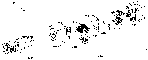
[0033] Figure 3 is an exploded perspective illustration of a communication
connector 300 that
includes a plug 302 and a jack 304, into which the plug 302 may be inserted.
The plug 302
terminates a length of twisted pair communication cable (not shown), while the
jack 304 may be
connected to another twisted-pair communication cable (not shown in Figure 3).
[0034] As shown from left to right, the jack 304 includes a main housing 306
and a bottom front
sled 308 and top front sled 310 arranged to support eight plug interface
contacts 312. The plug
interface contacts 312 engage a PCB (Printed Circuit Board) 314 from the front
via through-
holes in the PCB 314. As illustrated, an IDC (Insulation Displacement Contact)
support 315
allows eight IDCs 316 to engage the PCB 314 from the rear via additional
through-holes in the
PCB 314. A rear housing 318 that has passageways for the IDCs 316 serves to
provide an
interface to a twisted pair communication cable.
CA 02709965 2010-06-17
WO 2009/085986 PCT/US2008/087486
[0035] Figure 4 illustrates a side view of the sled 310 and PCB rigid board
314 configuration
including the plug interface contacts 312 and the IDCs 316. Figure 4
illustrates that the sled 310
also includes a flex board 320, which contacts the interface contacts 312 and
contains circuitry to
compensate for crosstalk. The flex board 320 may be a flexible PCB that
includes capacitance
and inductance to compensate for crosstalk. Figure 5 illustrates a portion of
the plug 302
contacting the interface contacts 312. Figure 6 illustrates a rear view of the
jack (PCB rigid
board 314 is hidden from view) with the IDCs numbered to correspond to the
wire number
pinouts on the PCB rigid board 314.
[0036] Within the transmission system 100 in Figure 1, data may be sent over
the wires using
differential signaling, which is a method of transmitting information
electrically by means of two
complementary signals sent on two separate wires. Using the cable shown in
Figure 2, the two
complementary signals are sent over the wire pairs, e.g., over the 1 to 2 pair
("12 pair"). At the
end of the connection of the wire, a receiving device reads a difference
between the two
complementary signals. Thus, any noise equally affecting the two wires will be
cancelled
because the two wires have similar amounts of electromagnetic interference.
Differential mode
transmission radiates less than common mode transmission.
[0037] In a typical transmission system, the cabling is more susceptible to
common-mode
crosstalk than differential mode crosstalk from other cables. A common-mode
signal is one that
appears in phase and with equal amplitudes on both lines of a two-wire cable
with respect to a
local common or ground. Such signals can arise, for example, from radiating
signals that couple
equally to both lines, a driver circuit's offset, a ground differential
between the transmitting and
the receiving locations, or unbalanced coupling between two differential
pairs.
[0038] Using configurations of the cable as discussed herein, alien crosstalk
(e.g., signal
coupling from adjacent channels) from wire pairs in one cable to wire pairs in
another cable can
cause the system to fail requirements for CAT6A (EIA/TIA-568 or ISO). It is
possible that
adjacent channels can have significant common mode alien coupling that will
occur on a UTP
cable that is situated on a front end between the jacks. The common mode
signal can be created
by the plug-jack combination. Current CAT6A component requirements on a plug
or jack may
not be sufficient in reducing the common mode signals that can be generated in
a plug/jack
6
CA 02709965 2010-06-17
WO 2009/085986 PCT/US2008/087486
connection. Hence, a plug/jack that is compliant with the CAT6A standard can
still create a
channel or permanent link that will fail alien crosstalk requirements.
[0039] A standard RJ45 plug adds crosstalk into a signal that needs to be
compensated for by the
jack. On wire pairs 36-12 and 36-78, a crosstalk signal is added mainly by the
plug by wire 2
coupling with wire 3, and wire 6 coupling with wire 7. This is due to a layout
of the plug that
has wire 3 next to wire 2, and wire 6 next to wire 7 (e.g., see Figure 2).
[0040] Figure 7A illustrates conceptual differential signals transmitted along
wire pairs 12 and
36. As shown, using differential signaling, the signal sent along wire 1 is
180 degrees out of
phase with the signal sent along wire 2. The same occurs with the signals
transmitted across
wires 3 and 6. Due to the layout of the wires in a cable, there is crosstalk
caused by the plug
between wires of each pair that have signals of one phase (e.g., wires 1 and
3, and wires 2 and 6),
and between wires of each pair that have signals of an opposite phase (e.g.,
wires 1 and 6, and
wires 2 and 3). To compensate for crosstalk caused by the plug, compensation
is added that is of
a polarity opposite the crosstalk caused by the plug, so that the crosstalk
caused by the plug
between wires of each pair that have signals in phase cancels with crosstalk
caused by the plug
between wires of each pair that have signals out of phase. Thus, it is desired
to create a situation
where together the plug and jack have:
X13 + X26 ¨ X23 ¨ X16 Z 0 (Equation 1)
for wire pairs 36-12, where X13 is compensating crosstalk added between wires
1 and 3, X26 is
compensating crosstalk added between wires 2 and 6, X23 is crosstalk by the
plug between wires
2 and 3, and X16 is crosstalk between wires 1 and 6.
[0041] In addition, the same situation occurs for wire pairs 36-78, as shown
in Figure 7B, and
thus it is desired to create a situation where together the plug and jack
have:
X68 + X37 X67 X38 Z 0 (Equation 2)
where X68 is compensating crosstalk added between wires 6 and 8, X37 is
compensating crosstalk
added between wires 3 and 7, X67 is crosstalk between wires 6 and 7, and X38
is crosstalk
between wires 3 and 8. Note that the Xmay refer to capacitive and/or inductive
crosstalk. The
reason every equation is written as approximately zero is that while being
equal to exactly zero is
desired, most of the time the actual value is around the magnitude of below
¨75 dB at
7
CA 02709965 2010-06-17
WO 2009/085986 PCT/US2008/087486
frequencies below 10 MHz due to the dynamic range of the test equipment,
imperfections in the
assembly process, and the use of different types of plugs.
[0042] In CAT6 and CAT6A specifications, additional crosstalk is generally
time-delayed with
respect to first stage compensating capacitors (X13, X26 and X68, X37). The
crosstalk is of the same
polarity to the plug (X23, X16 and X67, X38). The second crosstalk generally
results in the addition
of a null that increases the bandwidth of the system. Equations 1 and 2 are
still met for this to
work. For more information regarding time-delay signal compensation, the
reader is referred to
U.S. Patent No. 5,997,358, the contents of which are entirely incorporated by
reference, as if
fully set forth herein.
[0043] An additional source of crosstalk is alien crosstalk (e.g., signal
coupling from adjacent
channels). The plug/jack interface is a source of the signals that ultimately
cause alien crosstalk.
For example, an imbalance in the plug blade layout with respect to wire pairs
36-12 and 36-78
creates common mode signals. Wires 3 and 2 are close to each other and wires 6
and 7 are close
to each other, and therefore a differential signal on pair 36 generates a
strong common mode
signal on wire pairs 12 and 78. The common mode signals on wire pairs 12 and
78 couple
between adjacent cables on adjacent channels. These common mode signals on
wire pairs 12
and 78 on the adjacent channel then become converted back into a differential
signal on wire pair
36 that is the alien crosstalk.
[0044] To be compliant to the Telecommunications Industry Association (TIA)/
Electronic
Industries Alliance (EIA) CAT6A specifications and ISO standards, the plug
should have a de-
embedded crosstalk value in a specific range for each pair combination. For
example, for pair
combination 12 to 36 and 36 to 78, the value is:
[0045] 46.5 ¨ 20log(f /100)dB TotalXtalk 49.5 ¨ 20log(f /100)dB (Equation 3)
[0046] where TotalXtalk is the de-embedded crosstalk for pair combinations 12
to 36 and 36 to
78 in dB, and f is a frequency in MHz.
[0047] The total crosstalk for pairs 12 and 36, and 36 and 78 that creates the
de-embedded value
defined as TotalXtalk in Equation 3 can be viewed as that in Equations 1-2
above. Because of
the layout of the plug where the blades for 2 and 3 are next to each other and
6 and 7 are next to
each other,
8
CA 02709965 2010-06-17
WO 2009/085986 PCT/US2008/087486
X23 >> Xi 6 (Equation 4)
and
X67 >> X38 (Equation 5)
It is the imbalance on X12-36 and X36-78 that creates a strong common mode
signal on wire pairs 12
and 78.
[0048] Figure 8 illustrates how common mode signals created at a plug/jack
connection will
create alien crosstalk. Initially a differential signal is injected onto
Channel A (e.g., a first
cable). The plug/jack combinations on Channel A will convert the differential
signal into a
common mode signal. This "mode conversion" (e.g., conversion from a
differential signal to a
common mode signal or a common mode signal into a differential signal) occurs
predominantly
due to a configuration of the blades on the plug and/or how the compensation
for the plug is
performed in the jack.
[0049] The common mode signal also couples over as an alien crosstalk signal
onto the patch
cable of Channel B. The coupling of common mode signals on cabling is not
covered in CAT6A
standards, and hence is usually at a much stronger level than differential
coupling. On Channel
B, the plug-jack combinations convert the common mode signal back into a
differential signal
which causes alien crosstalk on Channel B.
[0050] Thus, two problems exist: the generation of common mode signals by the
plug/jack
connection and the coupling of these signals in the cabling. Hence, factors
influencing the total
amount of alien crosstalk caused by the plug/jack mode conversion include the
mode conversion
from differential to common mode and common mode back to differential, and the
level of
coupling between adjacent cables for the common mode signal. It is desirable
to reduce the
amount of mode conversion in the plug/jack connection.
[0051] In one embodiment, in addition to meeting the requirements of Equations
1 and 2 above,
new requirements are needed to reduce mode conversion. Hence, the values of
the added
crosstalk within the plug/jack combination (capacitance and inductance values)
are generally as
shown below:
C13 '''''''' C= 26 ''''''' C= 23 7."'' C= 16 (Equation 6)
C68 7."'' C= 37 7."'' C= 67 7."'' C= 38 (Equation 7)
9
CA 02709965 2010-06-17
WO 2009/085986 PCT/US2008/087486
M26 7.7:'' M23 7.::'' M16 (Equation 8)
and
M37 7.::'' M67 7.::'' M38 (Equation 9)
where C refers to the total capacitive coupling and Mrefers to the total
mutual inductive
coupling of a mated plug/jack combination. If Equations 6-9 are met, the total
amount of mode
conversion that creates the 12/78 common mode signals from a 36 differential
signal would be
minimized. Creating a jack that is close to meeting equations 6, 7, 8, and 9
can be difficult due
to the fact that the structure of the jack itself adds in inductive and
capacitive components that
are difficult to quantify. Note that while these equations shown balanced
coupling required for
pair combinations 36-12 and 36-78, these balanced requirements are needed for
all pairs (45-36,
45-12, 45-78, and 12-78).
[0052] Referring to Figures 3-5, within the present application, capacitive
crosstalk can be added
in both the flex board 320 and the PCB rigid board 314 of the jack 304. To
optimize mode
conversion, capacitance compensation is added between wires 1 and 3 and wires
2 and 6 to
compensate for the plug crosstalk on the pair combination 12-36, and
compensation can be
added between wires 3-7 and 6-8 to compensate for the plug crosstalk on the
pair combination
36-78 in order for the plug/jack to be compliant with internal NEXT
specifications. For
example, equal capacitance can be added between wires 1-3 and 2-6, and between
wires 3-7 and
6-8 to satisfy Equations 6-7. Figure 9 illustrates a plug blade layout, with
the blades numbered
according to the number of the wire that terminates to the blade.
[0053] To tune for Internal NEXT and mode conversion at the same time in the
jack, the
capacitances C13, C26, C68, and C37 are made to be substantially equal in
magnitude. Likewise,
capacitances C68 and C37 are made to be substantially equal in magnitude.
Capacitors of the
same polarity as the crosstalk from the plug, time-delayed with respect to the
above capacitors
are added in the form of C16 and C38.
[0054] Therefore, the plug/jack compensation to tune for mode conversion and
internal NEXT
for wire pair combinations 36-12 and 36-78 may be that as shown in Figure 10.
As shown, the
plug, due to its geometry, primarily supplies capacitances C23 and C67, which
are equal in value.
The plug also supplies capacitances C13 and C68 that are equal in value. Note
that the plug is also
shown to include capacitances C37, C38, C26, and C16 that are equal in value;
however, these
CA 02709965 2010-06-17
WO 2009/085986 PCT/US2008/087486
capacitances are theoretical values that are not physically added into the
plug, but rather shown
to illustrate that they may be present due to the design of the plug.
[0055] A nose of the jack (e.g., bottom front sled 308, top front sled 310 and
interface contacts
312 altogether) supplies capacitances C13 and C68 due to its geometry, as well
as capacitances C67
and C23. Capacitances C26, C37, C16, and C38 are theoretically present within
the nose and are
shown for completeness. The flex board adds capacitances C26 and C37, which
are equal in
value. The rigid board adds capacitances C16 and C38, and capacitances C68 and
C13.
Capacitances C67, C37, C26, and C23 are theoretical capacitances shown for
completeness. To the
right of the rigid board as shown in Figure 10, within the IDCs, capacitances
C67, C68, C13, and
C23 are added. Figure 10 illustrates example values for each capacitance,
however, other values
may also be used. In addition, the values shown in Figure 10 satisfy Equations
6 and 7 to within
in about 0.1pF.
[0056] Figure 11 illustrates wire pair capacitances for wire pairs 34, 35, 46,
and 56. Using the
same methods as above, it is desired to create a situation where
X34 + X56 ¨ X46 ¨ X35 Z 0 (Equation 10)
where X34 is compensating crosstalk added between wires 3 and 4, X56 is
compensating crosstalk
added between wires 5 and 6, X46 is crosstalk between wires 4 and 6, and X35
is crosstalk
between wires 3 and 5.
[0057] As shown in Figure 11, the plug has capacitances C34, C56, C35, and
C46. The nose of the
jack has capacitances C34, C56, C35, and C46 added to compensate for the net
crosstalk caused by
the plug. The flex board has capacitances C35 and C46 added to compensate for
crosstalk. The
rigid board has C34, C565 C355 and C46 added to compensate for crosstalk.
Therefore any mode
conversion with respect to pair combination 45 and 36 is minimized as well.
[0058] Figure 12 illustrates an example layout of the flex board 320, with
points of contact for
the wires numbered 1-8. The flex board 320 may be a two-layer board with a 1
mil core between
the two layers. The flex board 320 is shown to include capacitances C26, C35,
C46 and C37. The
capacitors are physically two layers of metal, and a size of a top layer of
C26 and C37 may be
28x33 mil, and a size of a bottom layer of C26 and C37 may be 38x43 mil. In
addition, a size of a
top layer of C35 and C46 may be 30x44 mil, and a size of a bottom layer of C35
and C46 may be
11
CA 02709965 2010-06-17
WO 2009/085986 PCT/US2008/087486
40x54 mil. Different size capacitors are used to prevent layer-to-layer
variation by a
manufacturing process from affecting the flex board's overall capacitance
value.
[0059] In the present application, the flex board adds only compensating
capacitive crosstalk
between wires 26, 37, 35, and 46 that is of opposite polarity of the crosstalk
added in the plug
area. The flex board does not add any intentional inductive crosstalk. By
placing the capacitors
on the flex board of opposite polarity to the couplings in the plug on the
flex board, the
capacitors are placed closer to the plug, which gives better internal NEXT
performance.
[0060] The flex board design shown in Figure 12 attempts to minimize a
distance from wire
contacts 322 and 324 to the capacitor C35, and minimize a distance from wire
contacts 326 and
328 to capacitor C46 to allow for better internal NEXT performance through the
time delay
model. The flex board also improves alien crosstalk when measured in the
channel by helping
balance out the 36-12 and 36-78 wire pairs by omitting capacitance on the flex
board between
wire pairs 13 and 68.
[0061] Figure 13 illustrates an enlarged view of the rigid board 314 from
Figure 3, and Figure 14
illustrates an example layout of the rigid board. As shown in Figure 13, the
rigid board 314
includes a top layer, a first inner layer, a second inner layer, and a bottom
layer. Figure 14
illustrates a top view showing conductive traces on all four layers. IDC
contacts (as shown in
Figure 6) are shown here labeled with reference numbers 322-336. Each of the
IDC contacts
322-336 is connected to a pinout of a corresponding wire on the rigid board
314 (numbered 1-8)
from the interface contacts 312. Thus, the IDC contacts are shown numbered 1-
8, of which
numbers corresponding to wires 1, 2, 4 and 5 are at one end of the rigid
board, and numbers 3, 6,
7 and 8 are at the other end of the rigid board. The pinouts of interface
contacts are shown in the
middle of the rigid board. Notable capacitances C38 and C16 are also shown in
Figure 14.
[0062] Figures 15A-F show the different layers of conductive traces of the
rigid board 314. For
example, Figure 15A shows the top layer of the rigid board 314. As shown, the
top layer
includes traces that connect the pinouts of wires 1, 2, and 6 to the IDC
contacts for those
corresponding wires. Figure 15B shows the bottom layer of the rigid board 314.
As shown, the
bottom layer includes traces that connect the pinouts of wires 3, 4, 5, 7, and
8 to the IDC contacts
for those corresponding wires. Figure 15C illustrates an example view of both
the top and
bottom layers to illustrate all connections between the pinouts and the IDC
contacts.
12
CA 02709965 2010-06-17
WO 2009/085986 PCT/US2008/087486
[0063] Figure 15D illustrates an example view of a first inner layer of the
rigid board 314 and
Figure 15E illustrates an example view of a second inner layer of the rigid
board 314. The first
and second inner layers include the plates that comprise capacitances C56,
C38, C46, C16, C35, and
C34. For example, the first inner layer includes a first plate for each of
capacitances C56, C385 C465
C16, C355 and C34, and the second inner layer includes a second plate for each
of capacitances C565
C38, C46, C16, C35, and C34, so that together they form the stated capacitors,
as shown in Figure
15F.
[0064] Figures 16A-B illustrate example simulations performed to illustrate
benefits of the
present application. The simulations were run to illustrate a 6-around-1 power
sum alien NEXT
test. The test illustrates crosstalk seen on a cable due to six surrounding
cables. Within Figure
16A, the simulation was run using the plug/jack combination discussed herein
with a
configuration such that Equations 1 and 2 above were true, and Equations 6-9
above were not
true. As shown, using this configuration (e.g., an unbalanced structure), the
system fails to
comply with the standard allowance for alien crosstalk at about 450 MHz.
Figure 16B is an
example simulation run with the plug/jack combination discussed herein (with
example
capacitance values shown in Figure 10) with a configuration such that
Equations 1-2 and 6-9
were true. As shown, using this configuration (e.g., a balanced structure),
the system complies
with the standard allowance for crosstalk up through 500 MHz.
[0065] Using the methods described herein, with a standard 8-wire twisted
paired cable and
RJ45 plug/jack connection, alien crosstalk between cables and common mode
signals generated
in the jack can be lessened. To compensate for crosstalk caused by the plug,
the net crosstalk of
the jack is of a polarity opposite that of the plug so that together the plug
and jack have crosstalk
that cancels each other out (e.g., Equations 1 and 2 above). In addition, the
values of the added
crosstalk (capacitance and inductance values) are generally equivalent so that
the crosstalk will
be canceled.
[0066] Furthermore, while examples of the present application focus on
compensating for
crosstalk using capacitance, crosstalk may also or alternatively be
compensated for by using
balanced inductance values as well.
[0067] Of course, many changes and modifications (including, but not limited
to, dimensions,
sizes, shapes, orientation, etc.) are possible to the embodiments described
above. It is important
13
CA 02709965 2010-06-17
WO 2009/085986 PCT/US2008/087486
to note that while the embodiments have been described above with regard to a
specific
configuration and designs of a plug/jack connection, the underlying methods
and techniques of
the present application for crosstalk cancellation are also applicable to
other designs. For
example, the underlying methods for crosstalk cancellation can be used with
cables and plug/jack
connections of other types that are designed for use in other electrical
communication networks
that do not employ RJ-45 plugs and jacks.
[0068] It should be understood that arrangements described herein are for
purposes of example
only. As such, those skilled in the art will appreciate that other
arrangements and other elements
can be used instead, and some elements may be omitted altogether according to
the desired
results. Further, many of the elements that are described are functional
entities that may be
implemented as discrete or distributed components or in conjunction with other
components, in
any suitable combination and location.
[0069] It is intended that the foregoing detailed description be regarded as
illustrative rather than
limiting, and it is intended to be understood that the following claims
including all equivalents
define the scope of the invention.
14