Note: Descriptions are shown in the official language in which they were submitted.
CA 02711489 2010-07-06
WO 2009/089253 PCT/US2009/030280
INDUCTIVE POWER SUPPLY WITH DUTY CYCLE CONTROL
This application claims the benefit of U.S. Provisional Application No.
61/019,411, filed on January 7, 2008.
The present invention relates to inductive power and more particularly to a
system and method for wirelessly supplying power.
BACKGROUND OF THE INVENTION
In recent years, wireless power supply systems have received increased
attention because of some of their benefits over traditional wired power
supply systems.
Some more basic wireless power supply systems are specifically designed to
charge a
particular device, which can help minimize power transfer efficiency issues.
Other wireless
power supply systems attempt to account for misalignment, charge different
remote devices
and provide different amounts of power. In these systems, maintaining an
acceptable power
transfer efficiency can be difficult.
Some wireless power systems adjust the operating frequency of an AC signal
across the tank circuit closer to or further from resonance to increase or
decrease the amount
of power delivered to the remote device. Other wireless power systems adjust
the resonant
frequency of the tank circuit closer to or further from the operating
frequency. One issue
with these systems is that the power transfer efficiency between the inductive
power supply
and the remote device is a function of how close the operating frequency is to
resonance. So,
while adjusting the operating frequency or resonant frequency can provide some
control over
the amount of power delivered to the remote device, it may come at the cost of
decreased
power transfer efficiency.
Other wireless power supplies use a fixed operating frequency and instead
adjust the rail voltage, duty cycle, or phase of the AC signal across the tank
circuit to increase
or decrease the amount of power delivered to the remote device. One issue with
this is that in
1
CA 02711489 2010-07-06
WO 2009/089253 PCT/US2009/030280
order for the power transfer efficiency to be acceptable, the inductive power
supply and
remote device may need to be precisely aligned and specifically designed to
work with each
other.
SUMMARY OF THE INVENTION
The present invention provides an inductive power supply that maintains
resonance and adjusts duty cycle based on feedback from a secondary circuit.
In one
embodiment, the inductive power supply includes a primary controller, a driver
circuit, a
switching circuit, and a tank circuit. The controller, driver circuit and
switching circuit
cooperate to generate an AC signal at a selected operating frequency and duty
cycle. The AC
signal is applied to the tank circuit to create an inductive field for
powering the secondary.
The secondary communicates feedback about the received power back to the
primary
controller. The power transfer efficiency may be optimized by maintaining the
operating
frequency substantially at resonance, and the amount of power transferred may
be controlled
by adjusting the duty cycle.
In one embodiment, the secondary circuit includes a secondary, a rectifier, a
switch, a load, a sensor, a secondary controller, and a communication means. A
voltage
and/or current sensor detects characteristics about the power which are
transmitted back to
the primary controller using the communication means. Optionally, over-voltage
and over-
current protection may be provided. If a fault condition is detected the load
is disconnected
using the switch.
In one embodiment, a process for inductively powering a load by maintaining
substantial resonance and adjusting duty cycle is provided. Initially an
operating frequency
and duty cycle are set to an acceptable value. The initial operating frequency
is determined
by sweeping a range of frequencies and selecting the operating frequency which
provided the
highest power transfer efficiency. The initial duty cycle is set to a
relatively low value, such
2
CA 02711489 2010-07-06
WO 2009/089253 PCT/US2009/030280
as 20%, to ensure that too much power is not delivered to the secondary. Once
the initial
values have been set, the inductive power supply enters a continuous process
of adjusting the
operating frequency to maintain substantial resonance and adjusting the duty
cycle depending
on whether the amount of power is too high or too low or temperature is too
high.
The present invention provides a simple and effective system and method for
providing a selected amount of wireless power while maintaining a high
transfer efficiency.
Adjustment of duty cycle provides another level of control of wireless power
transfer, one
which can be used to fine tune the amount of power provided to a secondary.
Additionally,
the ability to adjust the amount of power being transferred while maintaining
substantial
resonance results in fewer overall losses and easier fulfillment of specified
power
requirements.
These and other objects, advantages, and features of the invention will be
readily understood and appreciated by reference to the detailed description of
the current
embodiment and the drawings.
BRIEF DESCRIPTION OF THE DRAWINGS
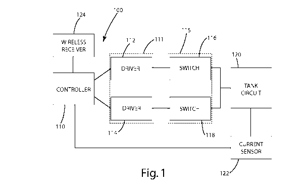
Fig. 1 is a block diagram of an inductive power supply.
Fig. 2 is a block diagram of a secondary circuit.
Figs. 3A and 3B together are a circuit diagram of an inductive power supply.
Fig. 4 is a circuit diagram of a secondary circuit.
Fig. 5 is a flowchart of a process to maintain resonance and adjust duty
cycle.
Fig. 6 is a flowchart of a process to adjust the operating frequency to
maintain
resonance.
Fig. 7 is an exemplary graph showing frequency versus power transfer
efficiency.
Fig. 8 is a timing diagram showing a varying duty cycle.
3
CA 02711489 2010-07-06
WO 2009/089253 PCT/US2009/030280
DESCRIPTION OF THE CURRENT EMBODIMENT
1. Overview
An inductive power supply or primary circuit in accordance with an
embodiment of the present invention is shown in Fig. 1, and generally
designated 100. The
primary circuit 100 includes a primary controller 110, a driver circuit 111
including a pair of
drivers 112, 114, a switching circuit 115 including a pair of switches 116,
118, a tank circuit
120 a primary sensor 122 and an optional wireless receiver 124. The primary
controller 110,
driver circuit 111 and the switching circuit 115 together generate an AC
signal at a selected
frequency and selected duty cycle that is applied to the tank circuit 120 to
create an inductive
field for transferring power wirelessly to a secondary circuit. A secondary
circuit in
accordance with an embodiment of the present invention is shown in Fig. 2, and
generally
designated 200. The secondary circuit 200 may include a secondary 210, a
rectifier 212, a
switch 214, a load 216, a current sensor 218 or voltage sensor 220, a
secondary controller
222, a signal resistor 224 for communicating using reflected impedance and an
optional
wireless transmitter 226.
In operation, an embodiment of the process for adjusting the duty cycle is
shown in Fig. 5, the initial operating frequency is set substantially at
resonant frequency 504
and the initial duty cycle is set at a relatively low value 506. The primary
controller
continuously adjusts the operating frequency 508 to maintain substantially
resonant
frequency and continuously determines if the amount of power being transferred
is too high
510. If too much power is being provided or temperatures are above a preset
threshold then
the duty cycle is decreased 514. If too little power is being provided then
the duty cycle is
increased 512. Various conditions may temporarily or permanently reduce or
halt the power
transfer.
4
CA 02711489 2010-07-06
WO 2009/089253 PCT/US2009/030280
II. Inductive Power Supply
The present invention is suitable for use with a wide variety of inductive
power supplies. As used herein, the term "inductive power supply" is intended
to broadly
include any inductive power supply capable of providing power wirelessly. The
present
invention is also suitable for use with "adaptive inductive power supplies."
As used herein,
the term "adaptive inductive power supply" is intended to broadly include any
inductive
power supply capable of providing power wirelessly at a plurality of different
frequencies.
For purposes of disclosure, the present invention is described in connection
with a particular
adaptive inductive power supply, shown in Figs. 3A and 3B and generally
designated 300.
The illustrated adaptive inductive power supply 300 is merely exemplary,
however, and the
present invention may be implemented with essentially any inductive power
supply that can
be modified to provide inductive power at varying duty cycles.
In the illustrated embodiment, the adaptive inductive power supply 300
generally includes a primary controller 310, a low voltage power supply 312,
memory 314, a
driver circuit 316, a switching circuit 318 a tank circuit 320, a current
sensor 322, a filter 324
and optionally a wireless receiver 326. In operation, the primary controller
310, driver circuit
316 and switching circuit 318 apply power to the tank circuit 320 to generate
a source of
electromagnetic inductive power at a selected frequency and a selected duty
cycle.
The primary controller 310 of the illustrated embodiment includes two
microcontrollers, one to control the frequency and one to control the duty
cycle. The
frequency microcontroller may be a microcontroller, such as a PIC24FJ32GA002,
or a more
general purpose microprocessor. The duty cycle microcontroller may be a
microcontroller,
such as a dsPIC30F2020, or a more general purpose microprocessor. In
alternative
embodiments, the primary controller 310 may be implemented using a single
microcomputer,
FPGA, analog or digital circuit. The driver circuit 316 may be discrete
components, as
CA 02711489 2010-07-06
WO 2009/089253 PCT/US2009/030280
shown in Fig. 3B, or they may be incorporated into the primary controller 310.
An oscillator
(not shown) may be included within the primary controller 310.
The primary circuit 300 may also include a low voltage power supply 312 for
supplying low voltage power to the primary controller 310, the driver circuit
as well as any
other components requiring low voltage power for operation. In the illustrated
embodiment
the low voltage power supply 312 provides scales the input voltage to 3.3
volts. In
alternative embodiments, a different voltage may be provided.
In the current embodiment, the various components of the primary circuit 310
collectively drive the tank circuit 320 at a frequency and duty cycle dictated
by the primary
controller 310. More specifically, the primary controller 310 controls the
timing of the driver
circuit 316 and switching circuit 318. The timing refers to both the frequency
and duty cycle
of the signal being generated. Frequency as it is being used here refers to
the number of
repetitions per unit time of a complete waveform. Duty cycle refers to the
proportion of time
during which the waveform is high compared to the total amount of time for a
complete
waveform. Thus, a square wave as shown in Fig. 8, may be described by its
frequency and its
duty cycle. Further, the duty cycle may be adjusted while maintaining the same
frequency
and the frequency may be adjusted while maintaining the same duty cycle. The
driver circuit
316 of the illustrated embodiment includes two separate drivers and may
include additional
circuit components to boost and filter the signal. For example, in the current
embodiment,
the signal is boosted to 20 volts, without effecting the timing of the signal.
The switching circuit 318 includes two switches. In the current embodiment,
the switches are implemented as MOS field effect transistors. In alternative
embodiments,
other circuit components may be used to implement the switching circuit.
Additionally,
depending on power requirements MOSFETs with different characteristics may be
implemented during manufacture. In some embodiments, multiple sets of switches
may be
6
CA 02711489 2010-07-06
WO 2009/089253 PCT/US2009/030280
provided on the circuit board, allowing one set of switches to be soldered at
the time of
manufacture based on the particular power requirements of that application.
In one embodiment, the switching circuit 115 includes two separate switches
116, 118 that are switched on at the same frequency, but out of phase with
each other. Fig. 8
illustrates the timing for one embodiment of such a switching circuit. In Fig.
8, both switches
have the same duty cycle, but are shifted in time from each other by half of
the period of the
switching waveform. In alternative embodiments, each switch may have a
different duty
cycle and they the switches may be shifted in time a different amount from
each other. That
is, half period separation and similar duty cycle are desirable, but
unnecessary, for the
switches because it may result in increased power transfer efficiency from the
inductive
power supply to the remote device.
The tank circuit 320 generally includes the primary and a capacitor. The
primary of the current embodiment is an air-core coil inductor. A cored
inductor can also be
used if the proper considerations are made for spatial freedom, monitoring
overall power, and
feedback. The capacitance of the capacitor may be selected to balance the
impedance of the
primary coil at anticipated operating parameters. In the current embodiment,
although three
tank capacitors are shown, all three capacitors need not necessarily be
soldered into the
circuit at the time of manufacture. An inductive power supply may be
fabricated which at the
time of soldering can have an appropriate capacitance value selected by
soldering or
switching different capacitors into the circuit. The tank circuit 320 may be
either a series
resonant tank circuit (as shown in Fig. 3B) or a parallel resonant tank
circuit (not shown).
The present invention may be incorporated into the adaptive inductive power
supply shown
in U.S. Patent 6,825,620, which is incorporated herein by reference. As
another example, the
present invention may be incorporated into the adaptive inductive power supply
shown in
U.S. Patent Application Publication US2004/130916A1 to Baarman, which is
entitled
7
CA 02711489 2010-07-06
WO 2009/089253 PCT/US2009/030280
"Adapted Inductive Power Supply" and was published on July 8, 2004 (U.S.
Serial No.
10/689,499, filed on October 20, 2003), which is also incorporated herein by
reference.
Further, it may be desirable to use the present invention in connection with
an adaptive
inductive power supply capable of establishing wireless communications with
the remote
device, such as the adaptive inductive power supply shown in U.S. Patent
Application
Publication US 2004/130915A1 to Baarman, which is entitled "Adapted Inductive
Power
Supply with Communication" and was published on July 8, 2004 (U.S. Serial No.
10/689,148, filed on October 20, 2003), which is incorporated herein by
reference. Further
yet, it may be desirable to use the present invention with a printed circuit
board coil, such as a
printed circuit board coil incorporating the invention principles of U.S.
Serial No.
60/975,953, which is entitled "Printed Circuit Board Coil" and filed on
September 28, 2007
by Baarman et al, and which is incorporated herein by reference in its
entirety. In other
alternative embodiments, the inductor may be implemented as a multi-tap
inductor and/or the
capacitors may be implemented as a switched capacitor bank that may be used to
dynamically, before or during use, alter the resonance of the primary circuit,
for example, as
described in U.S. Patent 7,212,414, which is entitled "Adaptive Inductive
Power Supply" and
issued May 1, 2007, to Baarman, which is herein incorporated by reference.
In certain modes of operation, the primary controller 310 may establish the
operating frequency as a function of input from the current sensor 322. The
controller 310, in
turn, operates the driver circuit 318 at the frequency established by the
primary controller
310. The driver circuit 316 provides the signals necessary to operate the
switching circuit
318. As a result, the switching circuit 318 provides AC (alternating current)
power to the
tank circuit 320 from a source of DC (direct current) power. In an alternative
embodiment,
the operating frequency is established from a separate communication link,
such as the
wireless receiver 326, implemented in the current embodiment as an IR
receiver.
8
CA 02711489 2010-07-06
WO 2009/089253 PCT/US2009/030280
The primary controller 310 may also establish the duty cycle as a function of
input from the current sensor 322. Planned shunting of the signal resistor on
the secondary,
which will be described in more detail below, may be used to provide
information to the
primary using reflected impedance detected with the current sensor 322.
Alternatively, the
duty cycle may be established using a separate communication link, such as the
wireless
receiver 326, implemented in the current embodiment as an IR receiver. This
could also be
near field or other RF communication channels.
In the illustrated embodiment, the current sensor 322 is a current transformer
having a primary coil connected to the tank circuit and a secondary coil
connected to the
primary controller 310. In the current embodiment, the current sensor 322
includes circuitry
to adjust the gain of the output of the current sensor to accommodate the
ranges accepted by
the primary controller 310. Further, the amount of gain may be adjusted by the
primary
controller 310 by applying a signal to the switch. The inductive power supply
300 may
include conditioning circuitry 324 for conditioning the current transformer
output before it is
supplied to the primary controller 310. In the current embodiment, the
conditioning circuitry
324 is a 5K Hz 2-pole filter. Although the illustrated embodiment includes a
current
transformer for sensing the reflected impedance of the secondary or remote
device, the
inductive power supply 300 may include essentially any alternative type of
sensor capable of
providing information regarding reflected impedance from the secondary 400.
Further,
although the current sensor 322 of the illustrated embodiment is connected
directly to the
tank circuit, the current sensor (or other reflected impedance sensor) can be
located in
essentially any location where it is capable of providing readings indicative
of the reflected
impedance.
In the illustrated embodiment, the inductive power supply 300 further includes
a memory 314 capable of storing information relating to the operating
parameters of a
9
CA 02711489 2010-07-06
WO 2009/089253 PCT/US2009/030280
plurality of secondaries 400. The stored information may be used to permit the
inductive
power supply 300 to more efficiently power the secondary 400 and more readily
recognize
fault conditions. In some applications, the inductive power supply 300 may be
intended for
use with a specific set of secondaries 400. In these applications, the memory
314 includes the
unique resonant frequency (or pattern of frequencies) for each secondary 400,
along with the
desired collection of associated information, such as maximum and minimum
operating
frequencies, current usage and minimum and maximum duty cycle. The memory 314
may,
however, include essentially any information that may be useful to the
inductive power
supply 300 in operating the secondary 400. For example, in applications where
it is desirable
to establish wireless communications with the secondary 400, the memory 314
may include
information regarding the wireless communication protocol of the remote device
400.
III. Secondary Circuit
The present invention is intended for use with a wide variety of remote
devices or secondaries of varying designs and constructions. It is anticipated
that these
various remote devices will require power at varying frequency and will have
different power
requirements.
For purposes of disclosure, one embodiment of a secondary circuit 400 is
shown in Fig. 4. In the embodiment of Fig. 4, the secondary circuit 400
generally includes a
secondary 410 for receiving power from the inductive power supply 300, a
rectifier 414 (or
other components for converting AC power to DC), a low voltage power supply
412 that
scales the received power to operate the secondary controller 428,
conditioning circuitry 416,
426 to remove ripple in the signal, current sensor 418, voltage sensor 422,
switch 420, load
424, secondary controller 428, a signal resistor 432 and an optional wireless
transmitter 430.
In operation, the rectifier 414 converts the AC power generated in the
secondary 410 to DC
power, which is typically needed to power the load. Alternatively, multiple
secondary coils
CA 02711489 2010-07-06
WO 2009/089253 PCT/US2009/030280
receiving power on different phases can be used to reduce the ripple voltage.
This is
referenced in Application 60/976,137, entitled Multiphase Inductive Power
Supply System to
Baarman et al, which is herein incorporated by reference. Multiple primary
coils may be
desired to transmit power on different phases in such an embodiment. In one
embodiment,
the load is a charging circuit (not shown) for a battery. Charging circuits
are well-known and
are widely used with a variety of rechargeable electronic devices. If desired,
the charging
circuit may be configured to both charge a battery (not shown) and/or power
the load 424. In
alternative embodiments the rectifier may be unnecessary and AC power may be
conditioned
to be used to power the load.
The current sensor 418 detects the amount of current in the received power
and provides that information to the secondary controller 428. The voltage
sensor 422
detects the amount of voltage in the received power and provides that
information to the
secondary controller 428. Although the illustrated embodiment includes both a
voltage
sensor 422 and a current sensor 418, only one is necessary. By sensing the
voltage and/or
current in the secondary circuit and knowing the voltage and/or current
provided by the
primary circuit, the primary controller can calculate the power transfer
efficiency. By
sweeping a range of operating frequencies, noting the power transfer
efficiency at each
frequency, the operating frequency closest to resonance can be determined - it
corresponds
with the operating frequency that yields the best power transfer efficiency.
In addition, the
voltage and current sensors 418, 422 can be used in conjunction with a
protection algorithm
in the secondary controller 428 to disconnect the load 424 if a fault
condition is detected.
This concept is described in more detail in U.S. Patent Application No.
11/855,710 entitled
System and Method for Inductively Charging a Battery to Baarman et al, which
was
previously incorporated by reference.
The secondary controller 428 may be essentially any type of microcontroller.
11
CA 02711489 2010-07-06
WO 2009/089253 PCT/US2009/030280
In the illustrated embodiment, the secondary controller 428 is an ATTINY24V-
10MU
microcontroller. The secondary controller 428 generally includes an analog to
digital
converter, and is programmed to process the voltage and/or current readings
and transmit
them to the primary controller 310 of the inductive power supply 300. The
microprocessor
may also include other code unrelated to the frequency or duty cycle control
processes.
Communication of the sensed voltage and/or current in the secondary may be
transmitted to the primary controller 310 in a variety of ways. In the
illustrated embodiment,
the information may be transmitted using the signal resistor 432 or the
wireless transmitter
430.
In one embodiment, signal resistor 432 may be used to send information to the
primary controller 310. The use of a signal resistor 432 to provide
communication from the
secondary to the primary was discussed in U.S. Patent Application No.
11/855,710 entitled
System and Method for Inductively Charging a Battery to Baarman et al, which
is herein
incorporated by reference. The signal resistor 432, when shunted, sends a
communication
signal that signifies an over-current or over-voltage state. When the resistor
is shunted, the
peak detector on the primary circuit is able to sense the over-voltage/over-
current condition
and act accordingly. The signal resistor 432 of the present invention may be
shunted
systematically to communicate additional data to the primary controller 310.
For example, a
stream of data could represent the sensed current and/or sensed voltage.
Alternatively, the
signal resistor could be used solely in the previously described way as an
over-voltage/over-
current transmitter or it could be removed entirely.
Use of a wireless transmitter or transceiver was previously described in U.S.
Patent Application Publication US 2004/130915A1 to Baarman, which is entitled
"Adapted
Inductive Power Supply with Communication" that was previously incorporated by
reference. Specifically, the use of WIFI, infrared, blue tooth, cellular or
RFID were
12
CA 02711489 2010-07-06
WO 2009/089253 PCT/US2009/030280
previously discussed as ways to wirelessly transmit data from a remote device
to an inductive
power supply. Further, communication using the induction coils and a power
line
communication protocol was discussed. Any of these methods of transmitting
data could be
implemented in the present invention in order to transfer the desired data
from the secondary
to the primary.
IV. Operation
General operation of the primary circuit 100 and secondary circuit 200 is
described in connection with Fig. 5.
In this embodiment, the primary circuit determines and sets the initial
operating frequency 504. Typically, the goal of setting the initial operating
frequency is to
set it as close to the resonant frequency as possible, which varies depending
on many
different factors including, among other things, the orientation and distance
between the
primary circuit and secondary circuit. In the current embodiment, a simple
frequency sweep
is used to determine where to set the initial operation frequency.
Specifically, in this
embodiment, the range of valid frequencies is swept and the power transfer
efficiency at each
frequency is noted. The step between frequencies may vary, but in the current
embodiment,
the frequency is swept between 70k Hz and 250k Hz at steps of 100 Hz. Once the
entire
range of frequencies has been swept, the operating frequency that yielded the
highest power
transfer efficiency is selected as the initial operating frequency. The
operating frequency that
yielded the highest power transfer efficiency indicates that it is the closest
frequency to
resonance. Further steps at a finer frequency resolution can facilitate even
further tuning.
Other methods for determining the initial operating frequency may be used in
alternative
embodiments. For example, an initial operating frequency may be selected based
on known
primary and secondary component. Further, modifications to the sweeping
process may
include dynamic step adjustment proportional to the power transfer efficiency.
In yet another
13
CA 02711489 2010-07-06
WO 2009/089253 PCT/US2009/030280
alternative embodiment, the sweep may be performed dynamically so that only
the power
transfer efficiency value for the current frequency and the frequency with the
highest power
transfer efficiency are stored. As the sweep progresses, each value is checked
against the
highest stored value and replaces it only if it is higher.
In the embodiment described in Fig. 5, the primary circuit sets the initial
duty
cycle 506. The duty cycle corresponds with the amount of power transferred
with each cycle.
The higher the duty cycle, the more power transferred per cycle. In the
current embodiment,
the initial duty cycle is set at 20%, which is considered low enough to not
risk over-powering
the remote device, but is high enough such that enough power is transferred to
power the
secondary circuitry. In alternative embodiments a different initial duty cycle
may be set
based on the application or any number of other factors.
The adjust operating frequency step 508 is a multi-step process which ensures
that the operating frequency is being maintained substantially at resonance.
Fig. 6 describes
one embodiment of this process in more detail. In the described embodiment,
the operating
frequency is increased by a pre-selected amount, referred to as a step up. The
adjustment is
allowed to propagate through the system and the power efficiency is checked
604. If the
power efficiency increased then the system was not substantially at resonance
and the
operating frequency is stepped up again. This process continues until the
power efficiency
either decreases or stays the same. Once that occurs, the operating frequency
is stepped
down 608. The power efficiency is checked 608. If the power efficiency
increases then the
operating frequency is stepped down again, until the power efficiency stays
the same or
decreases. The final step is to step up the operating frequency 610 to get
back to the
operating frequency with the peak power efficiency. This is merely one
embodiment of a
process to maintain the operating frequency substantially at resonance. Any
other process
could be used to maintain the operating frequency substantially at resonance.
14
CA 02711489 2010-07-06
WO 2009/089253 PCT/US2009/030280
One reason that the operating frequency is stepped up and stepped down can
be explained by looking at an exemplary graph of operating frequency vs. power
efficiency,
shown in Figure 7. As can be seen, there are several peaks of power efficiency
over the range
of operating frequencies shown. The initial sweep of frequencies sets the
operating
frequency to the resonant frequency, i.e. the highest peak on Figure 7. Each
time the
adjustment comes, although the operating frequency has not changed, the power
efficiency
values may have changed as a result in any number of factors, most notably
movement of the
secondary. Typically, the change in the graph is merely a slight shift,
meaning that the
optimum operating frequency may be a few steps in either direction. This is
why the current
embodiment steps up and steps down. If the first step up leads to a decrease
in power
efficiency transfer, the process immediately steps down until. If stepping
down also leads to
a decrease in power efficiency transfer then it is evident that no adjustment
is necessary and
the operating frequency was already at resonant frequency. In an alternative
embodiment an
analog circuit could be used to directly determine how far off resonance the
system is,
causing the controller to react directly to the proper frequency. A phase
comparator is one
such circuit.
In the current embodiment, the operating frequency is adjusted with each
iteration, however, in alternative embodiments, the operating frequency may be
adjusted less
frequently or only when an event triggers that it should be adjusted. For
example, if a motion
detector on the secondary indicates movement or a change in orientation of the
secondary.
Or, for example, if there is a sharp decrease or increase in the amount of
power provided to
the secondary.
The next step is to determine if the amount of power being received by the
secondary is too high 510. If the amount of power being received is too high
then the duty
cycle of the power being transferred is reduced 514. If the amount of power
being received is
CA 02711489 2010-07-06
WO 2009/089253 PCT/US2009/030280
not too high then the duty cycle of the power being transferred is increased
512. In the
current embodiment, the duty cycle should not exceed approximately 49% in
order to reduce
the risk of causing a short circuit. In the current embodiment, after the duty
cycle is
adjusted, up or down, the operating frequency is re-adjusted 508. As explained
above, duty
cycle refers to the "switch on time" or the proportion of time during which
the waveform is
high compared to the total amount of time for a complete waveform. An
exemplary graph
illustrating a signal with a varying duty cycle is shown in Fig. 8. The graph
depicts a graph
of time vs. current. The solid line represents the waveform generated by the
primary circuit
with the current duty cycle. The dashed line represents what a waveform would
look like
with an increased duty cycle. The dash-dotted line represents what a waveform
would look
like with a decreased duty cycle. Note that because the duty cycle is being
increased
symmetrically and decreased symmetrically, the frequency of the waveform does
not change
with the adjustment in duty cycle. It is worth noting that in some
embodiments, during
operation, the frequency may not be adjusted, while duty cycle adjustments
continue to take
place.
Duty cycle may be stepped up or down by a pre-selected amount. In the
current embodiment, the step up and step down amounts are static and equal.
However, in
alternative embodiments, the step amounts may be dynamic and different. For
example, in
battery charging applications it may be beneficial to decrease duty cycle in
large steps and
increase duty cycle in small steps. Various batteries require different
charging algorithms
and the duty cycle control may be used to provide the correct battery charging
profile. In
another example, the duty cycle may be stepped up or down proportional to the
amount of
power demanded by the secondary. The amount of power demanded by the secondary
can be
determined by reading the current and/or voltage sensor. Where there is a
small change in
the readings, a small change in duty cycle may be implemented and where there
is a large
16
CA 02711489 2010-07-06
WO 2009/089253 PCT/US2009/030280
change in the readings, a large change in duty cycle may be implemented.
In one embodiment, there are built-in delays between the changes in operating
frequency and changes in duty cycle. These delays can account for any phase
issues that may
arise because of the speed at which the operating frequency or duty cycle is
being changed.
This process continues as desired or until the power supply is turned off, the
secondary is removed, or in the case of charging a battery, when the battery
is fully charged.
The primary circuit may adjust the duty cycle depending on the demands of
the secondary. For example, in one embodiment, one goal may be to maintain a
certain
amount of voltage or current in the secondary. Using feedback from the
secondary, such as
the sensed voltage and/or current, the operating frequency may be adjusted to
ensure
optimum power transfer efficiency by ensuring operation at substantially
resonant frequency
and the duty cycle may be adjusted to provide additional or less power to meet
the desired
goal.
The above description is that of the current embodiment of the invention.
Various alterations and changes can be made without departing from the spirit
and broader
aspects of the invention.
17