Note: Descriptions are shown in the official language in which they were submitted.
CA 02712148 2010-07-14
DESCRIPTION
METHOD FOR PRODUCING A LAMINATED BODY HAVING Al-BASED GROUP-III
NITRIDE SINGLE CRYSTAL LAYER, LAMINATED BODY PRODUCED BY THE
METHOD, METHOD FOR PRODUCING Al-BASED GROUP-III NITRIDE SINGLE
CRYSTAL SUBSTRATE EMPLOYING THE LAMINATED BODY, AND ALUMINUM
NITRIDE SINGLE CRYSTAL SUBSTRATE
Technical Field
[0001] The present invention relates to a method for
producing a substrate comprising a single crystal of an Al-based
group-III nitride such as aluminum nitride.
Background Art
[0002] An aluminum nitride (A1N) has a relatively large
bandgap, i.e. 6.2 eV, and it is a direct transition type
semiconductor, so that aluminum nitride is expected to be used
as a material for ultraviolet light emitting device, along with
a mixed crystal of gallium nitride (GaN) and indium nitride (InN)
as group-III nitrides where A1N belongs to, particularly a mixed
crystal having 50 atom % or more Al in the Group-III elements
(hereinafter, refer to as "Al-based group-III nitride single
crystal".).
[0003] To form a semiconductor device such as a ultraviolet
light emitting device, it is necessary to form a laminate
structure including e.g. clad layer and active layer between an
n-type semiconductor layer electrically connected to an
n-electrode and a p-type semiconductor layer electrically
1
CA 02712148 2010-07-14
connected to a p-electrode; in view of luminous efficiency, it
is important that all layers have high crystallinity, namely,
have less dislocation and less point defects. The laminate
structure is formed on a single crystal substrate having a
mechanical strength enough to beself -supporting or f ree-standing
(hereinafter, it may be referred to as "self-supporting
substrate".). The self-supporting substrate for forming the
laminate structure is required to have small difference in lattice
constant and small difference in coefficient of thermal expansion
with aluminum gallium indium nitride (AlGaInN) which forms the
laminate structure; moreover, self-supporting substrate is
required to have high thermal conductivity in view of preventing
deterioration of the devices. Therefore, to produce a
semiconductor device containing aluminum nitride, it is
advantageous to form the above layer structure on the Al-based
group-III nitride single crystal substrate.
[0004] So far, the Al-based group-III nitride single crystal
self-supporting substrate has not been commercially available.
So, there have been attempts to obtain an Al-based group-III
nitride single crystal substrate by method in which a thick film
made of Al-based group-III nitride single crystal is formed on
a different type of single crystal substrate such as sapphire
substrate (hereinafter, a substrate used for forming single
crystal thereon may be referred to as "base substrate". ) by vapor
phase epitaxy method; and then, the formed single crystal
substrate is separated from the base substrate. Examples of
vapor phase epitaxy method include: hydride vapor phase epitaxy
(HVPE) method, molecular beam epitaxy (MBE) method, and
2
CA 02712148 2010-07-14
metalorganic vapor phase epitaxy (MOVPE) method. In addition,
sublimation-recrystallization method and other epitaxies
through liquid phase may also be used. Among them, HVPE method
is not suitable for forming crystal lamination structure for
semiconductor light emitting device as it is difficult to control
the film thickness accurately compared with MOVPE method and MBE
method; however, HVPE method can provide a single crystal with
good crystallinity at high growth rate, therefore HVPE method
is frequently used for vapor phase epitaxy aiming at forming a
single crystal thick film.
[0005] Nevertheless, when forming a group-III nitride
single crystal, such as GaN, including Al-based group-III nitride
single crystal by the vapor phase epitaxy method, it is difficult
to inhibit dislocation generation from interface by
lattice-mismatch between a substrate and a growing group-III
nitride. In addition, since the crystal grows at a high
temperature around 1000 C, when a thick film is formed, due to
the difference in coefficient of thermal expansion of the film
from that of the substrate, warpage occurs after the growth;
thereby, dislocation increases by stress and crackings occur,
which are problematic. Even when a self-supporting substrate can
be obtained without breakage and cracks, inhibiting warpage is
extremely difficult; therefore, to obtain an self-supporting
substrate, a treatment for making the surface flat by reducing
warpage has been necessary.
[0006] With respect to the group-III nitride single crystal
self-supporting substrate such as GaN substrate, the following
method is proposed to solve the above problems. That is, Patent
3
CA 02712148 2010-07-14
document 1 proposes a method comprising the steps of: growing
a group-III nitride single crystal such as GaN on an
acid/alkaline-soluble single crystal substrate such as GaAs
substrate; growing a polycrystal group-III nitride; removing the
single crystal substrate using acid or alkaline solution; and
then growing a single crystal group-III nitride layer on the
remaining group-III nitride single crystal formed in the first
step. In the examples of Patent document 1, in accordance with
the method, a 200 nm thick GaAs buffer layer and a 20 nm thick
GaN buffer layer were formed on a GaAs (111) substrate where a
SiO2 layer is formed on the back side as a protection layer, then,
a 2 pm thick GaN layer with favorable crystallinity and a 100
pm thick GaN layer wherein less significance is placed on
crystallinity (the surface of which is polycrystal) were grown
sequentially, the GaAs was dissolved and removed to obtain a GaN
substrate, and finally a 15 pm thick GaN single crystal layer
was grown on the surface of the obtained substrate to which the
GaAs substrate has abutted; the obtained GaN single crystal layer
does not have cracks and does show dislocation number of around
105/cm2.
[0007]
Patent Document 1: Japanese Patent No. 3350855
Disclosure of the Invention
Problems to be solved by the Invention
[0008] The present inventors initially thought that they
could produce a favorable self-supporting substrate by adopting
a similar method as proposed in Patent document 1 even when
4
CA 02712148 2010-07-14
producing an Al-based group-III nitride single crystal
self-supporting substrate such asA1N substrate and they actually
tried. However, when producing a laminated body having a similar
layer construction as that of the examples and removing the base
substrate by dissolution, it is difficult to inhibit breakage
and cracking; thus, even when an self-supporting substrate having
no breakage and cracks can be obtained, warpage cannot be
sufficiently inhibited.
[0009] Accordingly, an object of the present invention is
to provide "a substrate of which surface is formed by an Al-based
group-III nitride single crystal and which has no cracks and
warpage" to be suitably used as a base substrate for producing
an Al-based group-III nitride single crystal self-supporting
substrate and a method for efficiently producing a high-quality
Al-based group-III nitride single crystal self-supporting
substrate.
Means for Solving the Problems
[0010] The inventors considered that the reason why the
effect observed in the case of GaN when employing the method of
Patent document 1 could not be obtained in the case of Al-based
group-III nitride was that Al-based group-III nitride contained
high ratio of Al, so that it was hard and poor in elasticity and
the temperature for vapor phase epitaxy was high, compared with
GaN. In a case of forming a thick group-III nitride single crystal
film using a base substrate made of e. g. sapphire, SiC, and silicon,
due to the difference in lattice constant and difference in
coefficient of thermal expansion between the base substrate and
CA 02712148 2010-07-14
the group-III nitride single crystal, stress occurs to the
group-III nitride single crystal (hereinafter, it maybe referred
to as "lattice-mismatch strain".). If a relatively resilient
material such as GaN is used, cracking and breakage hardly occur
under occurrence of lattice-mismatch strain; however, if a harder
material such as Al-based group-III nitride is used, cracking
and breakage tend to occur. Moreover, if the temperature of
crystal growth is high, for example at 1100 C, lattice-mismatch
strain increases because of shrinkage during cooling step after
film forming; thereby the problems becomes more obvious. Hence,
the above result was obtained.
[0011] Based on the above assumption, the inventors thought
that if the Al-based group-III nitride single crystal layer to
be formed on the base substrate becomes thinner, cracking and
breakage by the lattice-mismatch strain can be inhibited and
degree of warpage can be reduced; so, they examined influences
of the thickness of the Al-based group-III nitride single crystal
layer and the thickness of the Al-based group-III nitride
polycrystal layer to be formed on the base substrate as well as
the thickness ratio of the both layers on the properties of the
substrate (remaining part after removing base substrate) As a
result, the inventors discovered that: when the Al-based
group-III nitride single crystal layer to be formed on the base
substrate is made thicker and is cooled without forming an
Al-based group-III nitride polycrystal layer thereon, cracking,
breakage, and warpage tends to occur; if an Al-based group-III
nitride polycrystal layer is formed on the Al-based group-III
nitride single crystal layer and then cooled, even when the single
6
CA 02712148 2010-07-14
crystal layer is made thicker, cracking, breakage, and warpage
are reduced, in other words, the polycrystal layer not only
functions to increase thickness but also functions to slightly
reduce lattice-mismatch strain. Hence, the inventors completed
the present invention.
[0012] The first aspect of the present invention is a method
for producing a laminated body having a laminate structure
comprising: an Al-based group-III nitride single crystal layer
having a composition represented by All-(x+y+Z)GaxInyBZN (wherein,
x, y, and z are independently a rational number of 0 or more and
below 0 . 5 ; the sum of x, y, and z is below 0. 5.) ; and a non-single
crystal layer made of a material for forming the Al-based
group-III nitride single crystal layer or a material containing
the material for forming the Al-based group-III nitride single
crystal layer as a main component, wherein a main surface of the
Al-based group-III nitride single crystal layer is exposed, the
method comprising the steps of:
(1) preparing a base substrate having a surface formed of
a single crystal of which material is different from the material
constituting the Al-based group-III nitride single crystal layer
to be formed;
(2) forming the Al-based group-III nitride single crystal
layer having a thickness of 10 nm to 1.5 }lm on the single crystal
surface of the prepared base substrate;
(3) producing a laminated substrate where the Al-based
group-III nitride single crystal layer and the non-single crystal
layer are formed on the base substrate by forming on the Al-based
group-III nitride single crystal layer a non-single crystal layer
7
CA 02712148 2010-07-14
being 100 times or more thicker than the Al-based group-III
nitride single crystal layer without breaking the
previously-obtained Al-based group-III nitride single crystal
layer; and
(4) removing the base substrate from the laminated
substrate obtained in the previous step.
[0013] According to the method, it is possible to
efficiently produce a laminated body, which is the
below-described second aspect of the invention, suitably used
as an Al-based group-III nitride single crystal self-supporting
substrate.
[0014] In the method according to the first aspect of the
invention, the non-single crystal layer, in the step (3), is
preferably a layer formed of: polycrystal, amorphous, or a mixture
thereof of a material for forming the Al-based group-III nitride
single crystal layer or of a material containing the material
for forming the Al-based group-III nitride single crystal layer
as a main component. If the non-single crystal layer is such a
layer, stress attributed to the difference in lattice constant
of the base substrate with the Al-based group-III nitride single
crystal can be slightly reduced. Therefore, by making the
Al-based group-III nitride single crystal layer thinner, for
example 1.5 pm or less, and making the non-single crystal layer
be 100 times or more thicker than the single crystal layer, it
becomes possible to carry out cooling after film forming without
causing any large warpage and cracking in the Al-based group-III
nitride single crystal. The reason for obtaining such an effect
is assumed that when the non-single crystal layer is a polycrystal
8
CA 02712148 2010-07-14
layer, there exists an interface of crystal particles, i.e. grain
boundary; thereby, stress (namely, lattice-mismatch strain)
caused by difference in lattice constant or coefficient of thermal
expansion of Al-based group-III nitride single crystal layer with
the base substrate is reduced. When the non-single crystal layer
is an amorphous layer, it is assumed that the amorphous layer
is made of extremely fine crystals of the Al-based group-III
nitride, so that it is a state where no long-period structure
of atomic arrangement is formed; thereby, the stress is reduced
along the grain boundary of the above extremely fine crystal.
[0015] The non-single crystal layer needs to be formed on
a previously formed Al-based group-III nitride single crystal
layer without breaking the Al-based group-III nitride single
crystal layer. The suitable method for forming the non-single
crystal layer satisfying these conditions is a method where both
formation of the Al-based group-III nitride single crystal layer
in the step (2) and formation of the non-single crystal layer
in the step (3) are carried out by vapor phase epitaxy method,
and the formation of the Al-based group-III nitride single crystal
layer and the formation of the non-single crystal layer are
successively performed by using a same apparatus. If the method
is adopted, adhesiveness between the Al-based group-III nitride
single crystal layer and the non-single crystal layer can be
higher. It should be noted that it is necessary to meet the above
conditions when forming the non-single crystal layer, so that
the methods which does not meet the conditions, for example, a
method comprising the step of forming a polycrystal body by
sintering a ceramic powder cannot be adopted.
9
CA 02712148 2010-07-14
[0016] The second aspect of the present invention is a
laminated body having a laminate structure comprising: an
Al-based group-III nitride single crystal layer having a
composition represented by All- (X+Y+Z)GaXInYBZN (wherein, x, y, and
z are independently a rational number of 0 or more and below 0.5;
the sum of x, y, and z is below 0. 5.) and having a thickness of
nm to 1.5 pm; and a non-single crystal layer consisting of
a non-sintered material which is made of a material for forming
the Al-based group-III nitride single crystal layer or a
non-sintered material containing the material for forming the
Al-based group-III nitride single crystal layer as a main
component and which is 100 times or more thicker than that of
the Al-based group-III nitride single crystal layer, a surface
of the Al-based group-III nitride single crystal layer being
exposed. The laminated body can be suitably used as a substrate
for producing an Al-based group-III nitride single crystal
self-supporting substrate. Due to the above-mentioned reason,
the non-single crystal layer in the laminated body is constituted
by a non-sintered material (in the invention, the term
"non-sintered material" means a material other than a sintered
body made by sintering a powder material.).
[0017] The third aspect of the present invention is a method
for producing the Al-based group-III nitride single crystal,
comprising the step of growing epitaxially an Al-based group-III
nitride single crystal (it may be referred to as a "second Al-based
group-III nitride single crystal".) having the same composition
as or the similar composition to the Al-based group-III nitride
constituting the Al-based group-III nitride single crystal layer,
CA 02712148 2010-07-14
on the Al-based group-III nitride single crystal layer of the
laminated body according to the second aspect of the invention.
[0018] The fourth aspect of the present invention is a method
for producing the Al-based group-III nitride single crystal
substrate, comprising the step of forming a second Al-based
group-III nitride single crystal layer on the Al-based group-III
nitride single crystal layer of the laminated body according to
the second aspect of the invention by growing epitaxially an
Al-based group-III nitride single crystal (i.e. the second
Al-based group-III nitride single crystal) having the same
composition as or the similar composition to the Al-based
group-III nitride constituting the Al-based group-III nitride
single crystal layer.
[0019] As described above, the first to fourth aspects of
the invention are related to each other; in the fourth aspect
of the invention, the laminated body according to the second
aspect of the invention which is produced by the first aspect
of the invention is used as a base substrate, then, by employing
the method for producing the Al-based group-III nitride single
crystal according to the third aspect, an Al-based group-III
nitride single crystal substrate is produced. The relations are
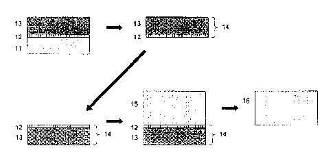
schematically shown in Fig. 1.
[0020] As shown in Fig. 1, the first method of the invention
comprises: the steps of (1) to (3) for forming a laminated
substrate where an Al-based group-III nitride single crystal
layer 12 and a non-single crystal layer 13 are laminated, in the
order mentioned, on a base substrate; and the step (4) for
separating the base substrate 11 from the laminated substrate,
11
CA 02712148 2010-07-14
to produce the laminated body 14 according to the second aspect
of the invention where the Al-based group-III nitride single
crystal layer 12 and non-single crystal layer 13 are adhered.
Later, in the third aspect of the invention, the laminated body
14 is used as a base substrate of which the exposed surface of
Al-based group-III nitride single crystal layer 12 is the crystal
growing surface, to grow epitaxially the second Al-based
group-III nitride single crystal. Finally, in the fourth aspect
of the invention, a second Al-based group-III nitride single
crystal layer 15 is obtained by growing the second Al-based
group-III nitride single crystal in a layer form, and then at
least a part of the Al-based group-III nitride single crystal
layer 15 is separated to obtain an Al-based group-III nitride
single crystal substrate 16 usable for an self-supporting
substrate.
[0021] The present inventors produced the A1N single crystal
substrates usable as an self-supporting substrate in the above
manner and evaluated the substrates. Then, the inventors
discovered that when growing the A1N single crystal in a
temperature range of 1400-1900 C, concentration of impurity such
as oxygen and silicon contained in the obtained A1N single crystal
substrate becomes extremely low, thereby extremely high purity
can be attained, which has never been attained by the A1N single
crystal substrate produced by the conventional methods.
That is, the invention also provides, as the fifth aspect
of the invention, an aluminum nitride single crystal substrate
having an oxygen concentration of 2.5 x 10¹⁷ atom/cm3 or less and
a ratio (A/B) of a spectral intensity (A) at an emission wavelength
12
CA 02712148 2010-07-14
of 210 nm to a spectral intensity (B) at an emission wavelength
of 360 nm under photoluminescence measurement at 23 C being 0.50
or more.
[0022] In general, when forming the AlN single crystal layer
on a base substrate by the vapor phase epitaxy method, it is
inevitable that atoms contained in the material constituting the
base substrate are taken in the AlN single crystal layer as an
impurity by thermal diffusion. Moreover, when employing an
apparatus using materials being the source of oxygen or silicon,
such as quartz, as a vapor phase epitaxy apparatus, these elements
contaminate the crystal as impurities from the atmosphere during
the growth of the crystal. As a result, the AlN single crystal
substrate obtained by growing the AlN single crystal on a sapphire
substrate or a silicon substrate by HVEPE method using quartz-made
apparatus usually contains oxygen of about 1018-19 atom/cm3 and
silicon of about 1018 atom/cm3. Further, even when producing the
A1N single crystal substrate by sublimation method, the lower
limit of the oxygen concentration is about 3 x 10¹⁷ atom/cm3 (see
Journal of Crystal Growth (2008), doi: 10.1016/j.jcrysgro. 2008.
06032).
[0023] On the other hand, with respect to the aluminum
nitride single crystal substrate according to the fifth aspect
of the invention, the laminated body according to the second
aspect of the invention is used as the base substrate and the
invention succeeds in inhibiting contamination by impurities such
as oxygen and silicon by performing vapor phase epitaxy of the
AlN single crystal within a particular temperature range. Below
is the inventors' assumption regarding the reasons why these
13
CA 02712148 2010-07-14
effects can be obtained. That is, the concentration of the
impurities seems to significantly decline, because: (i) the
concentration of atoms as the impurities contained in the base
substrate to be used is originally low, (ii) the crystal growing
surface of the base substrate is an "N-polar plane of the AlN
single crystal" where AlN does not grow by the conventional vapor
phase epitaxy method, so that polarity reversion is caused at
the initial phase of AlN growth on the N-polar plane and a kind
of barrier layer is formed, whereby diffusion of the atoms as
impurities from the base substrate is inhibited; and (iii)
contamination by impurities from the atmosphere is inhibited by
growing crystal in a high temperature range of 1400-1900 C.
Effects of the Invention
[0024] According to the first aspect of the invention, the
laminated body according to the second aspect of the invention
can be efficiently produced. In addition, by the method, by
controlling the shape and size of the base substrate to be used,
it is possible to easily change the shape and size of the obtained
laminated body.
[0025] The laminated body according to the second aspect of
the invention is constituted so that only the top layer is made
of Al-based group-III nitride single crystal and the Al-based
group-III nitride single crystal exhibits excellent quality
having no macroscopic defect such as cracking. Moreover, the
main surface formed of the Al-based group-III nitride single
crystal does not warp but does show excellent smoothness.
Therefore, the laminated body of the invention can be suitably
14
CA 02712148 2010-07-14
used as a base substrate for the Al-based group-III nitride single
crystal to grow. Conventional base substrate is composed of a
single crystal, such as silicon single crystal and sapphire,
having a different lattice constant with the Al-based group-III
nitride single crystal to be formed; so, when growing the Al-based
group-III nitride single crystal using the conventional base
substrate, it is inevitable to avoid various problems attributed
to the lattice constant difference. However, when using the
laminated body of the present invention as the base substrate,
the Al-based group-III nitride single crystal grows on the surface
of the homogeneous Al-based group-III nitride single crystal;
thereby the above problems are not caused.
[0026] According to the third aspect of the invention
relating to the method for producing the Al-based group-III
nitride single crystal substrate, by using the laminated body
of the second aspect of the invention as the base substrate, it
is possible to grow a high-quality Al-based group-III nitride
single crystal which is free from warpage and cracking and which
has little microscopic defects such as dislocation. The
laminated body in which the layer made of such a high-quality
Al-based group-III nitride single crystal (second Al-based
group-III nitride single crystal layer) is formed can be used
as it is as an self-supporting substrate for forming the laminate
structure to be a semiconductor device such as LED; while, by
separating the second Al-based group-III nitride single crystal
layer, the self-supporting substrate may be formed. As above,
shape and size of the laminated body of the second aspect of the
invention can be adequately determined depending on the base
CA 02712148 2010-07-14
substrate to be used for production of the laminated body; as
a result, enlargement and selection of shape of the high-quality
Al-based group-III nitride single crystal become easier.
The aluminum nitride single crystal substrate according to
the fifth aspect of the invention is the one which attains
significant reduction in concentration of oxygen atom and silicon
atom as impurities and which exhibits excellent optical
characteristics, so that it can be effectively used as a substrate
for ultraviolet light emitting device.
Brief Description of the Drawings
[0027]
Fig. 1 is a schematic view showing the outline of the present
invention and the production method;
Fig. 2 is a schematic view showing an HVPE apparatus used in the
Examples; and
Fig. 3 is a schematic view showing the production method of the
invention employing Epitaxial lateral overgrowth (ELO) method.
Description of the Reference Numerals
[0028]
11 base substrate
12 Al-based group-III nitride single crystal layer
13 non-single crystal layer
14 laminated body of the invention
15 second Al-based group-III nitride single crystal layer
16 substrate formed of the second Al-based group-III nitride
single crystal
16
CA 02712148 2010-07-14
21 fused silica-made reaction tube
22 external heating device
23 susceptor
24 base substrate
25 nozzle (for introducing group-III metal-containing gas)
26 electrode for electrification of the susceptor
31 second Al-based group-III nitride single crystal layer
32 substrate formed of the second Al-based group-III nitride
single crystal
Best Mode for Carrying Out the Invention
[0029] In the production method according to the first
embodiment of the invention, by carrying out the following steps
(1) to (4), a laminated body, which has a laminate structure
comprising: an Al-based group-III nitride single crystal layer
having a composition represented by All_(+Y+Z)GaxInYBZN (wherein,
x, y, and z are independently a rational number of 0 or more and
below 0 . 5 ; the sum of x, y, and z is below 0. 5.) ; and a non-single
crystal layer made of a material for forming the Al-based
group-III nitride single crystal layer or a material containing
the material for forming the Al-based group-III nitride single
crystal layer as a main component, wherein a main surface of the
Al-based group-III nitride single crystal layer is exposed, is
produced.
[0030] The steps (1) to (4) are:
(1) preparing a base substrate having a surface formed of
a single crystal of which material is different from the material
constituting the Al-based group-III nitride single crystal layer
17
CA 02712148 2010-07-14
to be formed;
(2) forming the Al-based group-III nitride single crystal
layer having a thickness of 10 nm to 1. 5 pm on the single crystal
surface of the prepared base substrate;
(3) producing a laminated substrate where the Al-based
group-III nitride single crystal layer and the non-single crystal
layer are formed on the base substrate by forming on the Al-based
group-III nitride single crystal layer a non-single crystal layer
being 100 times or more thicker than the Al-based group-III
nitride single crystal layer without breaking the
previously-obtained Al-based group-III nitride single crystal
layer; and
(4) removing the base substrate from the laminated
substrate obtained in the previous step.
[0031] The object of the production method of the invention,
i.e. the laminated body (it may also be the laminated body of
the second aspect of the invention.) has a laminate structure
comprising: an Al-based group-III nitride single crystal layer
which has a composition represented by All-(X+y+Z) Ga,,InyBZN (wherein,
x, y, and z are independently a rational number of 0 or more and
below 0.5; the sum of x, y, and z is below 0.5.) and which has
a thickness of 10 nm to 1.5 pm; and a non-single crystal layer
consisting of a non-sintered material which is made of a material
for forming the Al-based group-III nitride single crystal layer
or a non-sintered material containing the material for forming
the Al-based group-III nitride single crystal layer as a main
component and which is 100 times or more thicker than that of
the Al-based group-III nitride single crystal layer, wherein a
18
CA 02712148 2010-07-14
main surface of the Al-based group-III nitride single crystal
layer is exposed.
[0032] < Al-based group-III nitride single crystal layer >
The compound constituting the Al-based group-III nitride
single crystal layer has a composition represented by
All-(x+y+Z)GaxInyBZN. In the composition, x, y, and z are
independently a rational number of 0 or more and below 0.5,
preferably below 0.3, and most preferably below 0.2; the sum of
x, y, and z is below 0. 5, preferably below 0. 3, and most preferably
below 0.2. It should be noted that the Al-based group-III nitride
single crystal layer may contain elements of impurity such as
transitional metal elements, Ti, Ni, Cr, Fe, and Cu, within the
range which does not give crucial adverse influence to its
crystalline characteristics (it is usually 5000 ppm or less,
preferably 1000 ppm or less.).
[0033] The thickness of the Al-based group-III nitride
single crystal layer needs to be 10 nm to 1. 5 pm. If the thickness
of the Al-based group-III nitride single crystal layer is out
of the range, it is difficult to obtain the laminated body which
is free from cracking and breakage and which has little warpage.
Due to the reasons for production, the thickness of the Al-based
group-III nitride single crystal layer is more preferably 50 nm
to 1.0 pm.
[0034] < Non-single crystal layer >
The non-single crystal layer may be a layer which is made
of a material for forming the Al-based group-III nitride single
crystal layer or a material containing the material for forming
the Al-based group-III nitride single crystal layer as a main
19
CA 02712148 2010-07-14
component and which is formed of a non-single crystal material;
in view of ease of production and reduction of stress, it is
preferably an Al-based group-III nitride having the same
composition as or the similar composition to the material
constituting the Al-based group-III nitride single crystal layer.
Here, the term "similar composition to" means that, when comparing
compositions of two materials, absolute values of A{1-(x+y+z) },
Lix, Ly, and Az, as a composition difference of each group-III
element, are 0.1 or less, preferably 0.05 or less. The term
"composition difference" means the difference between
composition ratio of the group-III elements of the material
constituting the Al-based group-III nitride single crystal layer
and composition ratio of the group-III elements of the group-III
nitride constituting the non-single crystal layer. For example,
in a case where the composition of the material constituting the
Al-based group-III nitride single crystal layer is Alo.7Gao.2Ino.1N,
while the composition of the group-III nitride constituting the
non-single crystal layer is Al0.7Gao.25Ino.05N, A{1-(x+y+z) } =
0.7-0.7 = 0, Ax = 0.2-0.25 = -0.05, Ay = 0.1-0.05 =0.05, and Az
= 0-0 = 0.
[0035] The crystal structure of the non-single crystal is
preferably polycrystal, amorphous, or a mixture thereof. When
the non-single crystal layer is a layer formed of the above crystal
structure, it is possible to reduce stress attributed to the
difference in lattice constant between the base substrate and
the Al-based group-III nitride single crystal.
[0036] The thickness of the non-single crystal layer needs
to be a thickness which inhibits by the formation of the non-single
CA 02712148 2010-07-14
crystal layer a large warpage and cracking in the Al-based
group-III nitride single crystal layer even under the change of
ambient temperature and where the separated laminated body can
maintain a self-supportable strength even after separating the
base substrate in the step (4) . So, the non-single crystal layer
is 100 times or more thicker than that of the Al-based group-III
nitride single crystal layer, preferably 300 times or more thicker,
more preferably a thickness of 100-3000 pm, while satisfying the
above conditions.
[0037] With respect to the laminated body, the Al-based
group-III nitride single crystal layer and the non-single crystal
layer are not necessarily adhered directly. These may be adhered
through a thin oxide layer. Moreover, about the laminated body
as a production object, although it is not particularly necessary,
other layer may be formed on the non-single crystal layer to
improve reinforcing effect and workability of separation in the
step (4).
[00381 < Step (1) >
To produce the above laminated body, the present invention
firstly has the step of preparing a base substrate having a surface
formed of a single crystal made of a material which is different
from the material constituting the Al-based group-III nitride
single crystal layer to be formed (Step (1)). As the base
substrate to be used, a substrate which is made of a single crystal
material that is conventionally known to be able to use as a base
substrate can be used without any limitation. However, when
using a material such as gallium arsenide which tends to be
decomposed or sublimed at a temperature of vapor phase epitaxy
21
CA 02712148 2010-07-14
of the Al-based group-III nitride single crystal, the constituent
elements may be taken in the Al-based group-III nitride single
crystal as impurities and the material may change the composition
of the Al-based group-III nitride single crystal; therefore, a
single crystal substrate of a material which is stable at the
above temperature is preferably used. Examples of the substrate
include: sapphire substrate, silicon nitride single crystal
substrate, zinc oxide single crystal substrate, silicon single
crystal substrate, and zirconium boride single crystal substrate.
Among them, in view of easy separation when separating the base
substrate in the step (4), a silicon single crystal substrate
is preferably used. Silicon can be chemically etched using a
solution, so that the base substrate can be easily removed in
the step (4). It should be noted that the size and shape of the
base substrate are practically restricted by the production
apparatus; however, in theory, these can be freely determined.
[0039] < Step (2) >
In the step (2) of the method of the invention, an Al-based
group-III nitride single crystal layer is formed on the single
crystal surface of the prepared base substrate. As methods for
forming the Al-based group-III nitride single crystal layer,
though various methods such as vapor phase epitaxy method and
liquid phase method can be adopted as conventional methods capable
of forming the Al-based group-III nitride single crystal layer,
in view of easy formation and easy film-thickness control of the
single crystal layer, vapor phase epitaxy method is preferably
adopted. When adopting the vapor phase epitaxy method, there is
a merit that the following formation of the non-single crystal
22
CA 02712148 2010-07-14
layer can be performed by only minor change of e. g. temperature
and material supply condition. Examples of the vapor phase
epitaxy method include: not only HVPE method, MOVPE method, and
MBE method, but also known vapor phase epitaxy methods such as
sputtering method, Pulse Laser Deposition (PLD) method, and
sublimation-recrystallization method.
[0040] The production condition for forming the group-III
nitride single crystal layer by these methods is not different
from that of the conventional method except for setting the
thickness of the film to be grown within the above range. The
Al-based group-Ill nitride single crystal layer may also be formed
by a stepwise procedure.
[0041] Whether or not a film formed on the base substrate
is a single crystal is determined by measurements in the e-2e
mode of the X-ray diffraction measurement. The term
"measurements in the e-2e mode" means a method for measuring
diffraction by fixing a detector at the position of an angle of
2e for the incidence angle e to the sample. In general, X-ray
diffraction profile is measured by setting 2e within the range
of 10-100 ; in the case of Al-based group-III nitride, if only
the (002) diffraction and the (004) diffraction are observed,
the obtained Al-based group-III nitride can be identified as a
single crystal. For example, in the case of A1N, if the (002)
diffraction is observed around 2e = 36.039 and the (004)
diffraction is observed around 2e = 76.439 , it can be identified
as a single crystal; in the same manner as A1N, in the case of
aluminum gallium nitride (A1GaN), if only the (002) diffraction
and the (004) diffraction are observed, it can be identified as
23
CA 02712148 2010-07-14
a single crystal. The diffraction angle 20 varies depending on
the composition of Al and Ga; in the case of GaN, the (002)
diffraction is observed around 20 = 34.56 , the (004) diffraction
is observed around 20 = 72.91 , so that the (002) diffraction is
observed within the range of 20 = 34.56-36.039 and the (004)
diffraction is observed within the range of 20 = 72.91-76.439 .
It should be noted that the Al-based group-III nitride single
crystal layer usually contains about 1018-19 atom/cm3 of oxygen
and about 1018 atom/cm3 of silicon.
[0042] < Step (3) >
In the step (3) of the method of the invention, the
non-single crystal layer is formed on the Al-based group-III
nitride single crystal layer thus obtained to produce a laminated
substrate where the Al-based group-III nitride single crystal
layer and the non-single crystal layer are laminated, in the order
mentioned, on the base substrate.
[0043] The non-single crystal layer may be a layer which is
made of a material constituting the Al-based group-III nitride
single crystal layer or a material containing the material
constituting the Al-based group-III nitride single crystal layer
as a main component and which is formed of a non-single crystal
material. In view of ease of production and reduction of stress,
a layer formed of the polycrystal, amorphous, or a mixture thereof
of the Al-based group-III nitride having the same composition
as or the similar composition to the material constituting the
Al-based group-III nitride single crystal layer is preferably
used. By forming the non-single crystal layer, even during the
growth and cooling, warpage and cracking of the Al-based group-III
24
CA 02712148 2010-07-14
nitride single crystal layer and the non-single crystal layer
can be inhibited. This is presumed that when the non-single
crystal layer is a polycrystal layer, interface between crystal
particles, namely, grain boundary exists, so that the stress
caused by the lattice constant difference and difference in the
coefficient of thermal expansion between the single crystal layer
and the base substrate (lattice-mismatch strain) is reduced. It
is also presumed that when the non-single crystal layer is an
amorphous layer, it seems a state where the crystal forming the
amorphous layer itself is extremely fine and long-period
structure of atomic arrangement is not formed, so that the
lattice-mismatch strain is reduced along the grain boundary of
the extremely fine crystal.
[0044] When the non-single crystal layer is a polycrystal
formed by the vapor phase epitaxy method, the non-single crystal
layer tends to show crystalline orientation in the
(002) -direction of the Al-based group-III nitride crystal. Here,
the term "crystalline orientation" means that the individual
crystal axises of the polycrystal which forms the non-single
crystal layer oriented into a particular direction. The
crystalline orientation can be measured qualitatively by X-ray
diffraction measurements in e-2e mode. More specifically, the
X-ray diffraction measurement is carried out from the direction
where the polycrystal layer is exposed; when an intensity ratio
(1002/1100) of the diffraction intensity of a (002) plane (i.e.
1002) to the diffraction intensity of a (100) plane (i.e. I100)
is above 1, 1.5 or more for sure, the non-single crystal layer
has a crystalline orientation in the (002)-direction of the
CA 02712148 2010-07-14
Al-based group-III nitride crystal. In general, it is known that
a powder and a polycrystal body obtained by sintering the powder
do not show such crystalline orientation; the intensity ratio
shown in, for example, X-ray diffraction data base (JCPDS:
25-1133) is below 1.
[0045] In the step (3), formation of the non-single crystal
layer needs to be carried out without destroying the Al-based
group-III nitride single crystal layer to be the base. The
destruction in this context is not limited to the state associated
with complete separation such as breakage, the concept may include
a state where a part of continuity is significantly damaged, such
as cracking.
[0046] When the thickness of the Al-based group-III nitride
single crystal layer is as thin as 1 pm, there is little risk
that the Al-based group-III nitride single crystal layer is
destroyed by cooling; with increase of the thickness over 1 pm,
the risk of destruction becomes higher particularly in the cooling
process. Hence, to form a non-single crystal layer without
destroying the Al-based group-III nitride single crystal layer,
preferably, the cooling step is not be carried out after formation
of the Al-based group-III nitride crystal layer or the non-single
crystal layer is formed under cooling within the temperature range
of with fluctuation range of 500 C or less. Due to the reasons
above, preferably, the formation of the Al-based group-III
nitride single crystal layer in the step (2) and the formation
of the non-single crystal layer in the step (3) are both carried
out by vapor phase epitaxy method, and the formation of the
Al-based group-III nitride single crystal layer and the formation
26
CA 02712148 2010-07-14
of the non-single crystal layer are successively performed by
using the same apparatus. Here, the term "successively" means
that "the substrate is not cooled down to the room temperature
and is not taken out from the apparatus". When forming the
non-single crystal layer having a sufficient thickness under
these conditions, even though the Al-based group-III nitride
single crystal layer is formed thicker, the non-single crystal
layer which can reduce the lattice-mismatch strain is formed while
keeping a heating state where lattice-mismatch strain is small;
so, by the stress reduction effect of the non-single crystal layer,
lattice-mismatch strain when cooling the substrate becomes small
(compared with the case where the non-single crystal layer is
not formed), thereby destruction and warpage can be inhibited.
Consequently, it is possible to form an Al-based group-III nitride
single crystal layer having a thickness exceeding fpm, whereas
such a layer formed by the conventional vapor phase epitaxy method
has problems of warpage and destruction.
[0047] If the above conditions are met, the non-single
crystal layer may be formed by changing film-forming conditions
immediately after the formation of the Al-based group-III nitride
single crystal layer; or the non-single crystal layer may be
formed certain time-period after the formation of the Al-based
group-III nitride single crystal layer. A plurality of
non-single crystal layers can be formed by changing film-forming
conditions such as temperature, pressure, duration, raw material
gas supply, and carrier gas flow. Alternatively, the non-single
crystal layer may be formed after forming a thin oxide film on
the surface of previously formed Al-based group-III nitride
27
CA 02712148 2010-07-14
single crystal layer by supplying an oxygen-containing raw
material gas. When the oxide film exists on the surface of the
Al-based group-III nitride single crystal layer, crystalline
orientation to the non-single crystal layer to be formed thereon
is inhibited. This phenomenon is explained as a result of
decrease in intensity ratio (1002/1100) of the X-ray diffraction
measurement. Increase of occurrence of mis-fit due to the
intentional intervention of oxide by oxidizing the surface of
the Al-based group-III nitride single crystal layer or
deterioration of surface flatness at the time of oxidation are
assumed as the factor which disturbs orientation of the non-single
crystal layer. In any case, presumably, the oxide film functions
as a discontinuous surface of crystalline orientation, thus a
larger number of grain boundaries are introduced in the non-single
crystal layer; thereby stress reduction effect of the non-single
crystal layer can be attained.
[0048] < Step (4) >
The method of the invention comprises the steps of:
producing a laminated substrate by laminating the Al-based
group-III nitride single crystal layer and the non-single crystal
layer, in the order mentioned, on the base substrate in this way;
and then, as the step (4), removing the base substrate from the
obtained laminated substrate.
[0049] As a method for removing the base substrate, if the
material of the base substrate has a certain chemical durability
(for example, sapphire, silicon nitride, zinc oxide, and
zirconium boride), cutting along the interface between the base
substrate and the single crystal layer is suitably employed.
28
CA 02712148 2010-07-14
When the laminated body obtained after cutting is used as a base
substrate for producing a self-supporting substrate for forming
a laminate structure to be a semiconductor device such as LEDs,
due to the rough cut surface, there is a risk of deteriorating
the quality of crystal to be grown; thus, the cut surface is
preferably ground. In this case, when cutting is carried out so
that the base substrate remains in the surface to leave the
Al-based group-III nitride single crystal layer in the surface,
and then the remaining part of the base substrate is removed by
grinding, it is possible to obtain a laminated body having a smooth
Al-based group-III nitride single crystal layer.
[0050] On the other hand, when the material of the base
substrate is silicon, the base substrate can be easily removed
by chemical etching. For chemical etching, for instance, a mixed
acid of hydrofluoric acid, nitric acid and acetic acid is suitably
used; by immersing the laminated body in the mixed acid and left
undisturbed, the silicon as the base substrate can be removed.
The Al-based group-III nitride single crystal layer in the
laminated body thus obtained after removing the base substrate
has a surface as smooth as that of a silicon substrate. Because
of this, when using a silicon substrate as the base substrate,
the step of grinding the surface of the Al-based group-III nitride
single crystal layer can be omitted, which is advantageous. For
the same reason, when the material of the base substrate is zinc
oxide, since zinc oxide is soluble in both acid solution and
alkaline solution, it can be used as a base substrate.
[0051] After adequately applying secondary processing such
as thickness adjustment, shape adjustment, surface treatment,
29
CA 02712148 2010-07-14
and backside treatment, as required, the laminated body of the
invention obtained by separating the base substrate is used in
various applications.
[0052] < Method for producing the Al-based group-III nitride
single crystal >
The thus obtained laminated body of the invention can be
suitably used as a base substrate for the Al-based group-III
nitride single crystal to grow, or a substrate formed of Al-based
group-III nitride single crystal, particularly a base substrate
for producing a self-supporting substrate.
[0053] When producing the Al-based group-III nitride single
crystal, there is a known technology as follows, comprising the
steps of: making difference in height in the surface of the
substrate by forming a large number of minute recesses or minute
protrusions being arranged at random or regularly in the surface
of the base substrate; starting the growth of crystal from
relatively higher portions of the surface of the substrate; and
growing the single crystal not only in the vertical direction
but also in the horizontal direction, to reduce crystal defects
during the growth of the single crystal in the horizontal
direction. The technology is called Epitaxial Lateral
Overgrowth (ELO); by employing the technology, it is possible
to obtain a high-quality group-III nitride single crystal of which
crystal defects are reduced.
[0054] Even in the case of using the laminated body of the
invention as the base substrate, to employ the ELO method, it
is possible to provide a plurality of recesses or protrusions
on one main surface of the Al-based group-III nitride single
CA 02712148 2010-07-14
crystal layer being exposed. The embodiment employing the ELO
method on the method of the invention is schematically shown in
Fig. 3. As shown in Fig. 3, when forming the second Al-based
group-III nitride single crystal layer 31 onto the base substrate
obtained by forming grooves on the surface of the laminated body
14 of the second aspect of the invention, crystal grows not only
in the vertical direction but also in the horizontal direction;
so, the grown crystals on the surface of the protrusions of the
groove eventually coalesce with each other to form a single layer.
Therefore, as shown in Fig. 3, even when the non-single crystal
layer is exposed at the bottom of the grooves, the effect of ELO
method can be obtained; thereby, by separating the second Al-based
group-III nitride single crystal layer 31, a substrate formed
of the second Al-based group-III nitride single crystal 32 can
be obtained. The shape and size of recesses or protrusions to
be formed as well as distribution (or alignment style) of the
recesses or protrusions are substantially the same as those of
the conventional ELO method; however, in general, difference in
height between the top surface of the recesses and protrusions
is within the range of 100-50000 nm, and the width of recesses
and protrusions is within the range of 0.1-20 um.
[0055] To produce the Al-based group-III nitride single
crystal using the laminated body of the invention as a base
substrate, an Al-based group-III nitride single crystal having
the same composition as or the similar composition to that of
the compound constituting the Al-based group-III nitride single
crystal layer may be grown epitaxially on the Al-based group-III
nitride single crystal layer of the laminated body of the
31
CA 02712148 2010-07-14
invention. To produce an Al-based group-III nitride single
crystal substrate using the laminated body of the invention as
a base substrate, the second group-III nitride single crystal
layer is firstly formed by growing epitaxially the Al-based
group-III nitride single crystal having the same composition as
or the similar composition to that of the compound constituting
the Al-based group-III nitride single crystal layer of the
laminated body of the invention in accordance with the above
method, then, as required, at least a part of the second group-III
nitride single crystal layer is separated, for example, by cutting
method.
[0056] Here, the "similar composition to that of the
compound" means the conditions that: (1) the range of difference
in composition ratio between the material constituting the
Al-based group-III nitride single crystal layer and the material
constituting the non-single crystal layer may be wider than that
described in the method for producing the laminated body of the
invention; and (2) the absolute value of the composition
difference regarding each group-III element between the Al-based
group-III nitride single crystal for constituting the Al-based
group-III nitride single crystal layer of the laminated body of
the invention and the second Al-based group-III nitride single
crystal is 0.3 or less.
[ 0057 ] When using the laminated body of the invention as the
base substrate, since the crystal growing surface is made of a
group-III nitride single crystal having the same composition as
or the similar composition to the second Al-based group-III
nitride single crystal to be grown, no lattice-mismatch strain
32
CA 02712148 2010-07-14
is caused or little lattice-mismatch strain is caused. Therefore,
even when the crystal grows into an extremely thick layer having
a thickness well over 10 pm, for example, 200 pm or more,
preferably 1000 pm or more, warpage, cracking, and breakage hardly
occur during the crystal growth or cooling of the substrate after
the crystal growth; consequently, it is possible to form a second
Al-based group-III nitride single crystal having a sufficient
thickness as a self-supporting substrate made of a high-quality
single crystal.
[0058] As the method for growing epitaxially the second
Al-based group-III nitride single crystal, a conventional vapor
phase epitaxy method such as HVPE method, MOVPE method, MBE method,
sputtering method, PLD method, and
sublimation-recrystallization method can be employed. Other
than these, various known methods such as solution-growth
technique, e.g. flux method, can be employed. Since
film-thickness can be easily controlled and a high-quality
crystal can also be obtained, vapor phase epitaxy method is
preferably employed; among them, in view of high growth rate,
HVPE method is particularly preferably employed.
[0059] < Aluminum nitride single crystal substrate >
When using the laminated body of the invention as the base
substrate, the crystal growing surface is the face which abuts
to the "base substrate having a surface formed of a single crystal
made of a material different from that constituting the Al-based
group-III nitride single crystal layer" such as a silicon base
substrate in the production process of the laminated body of the
invention; the crystal growing surface is the surface which is
33
CA 02712148 2010-07-14
not exposed in the conventional vapor phase epitaxy.
In the case of AlN single crystal having a hexagonal
wurtzite-type crystal structure, as it does not have a symmetric
face with respect to the c-axis direction, this cause
front-and-back relation; whereby it is known that one face becomes
a N-polar plane (nitrogen polar plane) and the other one becomes
an Al-polar plane (aluminum polar plane), and the vapor phase
epitaxial growth occurs so that the N-polar plane is as the lower
exposure face and the Al-polar plane is as the upper exposure
plane.
[00601 It should be noted that the nitrogen polarity in the
aluminum nitride single crystal, as described in Japanese Patent
Application Laid-open No. 2006-253462, is to show the direction
of atomic arrangement. When focusing on an aluminum atom, a
crystal in which a nitrogen atom is vertically arranged on the
upper side from an aluminum atom is called aluminum polarity;
while, a crystal in which an aluminum atom is vertically arranged
on the upper side from an nitrogen atom is called nitrogen polarity.
These polarities can usually be determined by etching treatment
using potassium hydroxide aqueous solution. The determination
is described in, for example, Applied Physics Letter, Vol. 72
(1998) 2480, MRS Internet Journal Nitride Semiconductor Research,
Vol. 7, No. 4, 1-6 (2002), and Japanese Patent Application
Laid-open No. 2006-253462. In other words, in the film of the
aluminum nitride single crystal, the plane having nitrogen
polarity is dissolved by etching using a potassium hydroxide
aqueous solution; on the other hand, the opposite plane having
aluminum polarity is not dissolved by etching treatment using
34
CA 02712148 2010-07-14
the potassium hydroxide aqueous solution. Therefore, for
example, when immersing one face for 5 minutes in a 50 mass %
concentration of potassium hydroxide aqueous solution heated at
50 C and then observing it with an electron microscope, if the
shape of the plane is not changed at all compared with the plane
before immersing in the potassium hydroxide aqueous solution,
the plane is the Al-polar plane; and the back-side plane of which
shape is changed is the N-polar plane.
[0061] Since the vapor phase epitaxy of the A1N single
crystal shows the above characteristics, if the Al-based
group-III nitride single crystal layer of the laminated body of
the invention is made of A1N, the crystal growing surface becomes
N-polar plane; so, when A1N is grown thereon by vapor phase epitaxy,
polarity reversion is caused. It is assumed that a kind of barrier
layer to prevent diffusion of element of impurity from the base
substrate is formed by the polarity reversion; the A1N obtained
by vapor phase epitaxy shows a high degree of purity. In addition
to this, when using the laminated body of the invention as the
base substrate and an A1N single crystal is grown as the second
Al-based group-III nitride single crystal on the crystal growing
surface of the base substrate by vapor phase epitaxy, by setting
the temperature of the base substrate at a time of crystal growth
in the range of 1400 C to 1900 C, preferably 1400 C to 1700
C, and more preferably 1450 C to 1600 C, it is possible to attain
purity farther higher. As a result, the fifth aspect of the
invention, i.e. "an aluminum nitride single crystal substrate
having an oxygen concentration of 2.5 x 10¹⁷ atom/cm3 or less and
a ratio (A/B) of a spectral intensity (A) at an emission wavelength
CA 02712148 2010-07-14
of 210 nm to a spectral intensity (B) at an emission wavelength
of 360 nm under photoluminescence measurement at 23 C is 0.50
or more" can be obtained. Here, the ratio (A/B) of the spectral
intensity is an index which reflects a state in which impurity
oxygen and crystal defects form complex; if the oxygen
concentration is low and the crystal is in a good state having
little defects, the value of the ratio (A/B) becomes larger.
[0062] In the aluminum nitride single crystal substrate of
the invention, the oxygen concentration is constant in the depth
direction. Further, in the aluminum nitride single crystal
substrate, the oxygen concentration may be set at 2.2 X 10¹⁷
atom/cm3 or less, and the ratio of the spectral intensity (A/B)
may be set at 0.80 or more. Thus, the aluminum nitride single
crystal substrate of the invention exhibits extremely high purity
and excellent optical characteristics, so it can be suitably used
for applications such as ultraviolet light emitting device. The
oxygen concentration is preferably as low as possible and the
ratio (A/B) is preferably as high as possible; in view of
industrial production, the lower limit of the oxygen
concentration is 1.0 x 10¹⁶ atom/cm3 and the upper limit of the
ratio (A/B) is 20.00. In other words, the preferable oxygen
concentration is 1.0 x 10¹⁶ atom/cm3 to 2.2 x 10¹⁷ atom/cm3 and
the preferable ratio (A/B) is 0. 8 to 20.00. Further, the aluminum
nitride single crystal substrate of the invention contains
silicon at a concentration of, preferably, 5.5 x 10¹⁷ atom/cm3
or less, more preferably 1. 0 x 1016 atom/cm3 to 5.0 x 10¹⁷ atom/cm3.
[0063] It should be noted that the oxygen concentration,
silicon concentration, and the ratio (A/B) in the aluminum nitride
36
CA 02712148 2010-07-14
single crystal substrate of the invention are determined in
accordance with the following method.
(1) Method for measuring the oxygen concentration and silicon
concentration
The oxygen concentration and silicon concentration were
measured in accordance with the secondary ion mass spectrometry
(SIMS) having a feature of detecting elements existing in the
vicinity of the surface at a high sensitivity. The measuring
apparatus used was "IMS-4f" manufactured by CAMECA Instruments,
Inc.. The measurement was carried out by irradiating a primary
ion beam of cesium ion at an accelerating voltage of 14.5 kV to
a region having a diameter of 30 pm with an incident angle of
60 (from the normal direction of the test sample) , and the average
of the strength profile of the obtained 0+ and Si+ secondary ions
in the depth direction was determined as the oxygen concentration
and the silicon concentration.
[0064] (2) Method for calculating the ratio of spectral
intensity obtained by photoluminescence measurement at 23 C
The measuring apparatus used was "HR800 UV" (laser source:
ExciStar S-200) manufactured by HORIBA, Ltd.. Irradiation to the
test sample was carried out by using ArF laser having a wavelength
of 193 nm as the excitation light source to excite the test sample.
The ArF laser was irradiated in the direction perpendicular to
the test sample. After imaging the luminescence emitted from the
test sample by focusing lens, the spectrum was detected by
spectrometer, then the spectral intensity with respect to the
wavelength was obtained. The measurement was carried out at room
temperature, at an irradiation duration of 10 seconds, a cumulated
37
CA 02712148 2010-07-14
number of 3 times, a hole diameter of 1000 um, and the grating
of 300 grooves/mm. The temperature during the measurement was
23 C.
The inventors focused on the spectral intensity (A) at a
wavelength of 210 nm equivalent to that of the band-edge
luminescence of aluminum nitride and the spectral intensity (B)
at a wavelength of 360 nm derived from oxygen as an impurity and
standardized the ratio based on the following formula to calculate
the ratio of spectral intensity.
Formula:
[Spectral intensity ratio (A/B)] _
[Spectral intensity (A) at 210 nm]/[Spectral intensity (B) at
360 nm]
[0065] Hereinafter, the invention will be more specifically
described by way of the following examples. However, the
invention is not limited by these Examples.
[0066] (Example 1)
By employing HVPE method as the vapor phase epitaxy method,
a substrate for producing a self-supporting substrate was
produced. In this Example, a (111) silicon single crystal
substrate having a diameter of 2 inches and a thickness of 280
pm was used as the base substrate; the material of the single
crystal layer and the non-single crystal layer was aluminum
nitride.
[0067] The HVPE apparatus shown in Fig. 2 comprises: a
reactor main body comprising a cylindrical fused silica reaction
tube 21; an external heating means 22 arranged outside the fused
silica reaction tube 21; and a susceptor 23 arranged inside the
38
CA 02712148 2010-07-14
I
fused silica reaction tube 21. From one end of the reaction tube
21, a carrier gas and a raw material gas are supplied; while,
from an opening provided in the side wall at the vicinity of the
other end of the reaction tube, the carrier gas and unreacted
gas are discharged. It should be noted that the external heating
means 22 is not used for heating the substrate 24 but is mainly
used for the purpose of keeping the temperature of the reaction
gas in the reaction region at a predetermined temperature, which
is not essential. As the external heating means 22, resistance
heating apparatus, radio-frequency heating apparatus,
high-frequency induction heating apparatus, and lamp heater may
be used; in the Example, a resistance heating apparatus was used.
The susceptor 23 can support the substrate 24 thereon.
[0068] At the raw material gas supply side of the reaction
tube in the apparatus shown in Fig. 2, aluminum trichloride gas
as a Group-III metal-containing gas diluted with the carrier gas
is supplied from a nozzle 25, and ammonia gas as a nitrogen-source
gas diluted with the carrier gas is supplied through the space
between the nozzle 25 and the inner wall of the reaction tube
as a passage. The passage of the aluminum trichloride gas is
connected to the "source of the group-III metal-containing gas"
(not shown) through a pipe. The "source of the group-III
metal-containing gas" means a source to supply, to the nozzle
25, aluminum trichloride gas produced by reaction of hydrogen
chloride gas and a metal aluminum by providing metal aluminum
in the fused silica reaction tube, heating it in an resistance
heating-type electric furnace at 500 C placed outside the
reaction tube, and supplying thereto hydrogen chloride gas
39
CA 02712148 2010-07-14
together with carrier gases such as hydrogen and nitrogen.
[0069] On the other hand, the passage for nitrogen-source
gas is connected to the "source of nitrogen-source gas" (not
shown) by a pipe through a flow regulator, and the pipe located
at the downstream side from the flow regulator is connected to
a pipe which connects to the source of carrier gas through the
flow regulator, so as to dilute the nitrogen-source gas with the
carrier gas at a desired dilution ratio.
[0070] In the HVPE apparatus shown in Fig. 2, a
complex-heater where the carbon heating element is coated by boron
nitride is used as the susceptor 23. The base substrate 24 is
placed on the susceptor 23 and heated. The end face of the heater
has an electrode portion, so the electric power is supplied from
outside to the susceptor through the electrode. Since pyrolytic
boron nitride which coats the heating element is favorable in
corrosion resistance against hydrogen gas, aluminum trichloride
gas as a group-III metal-containing gas, and ammonia gas as a
nitrogen-source gas, the susceptor can be stably used in the
temperature range from room temperature to 1700 C.
[0071] After placing the base substrate on the susceptor in
the reactor within the apparatus, a mixed carrier gas of hydrogen
and nitrogen was introduced in the reactor. The pressure within
the system at this phase was set at 400 Torr. Then, the
temperature of the reaction tube was raised up to 500 C using
the external heating means. Meanwhile, the susceptor was heated
by supplying electric power to the susceptor and the temperature
of the base substrate was kept at 1100 C for 1 minute. After
that, into the reactor, the aluminum trichloride gas was
CA 02712148 2010-07-14
introduced from the nozzle 25 and the ammonia gas was introduced
from the passage between the nozzle 25 and the inner wall of the
reaction tube and the state was kept for 5 minutes; finally, 0.5
pm thick aluminum nitride single crystal layer was grown on the
base substrate.
[0072] Thereafter, supply of aluminum trichloride gas was
once stopped, and layer-forming conditions were changed to form
a polycrystal layer as the non-single crystal layer on the single
crystal layer. Specifically, the pressure was changed to 500
Torr and the temperature of the reaction tube was maintained at
500 C by the external heating means. By reducing the supply of
electric power to the susceptor, the temperature of the base
substrate was decreased to 1000 C. These operations were
performed within 5 minutes after suspension of aluminum
trichloride supply. Thereafter, aluminum trichloride gas was
supplied again and the state was kept for 120 minutes, to grow
aluminum nitride polycrystal to 250 pm thick.
[0073] After the 120 minutes holding, electric power supply
to the susceptor was gradually decreased and eventually stopped
over 4 hours; then, the temperature of the external heating means
was further decreased down to the room temperature over 3 hours.
After cooling, a laminated body comprising: a base substrate,
a single crystal layer, and a polycrystal layer was taken out
from the reaction tube.
[ 0074 ] Thereafter, the above laminated body was immersed for
12 hours in a 200 mL chemical etching solution obtained by mixing
hydrofluoric acid (concentration of 49%), nitric acid
(concentration of 700), acetic acid (concentration of 99%), and
41
CA 02712148 2010-07-14
an ultrapure water at a ratio of 1:2:1:2, to dissolve and remove
silicon as the base substrate. Later, the chemical etching
solution was removed by rinsing using the ultrapure water; thus,
a substrate for producing the self-supporting substrate was
obtained.
[0075] When measuring the diffraction intensity of the (002)
plane (i.e. 1002) and the diffraction intensity of the (100) plane
(i.e. Iioo) by X-ray diffraction measurement of the substrate for
producing the self-supporting substrate in the 6-20 mode from
the side where the polycrystal layer was exposed, the intensity
ratio (1002/1100) was 3.8. The surface of the side where the single
crystal layer was exposed was the same mirror surface as that
of the silicon substrate used as the base substrate. In addition,
by 3D shape measurement using a blue-violet laser microscope,
apparent warpage of the substrate for producing the
self-supporting substrate was evaluated. More specifically, the
warpage was evaluated by obtaining the height profile about the
side of the substrate for producing the self-supporting substrate
where the single crystal was exposed by using a laser microscope
at 50-fold magnification and calculating radius of curvature of
the substrate for producing the self-supporting substrate under
spherical approximation. When the single crystal surface of the
substrate for producing the self-supporting substrate convexes
downwardly, the radius of curvature was defined as "positive";
when it convexes upwardly, the radius of curvature was defined
as "negative". Regardless of positive or negative, larger radium
of curvature means smaller warpage. As a result, the radius of
curvature of the substrate for producing the self-supporting
42
CA 02712148 2010-07-14
substrate in the Example of the present invention was -1.8 m,
which was of substantially no problem.
[0076] Further, by employing the HVPE method, the second
group-III nitride single crystal layer was formed on the side
of single crystal of the substrate for producing the
self-supporting substrate of the Example. The substrate for
producing the self-supporting substrate was placed on the
susceptor in the reactor of the apparatus so that the side of
single crystal faces upwardly, then a mixed carrier gas of
hydrogen and nitrogen was introduced in the reactor. The
pressure within the system at this phase was set at 200 Torr.
Later, the temperature of the reaction tube was raised up to 500
C using the external heating means. Meanwhile, the susceptor
was heated by supplying electric power to the susceptor and the
temperature of the base substrate was kept at 1500 C. After that,
the aluminum trichloride gas and the ammonia gas were introduced
into the reactor and then the state was held for 6 hours to grow
300 pm thick aluminum nitride single crystal layer on the
substrate for producing the self-supporting substrate. Then,
the substrate was cooled down to the room temperature and taken
out from the reactor.
[0077] Later, the laminated body was cut along the vicinity
of interface between the substrate for producing the
self-supporting substrate and the aluminum nitride single crystal
layer as the second group-III nitride single crystal layer, then
a 260 pm thick aluminum nitride single crystal layer was taken
as an aluminum nitride single crystal self-supporting substrate.
When observing the obtained aluminum nitride single crystal
43
CA 02712148 2010-07-14
self-supporting substrate by light microscope, no cracking was
observed over the entire surface of the 2-inch diameter substrate.
Moreover, the oxygen concentration of the aluminum nitride single
crystal self-supporting substrate was 2.1 x 10¹⁷ atom/cm3, the
silicon concentration of the same was 5.2 x 10¹⁷ atom/cm3, and
the ratio (A/B) of a spectral intensity (A) at an emission
wavelength of 210 nm to a spectral intensity (B) at an emission
wavelength of 360 nm under photoluminescence measurement at 23
C was 0.98.
[0078] (Example 2)
In Example 2, the apparatus and substrate described in the
Example 1 were used. In addition to the procedures of Example
1, Example 2 further comprises the step of: supplying for 10
seconds 0.1 sccm oxygen gas as an oxygen containing gas after
forming a single crystal layer on the base substrate and stopping
the supply of aluminum trichloride gas as the raw material gas.
Growing conditions of the single crystal layer and the polycrystal
layer as well as stripping condition of the silicon substrate
were the same as those of Example 1; in this way, a substrate
for producing the self-supporting substrate having the same
thickness as that of Example 1 was obtained.
[0079] When measuring the diffraction intensity of the (002)
plane (i.e. I002) and the diffraction intensity of the (100) plane
(i.e. I100) by X-ray diffraction measurement of the substrate for
producing the self-supporting substrate in the 8-28 mode from
the side where the polycrystal layer was exposed, the intensity
ratio (IOO2/I1OO) was 1.5. The surface of the side where the single
crystal layer was exposed was a mirror surface as smooth as that
44
CA 02712148 2010-07-14
of the silicon substrate used for the base substrate; no cracking
was observed. When the warpage of the substrate for producing
the self-supporting substrate was measured in the same method
as that of Example 1, the radius of curvature was -3.2 m; the
warpage was reduced by providing an oxidation layer.
[0080] Further, by employing the HVPE method, a 350 pm thick
aluminum nitride single crystal layer was grown on the side of
single crystal of the substrate for producing the self-supporting
substrate of the Example in the same manner as Example 1. The
substrate was cooled down to the room temperature and taken out
from the reactor. The laminated body was cut along the vicinity
of interface between the substrate for producing the
self-supporting substrate and the aluminum nitride single crystal
layer, then 300 pm thick aluminum nitride single crystal layer
was taken as an aluminum nitride single crystal self-supporting
substrate. When observing the obtained aluminum nitride single
crystal self-supporting substrate by light microscope, no
cracking was observed over the entire surface of the 2-inch
diameter substrate. Moreover, the oxygen concentration of the
aluminum nitride single crystal self-supporting substrate was
2.0 x 10¹⁷ atom/cm3, the silicon concentration of the same was
5.0 x 10¹⁷ atom/cm3, and the ratio (A/B) of a spectral intensity
(A) at an emission wavelength of 210 nm to a spectral intensity
(B) at an emission wavelength of 360 nm under photoluminescence
measurement at 23 C was 1.12.
[0081] (Example 3)
In Example 3, the same apparatus and substrate as those of
Example 1 were used and an amorphous layer was formed as the
CA 02712148 2010-07-14
non-single crystal layer of Example 1. On the silicon substrate
as the base substrate, the first layer was grown for 2 minutes
under the same raw material supply conditions as those of Example
1, to form a 0.2 pm thick single crystal layer. Then, supply of
aluminum trichloride was suspended and the pressure was changed
to 500 Torr. While keeping the temperature of reaction tube by
the external heating means at 500 C, the temperature of the base
substrate was set at 800 C by reducing the electric power supply
to the susceptor. These operations were carried out in 10 minutes
after suspension of the supply of aluminum trichloride gas. Next,
the supply of aluminum trichloride gas was resumed and it was
held for 240 minutes to grow the aluminum nitride amorphous layer
further 220 }im. The silicon substrate was removed by chemical
etching, thus a substrate for producing the self-supporting
substrate was obtained.
[0082] When measuring the diffraction intensity of the (002)
plane (i.e. 1002) and the diffraction intensity of the (100) plane
(i.e. Iloo) by X-ray diffraction measurement of the substrate for
producing the self-supporting substrate in the 0-20 mode from
the side where the non-crystal layer is exposed, peak was not
observed; thereby it was identified as an amorphous layer. The
surface of the side where the single crystal layer was exposed
was a mirror surface as smooth as that of silicon substrate and
no cracking was observed. When measuring the warpage of the
substrate for producing the self-supporting substrate in the same
manner as Example 1, radius of curvature was -2.3 m; by setting
the thickness of the first single crystal layer smaller and
providing an amorphous layer as the non-single crystal layer,
46
CA 02712148 2010-07-14
the warpage was further reduced.
[0083] Further, by employing the HVPE method, a 380 pm thick
aluminum nitride single crystal layer was grown on the side of
single crystal of the substrate for producing the self-supporting
substrate of the Example in the same manner as Example 1. The
substrate was cooled down to the room temperature and taken out
from the reactor. By grinding and removing the amorphous layer
from the amorphous side of the substrate for producing the
self-supporting substrate, 360 pm thick aluminum nitride single
crystal layer was taken as an aluminum nitride single crystal
self-supporting substrate. When observing the obtained aluminum
nitride single crystal self-supporting substrate by light
microscope, no cracking was observed over the entire surface of
the 2-inch diameter substrate.
[0084] (Example 4)
In Example 4, single crystal side of the substrate for
producing the self-supporting substrate obtained by the method
of Example 1 was processed to have asperity pattern and the ELO
method was applied thereto. On the single crystal side of the
substrate for producing the self-supporting substrate, 3 pm wide
photoresist patterns were formed at 3 pm interval by lithography;
then, etching of the substrate for producing the self-supporting
substrate was carried out to a depth of 5 pm from the opening
of the photoresist by inductively-coupled plasma etching device.
After etching, the photoresist was rinsed with organic solvent
and removed. The resultant substrate was placed in the reactor
of the HVPE device, and then an aluminum nitride was formed thereon
as the second group-III nitride single crystal layer. A mixed
47
CA 02712148 2010-07-14
carrier gas of hydrogen and nitrogen was introduced into the
reactor and the pressure within the system was set at 200 Torr.
While the temperature of reaction tube was raised up to 500 C
using the external heating means, the susceptor was heated by
supplying electric power to the susceptor, to keep the temperature
of the base substrate at 1400 C. Next, aluminum trichloride gas
and ammonia gas were introduced and the state was held for 1 hour
to grow 10 pm thick aluminum nitride single crystal layer on the
substrate for producing the self-supporting substrate. Later,
the substrate was cooled down to the room temperature and taken
out from the reactor. The surface of the aluminum nitride single
crystal layer was a mirror surface and no cracking was observed
on the surface by using light microscope. Moreover, when
observing the cross section of the laminated body comprising the
substrate for producing the self-supporting substrate and the
aluminum nitride single crystal layer by using scanning electron
microscope, it was observed that growth of aluminum nitride single
crystal layer starts from the protrusions of the substrate for
producing the self-supporting substrate and the recess portions
formed in the substrate for producing the self-supporting
substrate was covered over by the grown aluminum nitride single
crystal layer. So, it was proved that even if the ELO method was
employed, the substrate of Example 4 could be used as the substrate
for producing the self-supporting substrate.
[0085] (Comparative example 1)
In Comparative example 1, while employing the HVPE method
in the same manner as Example 1 and using silicon substrate as
the substrate; instead of the non-single crystal layer of Example
48
CA 02712148 2010-07-14
1, the single crystal layer grown on the base substrate was made
furthermore thicker.
[0086] The single crystal layer made of AlN was grown on the
silicon substrate for 5 minutes under the same conditions as those
of Example 1. Thereafter, supply of aluminum trichloride gas was
suspended; then, while keeping the temperature of reaction tube
at 500 C by the external heating means, the electric power supply
to the susceptor was increased to raise the temperature of the
base substrate up to 1300 C. These operations were carried out
in 5 minutes after suspension of the supply of aluminum
trichloride gas. Next, aluminum trichloride gas and ammonia gas
were introduced and the state was held for 360 minutes to
continuously grow the aluminum nitride single crystal layer.
After the growth, although the film-thickness of the A1N single
crystal was estimated to be 151 pm based on the change of weight
of the substrate, cracking occurred in the AlN single crystal
layer. Still further, in the same manner as Example 1, production
of the substrate for producing the self-supporting substrate was
attempted by removing the silicon substrate employing chemical
etching, due to the cracking which have occurred in the A1N single
crystal layer, the substrate for producing the self-supporting
substrate could not maintain its original dimention.
[0087] (Comparative example 2)
Comparative example 2 is the one where condition of
film-thickness was same as that of Example of Patent document
1 (Japanese patent No. 3350855) . A silicon substrate was used;
and growing conditions of the single crystal layer and the
polycrystal layer were adjusted to make only the growing time
49
CA 02712148 2010-07-14
the same as that of Patent document 1. Specifically, A1N single
crystal layer was grown to 2 pm and then the polycrystal layer
was grown to 100 }lm. As a result, cracking occurred not only in
the single crystal layer but also in the polycrystal layer,
thereby the original dimension of the substrate could not be
maintained. When evaluating the warpage with the broken pieces
employing the above method, the radius of curvature was -0.1 m;
it was found out that the degree of warpage was not practically
acceptable.
Industrial Applicability
[0088] The laminated body of the present invention can be
suitably used as a base substrate for producing the Al-based
group-III nitride single crystal self-supporting substrate. The
aluminum nitride single crystal substrate of the invention
exhibits excellent optical characteristics, so that it is useful
for a substrate for ultraviolet light emitting device.