Note: Descriptions are shown in the official language in which they were submitted.
CA 02712879 2010-08-12
236153-1
SWITCHING INVERTERS AND CONVERTERS FOR
POWER CONVERSION
BACKGROUND
With the vast proliferation of electronic devices of increasing complexity,
there is a
continual effort to augment the power conversion circuitry. Two of the main
types of
power conversion circuitry are power amplifiers and power converters. Power
amplifiers are widely used in telecommunication and industrial applications
and have
found use as the front-end stage in high performance dc-dc converters.
Depending on
their mode of operation, power amplifiers can be classified in two families,
namely
linear power amplifiers and switched mode amplifiers. Linear power amplifiers
are
commonly used because of their simplicity, linearity, and good dynamic
performance.
They are designed with active gain device, usually a transistor, operating in
the "linear
region" a condition that results in significant quiescent power dissipation.
The
relatively poor efficiency of linear power amplifiers makes them better suited
for
applications where linearity is important and the ensuing power losses are
manageable.
Switched-mode amplifiers operate with the transistor either fully "on" or
"off', using
the transistor effectively as a switch. Switched-mode power amplifiers are
relatively
efficient and find use in applications where higher efficiency is critical to
meet power
density, power consumption, or size requirements.
It is generally understood that the difference between an amplifier and an
inverter is
that an amplifier has a port for an input signal, which in this discussion is
an AC
input, and converters energy from a DC power source into an AC output. An
inverter
is simply an amplifier with a self-contained AC signal source to be amplified
and
delivered to the output. Finally, if the AC output of an inverter is
rectified, i.e.
converted back to DC, the complete system functions as a DC-DC converter. For
1
CA 02712879 2010-08-12
236153-1
illustrative purposes, the description herein basically applies to the cases
of amplifiers,-
inverters, and when rectifiers are included, DC-DC converters.
The vast majority of dc-dc power conversion circuits utilize inductors and
capacitors
in conjunction with switches to efficiently process electrical power. It is
known that
higher switching frequency reduces the size and value of the passive
components.
However, such high frequency operation tends to decrease the efficiency, and
there are
various soft switching techniques that have been developed to reduce the
losses
associated with the switching. The soft switching converters for the dc-dc
power
conversion application typically have an inverter section that converts the ac
power
that is then processed to generate the required dc power, typically by a
rectifier
section. In addition to dc-dc converters, other high frequency applications
employing
resonant inverters include radio frequency (RF) power amplifiers for usage in
such
fields as healthcare technology and communications.
An operational principle of efficient power conversion is the periodic
controlled
storage and release of energy, wherein the average flow of power from one port
to
another is regulated. In principle, power processing thus accomplished is
lossless, and
in practice, low losses can be achieved. One of the main contributors to the
volume of
a power processing circuit is the required energy storage, wherein the storage
is
typically implemented with capacitors and inductors. For a given energy
storage
technology, the size of the energy storage elements is usually a monotonic
increasing
function to the energy to be stored. Thus, increases in power density require
either
reduction in energy stored or increases in energy storage density. The latter
is heavily
dependent on physics and material science, and furthermore appears to be
subject to
fundamental limitations such as breakdown voltage and permittivity for
capacitors,
and saturation flux density and permeability for inductors. Improvement in the
material properties of magnetic and dielectric components is a relatively slow
process.
The alternative is to reduce the required amount of stored energy per
operating cycle.
For a circuit processing a specified amount of power, this is accomplished by
increasing the switching frequency.
Up to a point, increased switching frequency yields increases power density,
however
as switching frequency continues to increase, issues arise which detract from
these
2
CA 02712879 2010-08-12
236153-1
gains. These issues include increased switching losses, proximity losses and
core
losses in magnetic components, and problems with parasitic reactances. While
these
can be mitigated to some extent, the inefficiency issues tend to dominate the
converter
design, and further increases in switching frequency increase cost and losses
with no
attendant increase, or even a decrease, in power density.
In the HF and VHF range, which is defined as being in a range from a few MHz
to a
few hundred MHz, inverters and rectifiers typically employ soft switching for
both
turn-on and turn-off, so that switching losses are kept at acceptable levels.
The most
common inverter topologies used in the HF or VHF band are either based on
class D,
E, or DE topologies. According to the conventional definition, Class D does
not
guarantee soft-switching on all transitions, while Class E and DE topologies
are
distinguished by the use of resonant waveforms and switch transition timing
such that
all switching transitions are soft, and that any anti-parallel diodes of
switches do not
conduct. The latter means that reverse recovery losses may be neglected. In
Class DE,
peak voltage stresses on the switches are advantageously limited to the bus
voltage,
but driving a high-side switch with the precise timing required becomes
difficult as
the frequency increases beyond 1OMHz-20MHz. This is primarily due to common-
mode currents in the high-side gate drive. Class E avoids this condition via
the use of
a single-ended ground-referenced switch, but the trade-off is high device
voltage
stress. Furthermore, class E and DE inverters are characterized by a
relationship
between active switch capacitance, switching frequency, and processed power.
This
relationship severely constrains the practical design space for these
inverters, thereby
limiting their application.
For switched-mode power amplifiers to operate at frequencies in the HF, VHF,
or
higher frequency ranges, resonant elements are typically used to bring the
switch
voltage close to zero right before the switching transition. This condition is
normally
called Zero-Voltage-Switching (ZVS). ZVS transitions effectively remove the
energy
that otherwise would be wasted in the semiconductor every switching cycle. A
further
reduction in switching losses can be achieved by delaying the voltage rise on
the
transistor as the latter is turned off, thus preventing substantial voltage
and current
from being impressed in the transistor simultaneously. This is usually
accomplished
3
CA 02712879 2010-08-12
236153-1
via capacitance across the switch terminals, which generally included the
inherent
switch capacitance present in all practical switches. It is this same
capacitance that
necessitates the use of ZVS as described above.
A drawback of many switched-mode resonant inverters is the large voltage (or
current) the transistor has to withstand as a result of the resonant process.
For
example, the Class-E inverter is a well-known switched-mode power amplifier
that
imposes a high peak voltage across the transistor. Specifically, the
transistor sees a
voltage reaching nearly four times the input voltage for the standard design.
The class (2 inverters are soft switching inverters adapted for high switching
frequencies. Also known as Class EF2 inverters, they operate by allowing
control of
the fundamental switching frequency and the second and third harmonics. They
share
the soft-switched behavior and the ground-referenced transistor of Class E
designs,
but have greatly reduced voltage stress and additional design freedom. This
allows the
class EF2inverter to have an enlarged design space, and in particular, allows
a class
EF2inverter of given input and output current and voltage and a given
transistor
technology to operate at higher frequency than class E, thus reducing the
passive
component size.
FIG. 1 is a prior art illustration that shows a class EF2, or equivalently a
class EF2
inverter stage 10 as a switched-mode resonant inverter employing a switch Q1,
a
passive multi-resonant network comprising L1, C1, L2, C2, and a load network
L3, C3,
and a load impedance ZLD, SE. The switch Q1 is turned `on' and `off on a
periodic
basis with switching frequency FS via switch drive signal VD(t). The
combination of
the multi-resonant network, the load network, and the load impedance creates
the
impedance ZQ1 as seen by the switch Q1. The exact characteristic of ZQ1
required for
proper inverter operation is known, but a useful description is that the
impedances at
FS and its harmonics are defined to provide both the desired power to the
load, and to
provide soft switching of the switch Q1. The soft switching behavior allows
efficient
operation at very high switching frequencies, much higher that practical with
standard
pulse width modulation (PWM) switching conversion techniques. It is also noted
that
under periodic steady-state conditions, the values of ZQ1 at Fs and its
harmonics are
the only ones of significance for operation.
4
CA 02712879 2010-08-12
236153-1
Parasitic components often limit the performance of conventional designs
operating at
high frequencies. For example, the parasitic output capacitance of the
transistor Q,
typically limits the maximum frequency at which a conventional class E
inverter will
operate for a given output power. The EF2 inverter of FIG. 1 overcomes this by
providing an extra degree of design freedom, which in turn allows a greater
value of
transistor capacitance and thus extends the upper end of the operating
frequency. Note
that the capacitor C1 in FIG. 1 includes this transistor parasitic output
capacitance.
A salient characteristic of class EF-type converters is that the voltage
across the
transistor, vQ1(t), during the off-state is determined by the impedance values
of ZQI(f)
at the fundamental, second and third harmonic of the switching frequency Fs.
Specifically, the low impedance value needed at the second harmonic of the
switching
frequency is obtained by the addition of a series resonant trap formed by L2
and C2 in
FIG. 1. Components L1 and C1 play a major role in setting the impedance ZQ1(f)
at the
fundamental and third harmonic, and C1 also contributes a decrease in ZQ1 for
higher
harmonics. This ensures zero voltage switching (ZVS) conditions and helps
absorb the
transistor capacitance, which is included in C1. The impedance ZQ1 plays a
role in the
wave shaping of the voltage vgl(t), as well as controlling the power flow from
the DC
input to the AC output.
The waveshaping reduces the voltage stress across the transistor on the order
of 40%
as compared to the Class-E. Reducing the peak voltage allows the use of lower
voltage semiconductors with better conduction characteristics, and this
reduces losses
in the inverter, thereby increasing efficiency and allowing higher power
density.
Referring to FIG. 2, the simulated impedance ZQ1(f) across the transistor Q1
of the EF2
inverter during the off state of the converter is shown for gain 50 and phase
60. The
fundamental switching frequency Fs in this example is 30MHz. The low impedance
at
the second harmonic (60MHz) is easily seen. Note that for periodic steady-
state
operation, only the impedance at multiples of the switching frequency Fs are
of
importance.
The complex impedance ZQ1(f) seen at the fundamental switching frequency f =
Fs
and its second and third harmonics (f = 2Fs and f = 3Fs) are important to the
operation
CA 02712879 2010-08-12
236153-1
of the EF2 inverter. The value at f = Fs sets both the power level and the ZVS
behavior. The values at f = Us and f = 3Fs set the shape of the transistor
waveform
and thus are essential to reducing the transistor voltage stress. In
particular, the low
impedance at the second harmonic and the relative relationship between the
values at
fundamental and third harmonic are necessary to produce the quasi-trapezoidal
drain
waveform characteristic of proper operation.
The complex impedance ZQI(f) is produced by the network Li, C1, L2, C2, L3,
C3, and
the load impedance ZLD,SE. The component values must be adjusted, or "tuned"
to get
the desired impedance values. The difficulty arises in that some of the
component
values are not adjustable or are non-linear, e.g. the portion of C1 that
represents
transistor Q, output capacitance. Therefore, an exact prediction of the
required values
is not possible. Once initial values are chosen, the component values are
tuned either
in hardware, in simulation, or in both, in order to get proper operation. This
becomes
quite difficult because any single component value affects the value of the
complex
impedance ZQ1(f) at the fundamental switching frequency f = Fs and its second
and
third harmonics (f = 2Fs and f = 3Fs). Thus, adjusting one component can
require that
all other components are adjusted, and so forth. This typically requires a
great many
iterations to come to an acceptable solution, and is both difficult and time-
consuming.
Comparing to the class E, the EF2 inverter achieves a significant reduction in
semiconductor voltage at the expense of more resonant components one of which
(capacitor C2 in FIG. 1) is rated to almost three times the input voltage.
In dc-dc converter applications, a suitable rectifier capable of operation at
high
frequency replaces the load. Among the resonant rectifiers topologies commonly
used
in these applications is the single-diode topology shown in FIG. 3. This
single diode
rectifier is designed to look resistive at the fundamental frequency, with an
input
impedance ZLD,SE, so that it may be substituted for the load in FIG. 1. This
condition is
achieved by resonating the parasitic diode capacitance with a resonant
inductor, which
also provides the required dc-path for the DC output current.
When this rectifier is connected to the inverter of FIG. 1 in place of the
load ZLD,SE,
the resonant rectifier sees a mostly sinusoidal input current. The voltage
vid,Se(t) has a
6
CA 02712879 2010-08-12
236153-1
significant harmonic content, but the fundamental component of such voltage is
in
phase with the current supplied by the inverter. This condition is desirable,
but
maintained over a narrow output power operating condition.
FIG. 4 shows the simulated input voltage vld,Se(t) 400 of the properly tuned
resonant
rectifier of FIG. 3 and its fundamental component 410.
Referring to FIG. 5, the graph shows the simulated rectifier voltage
fundamental
component 500 and the input current 510. These waveforms 500, 510 are both are
in
phase, thereby implying a resistive behavior.
As known in the art, inverters are circuits that convert dc to ac. Note that
the same
circuits can also be used as amplifiers if the control signal operating the
active switch
is considered to be an ac input to be amplified. Also note that by adding a
resonant
rectifier to the output of the inverter, the inverter ac output is converted
to a dc output,
thereby causing the entire system to operate as a dc-dc converter. Thus, the
inverters
have great flexibility and depending upon the design criteria such devices are
utilized
in many different applications.
As noted, electronic devices generally require some type of power conversion
in order
to operate and there is always a need for greater efficiency and control of
the power
conversion. Furthermore, there is a continual objective of providing greater
functionality in a smaller form factor and the power conversion techniques are
desired.
Various efforts have been used to improve upon the deficiencies in the
conventional
designs augment the design capabilities and increase efficiency.
BRIEF DESCRIPTION
The systems and methods generally relate to power conversion and in some
embodiments describe circuits and techniques for switching inverter operations
and
dc-dc conversion.
One embodiment is a push-pull inverter device having two single-ended EF2
inverter
sections coupled together with a shared ground and a resonant network that is
coupled
to at least one load. Each inverter section in this embodiment has a switching
section
and the resonant network includes a partially shared tunable resonant network
section,
7
CA 02712879 2010-08-12
236153-1
wherein the shared tunable network section allows independent tuning of an
impedance seen by each respective switching section thereby allowing
independent
tuning of even and odd harmonics of the switching frequency. In one example,
the
impedance is one value for the even harmonics and one value for the odd
harmonics.
The resonator network in one aspect has a first resonator section, a second
resonator
section, and a third resonator section. The second resonator section has a
pair of
inductors and a shared capacitor, wherein the inductors are adjusted for odd
harmonics
and the shared capacitor is adjusted for even harmonics without affecting the
odd
harmonics. In a different configuration, the second resonator section has a
pair of
capacitors and a shared inductor, wherein the capacitors are adjusted for odd
harmonics and the shared inductor is adjusted for even harmonics without
affecting
the odd harmonics.
A further embodiment is a dc-dc converter, with two single-ended EF2 inverter
sections coupled together with a shared ground and at least one AC input,
wherein
each inverter section comprises a shared tunable resonant network, and a
switching
section, and wherein the inverter sections are coupled to an output rectifier
section
thereby converting the AC input to a DC output, wherein the shared tunable
network
section provides for independent tuning of an impedance seen by the respective
switching section thereby providing independent tuning even and odd harmonics.
The
rectifier section in one example is a resonant push-pull rectifier section.
Yet a further embodiment is a method for converting electrical power providing
at
least one voltage source and at least one load, and coupling two single-ended
EF2
inverter sections together with a shared ground. The inverter sections are
coupled to
the voltage source and the load, and the inverter sections comprise a switch
and a
resonant network wherein the resonant network includes a shared resonant
tuning
network. The method includes tuning an impedance of each of the inverter
sections,
wherein the impedance is one value for the even harmonics and one value for
the odd
harmonics, thereby tuning even and odd harmonics.
The features and advantages described herein are not all-inclusive and, in
particular,
many additional features and advantages will be apparent to one of ordinary
skill in
8
CA 02712879 2010-08-12
236153-1
the art in view of the drawings, specification, and claims. Moreover, it
should be
noted that the language used in the specification has been principally
selected for
readability and instructional purposes, and not to limit the scope of the
inventive
subject matter.
BRIEF DESCRIPTION OF THE DRAWINGS
FIG. 1 is a prior art schematic of a Class EF2inverter;
FIG. 2 shows the impedance ZQ1(0 as shown in FIG. 1;
FIG. 3 illustrates a conventional resonant rectifier circuit;
FIG. 4 depicts the standard time domain waveforms for VLD,SE(t) of the input
of the
rectifier in FIG. 3 showing the full version and the fundamental component;
FIG. 5 illustrates the fundamental component waveforms of VLD,SE(t) of the
input of
the rectifier in FIG. 3 and the corresponding input current;
FIG. 6 is a push pull EF2 configured in accordance with one embodiment of the
present system;
FIG. 7 is a schematic of the push-pull EF2 combining two loads into a single
load in
accordance with one embodiment;
FIG. 8 is a push pull EF2 inverter with a center-tapped inductor for the DC
feed
inductor configured in accordance with one embodiment of the present system;
FIG. 9 is a schematic perspective of a push-pull EF2 inverter with a center-
tapped
inductor for the DC feed inductor and single capacitor second harmonic
resonator
configured in accordance with one embodiment of the present system;
FIG. 10 is a schematic perspective of a push-pull EF2 inverter with a center-
tapped
inductor for the DC feed inductor and single inductor second harmonic
resonator
configured in accordance with one embodiment of the present system;
FIG. 11 is a schematic perspective of a push-pull resonator rectifier
configured in
accordance with one embodiment of a dc-dc converter; and
9
CA 02712879 2010-08-12
236153-1
FIG. 12 is a push pull resonant rectifier with center-tapped inductor
configured in
accordance with one embodiment of the dc-dc converter of FIG. 11.
DETAILED DESCRIPTION
One embodiment provides circuits and techniques useful for switching inverter
operation employing a tuned resonant network that operates at radio
frequencies and
which alleviates many of the deficiencies of the conventional designs. It is
especially
useful when operation at radio frequencies is desirable or necessary based on
the
particular application.
In one example, the circuit is developed by extending single-transistor class
EF2
inverters into a push-pull circuit with a coupling that provides for
independently
tuning the harmonics of each section. In one aspect the circuit decouples the
tuning of
even and odd harmonics of the switching waveform, thus providing additional
flexibility in the circuit design. Various embodiments provide for a reduction
in the
number and size of components, DC flux cancellation in magnetic cores, and a
doubling of the ripple frequency.
A further embodiment of the present inverter is based on the class bconverter
that is
herein classified as a class EF2 inverter. This inverter has the advantage of
low voltage
stress compared to class E, as well as the ability to absorb some of the
transistor
output capacitance into the resonant network.
Another version of the circuit couples the push-pull version of the class EF2
inverter
with a push-pull version of a resonant rectifier to form a dc-dc converter.
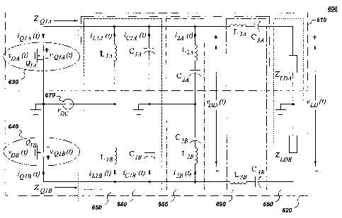
Referring to FIG. 6, a push-pull version of the class EF2 inverter is
depicted. The
circuit 600 consists of two single-ended class EF2 inverters 610, 620 (such as
shown
in FIG. 1) denoted by using subscripts A and B for each of the two converters,
with a
common ground reference and with the drive signals VDA and VDB operating 180
out
of phase. For the purpose of illustration, assume that the component values
remain the
same in each converter, e.g. C1 = CIA = CIB, C2 = C2A = C2B, etc. The output
voltage
VLD = 2VLD,SE and the output power is also doubled over that of the single-
ended case.
The impedance ZQI,, seen by each transistor, where x can be either A or B, is
the same
CA 02712879 2010-08-12
236153-1
as ZQ1 seen in the single-ended case, thus the waveforms for converter A and B
will be
the same.
Referring again to FIG. 6, each inverter section 610, 620 has a switching
section 630,
640 that in this example are transistors QIA, Q1B. There is a resonant network
section
650 including L1, C1, L2, C2, L3, C3 for each inverter section 610, 620
coupled to a
voltage source 670 and to the load 660. In more particular detail, the
resonator
network 650 in this example includes a first harmonic resonator section 680, a
second
harmonic resonator section 685 and a third harmonic resonator section 690.
Under normal operation, the converter 600 operates in periodic steady-state,
with the
fundamental period corresponding to the switching frequency Fs. Under this
condition, all waveforms are decomposed into integer multiples of Fs. For
illustrative
purposes, it is sufficient to consider the non-negative integers for the
harmonics,
which are denote by n E [0, oo). Furthermore, it is useful to separate the
frequency
components Fn into the even components Fe and odd components Fo.
Under this condition, one of the properties of the push-pull operation is that
even
frequency components Fe, including the DC component Fo, appear as common-mode
signals, whereas odd frequency components FO, including the fundamental F1 =
Fs,
appear as differential signals. Because the circuit is an inverter, only the
AC
component of the load is of interest.
Referring to the circuit 700 in FIG. 7, since the DC load component is common
mode
and thus flows in the ground, the ground separating the two loads ZLDA and
ZLDB can
be disconnected, thereby combining the loads ZLDA and ZLDB into a single load
710
that is ZLD = ZLDA + ZLDB = 2ZLD,SE. Note that in theory, this would affect
the switch
impedances ZQ1A and
ZQ1B at even frequency components and potentially affect the
operation. In practice however, the resonant networks formed by the
combinations of
L3A and C3A, and L3B and C3B, attenuate the second and higher harmonics of Fs
and
thus combining the load resistor into a single resistor as described has
minimal effect.
For the class EF2 circuit, any effect at the second harmonic is further
reduced by the
second harmonic shorts formed by L2, - C2,,.
11
CA 02712879 2010-08-12
236153-1
FIG. 8 shows the circuit 800 with dc feed inductors L1A and L1B from the first
resonator network combined to form a single center-tapped inductor 810. LIA
and LIB
denote substantially identical coupled windings with a coupling coefficient k1
between
0 and 1. Given that 0< k1 <1, even frequency components see a contribution
from the
leakage inductance between windings Lie = Llk, and odd frequency components
see the
sum of the leakage inductance and the mutual inductance Lio = Lik + LM. In the
ideal
case, k1= 1 and the windings are perfectly coupled (Lie = Lik = 0 and L10 =
LM). Then
the even harmonic components see a low impedance to ground, and the operation
becomes identical to class DE operation. While this is desirable, achieving
such good
coupling becomes impractical as the frequency increases. In this case, L10 is
designed
to present the necessary impedance to the odd frequency components for proper
operation, and the even frequency components, especially the second, can be
controlled by other components, as will be appreciated by the description
herein.
One of the advantage of coupling LIA and L1B is that if the windings are on a
common
magnetic core, the even frequency components of flux cancel in the core. This
reduces
core losses due to AC components, and because the DC flux component becomes
effectively zero, the AC flux swing in the core may be much larger, thereby
allowing a
smaller core and thus a smaller inductor.
Another advantage of coupling L1A and L1B as described herein is that since
the
winding are coupled, the odd-mode inductance is a superlinear function of the
number
of winding turns, approaching a function proportional to the turns squared as
k1
approaches unity. Since the odd-mode inductance required is twice that of the
single-
ended case, less than twice the turns are needed on the common core. This
reduces
both size and losses in the coupled inductors compared to two uncoupled
inductors.
FIG. 9 shows one embodiment of the present system with circuit 900. For
illustrative
purposes, each transistor has its own impedance that is developed by the
circuit. By
the modifications detailed herein, there are no longer two completely separate
inverter
circuits, and by employing the second harmonic trap it effectively shorts out
the
second harmonic. It is noted that the impedance seen at the terminal of each
transistor
is the same. The fundamental and odd harmonics are not affected by the
capacitance
12
CA 02712879 2010-08-12
236153-1
of the single C2 capacitor thereby providing a mechanism for tuning the
inverter
circuits.
Referring again to FIG. 9, in this embodiment C2A and C2B are combined into a
single
capacitor 910 for capacitance C2, by connecting L2A and L2B in series and
connecting
the center point between them to a capacitance C2 to ground. In the case where
L2A
and L2B are uncoupled, even frequency components will see an equivalent series
resonant network to ground consisting of C2 in series with an inductance Lee
L2/2,
where L2 = L2A = L2B. Odd frequency components will see an equivalent network
consisting an inductance Leo, = L2A + L2B. Thus, it becomes possible to
independently
control the effect of the network on even and odd frequency components, while
reducing the number of total components.
In particular, the inductors L2A and L2B are chosen to produce the desired
effect for the
odd frequency components, i.e. the fundamental Fs and the third harmonic 317s,
without needing to consider the behavior at the second harmonic 2Fs. Once the
inductor value is selected, capacitor C2 can be adjusted to provide the
desired low
impedance at the second harmonic 2Fs, without affecting the transistor
impedance at
the odd frequency components. Furthermore, because Class EF2 operation
requires a
low impedance at 2Fs, which is produced by the network of L2A, L2B, and C2.
This low
impedance will be negligibly affected by the impedance contribution of the
balance of
the components thus they can be adjusted without affecting substantially the
impedance at the second harmonic.
Although not shown explicitly in FIG. 9, L2A and L2B may be coupled similarly
to L1A
and L1B as described herein. By such coupling, it is possible to increase the
odd-mode
inductance and reduce the even-mode inductance. Increasing the odd-mode
inductance
reduces odd-mode currents in the second harmonic shorting network, reducing
losses
due to these currents. Reducing the even-mode inductance allows the use of a
larger
value of C2 to achieve the second harmonic short, which in turn reduces
voltage stress
on C2. The description regarding independent tuning of odd and even harmonics
apply
in this case.
13
CA 02712879 2010-08-12
236153-1
FIG. 10 shows another embodiment of the push-pull configuration 1000 that also
allows the roles of C2 and L2 to be reversed, and shows that the second
harmonic
resonator inductors L2A and L2B are combined into a single inductor 1010 for
inductance L2, by connecting C2A and C2B in series and connecting the center
point
between them to inductance L2 to ground. Even frequency components will see an
equivalent series resonant network to ground consisting of L2 in series with a
capacitance C2e = 2C2, where C2 = C2A = C2B. Odd frequency components will see
an
equivalent network consisting a capacitance C2o = C2/2. Thus, this provides
for
independently controlling the effect of the network on even and odd frequency
components while reducing the number of total components. This advantageously
allows another degree of design freedom.
Referring to FIG. 11, while inverters are detailed herein, substituting the
load ZLD with
a rectifier 1110 converts the AC output to DC, which in turn powers a load
RLD,
wherein a dc-dc converter is designed. As with the inverter, the single-ended
rectifier
1110 may be implemented as a push-pull version.
Referring to FIG. 12, the inductors L4A and L4B of the dc-dc converter of FIG.
11 are
implemented with coupled inductors 1210, with the same benefits as described
for L1A
and LIB on the inverter. This rectifier is a resonant push-pull rectifier.
The independent resonant harmonic adjusting network provided by the system
detailed herein has many applications. For example, the circuit and technique
can be
implemented in RF power amplifiers for the healthcare industry. Another
application
is for communications transmissions, such as an FM transmitter, wherein the
improved efficiency provides cost savings in operations. A further application
involves medical applications and operation with a switching frequency up to
300MHz.
In dc-dc power conversion applications, such as push-pull topologies, the
advantages
include increasing the switching frequency while minimizing the detriments of
the
prior attempts. Other features include combining parallel coupled capacitors
and
splitting inductors, thereby reducing the component count. Another aspect
includes
lowering the number of windings due to the lower inductance requirements
thereby
14
CA 02712879 2010-08-12
236153-1
using less precious metals, such as copper. In addition, since there are less
windings,
the leakage inductance is lower and can be integrated as part of the network.
Some of the advantages of the present system include the manufacturability of
power
processors that are much smaller, such as 2 - 10 times smaller due to the
innovative
structure. One feature that distinguishes the design of the present system is
the ability
to cancel dc current in the inductors of the resonant networks. Another
feature
includes the ability to independently control impedances seen by the
transistors for
even and odd harmonics. Another distinction includes an increase of the input
and
output ripple frequency, such as doubling the input and output ripple
frequency,
thereby reducing filtering requirements.
The foregoing description of the embodiments of the invention has been
presented for
the purposes of illustration and description. It is not intended to be
exhaustive or to
limit the invention to the precise form disclosed. Many modifications and
variations
are possible in light of this disclosure. It is intended that the scope of the
invention be
limited not by this detailed description, but rather by the claims appended
hereto.