Note: Descriptions are shown in the official language in which they were submitted.
CA 02712893 2015-10-23
= = =
SYSTEM AND METHOD FOR COMMUNICATING WITH AN IMPLANT
BACKGROUND OF THE INVENTION
FIELD OF THE INVENTION
[0002] The present invention relates generally to orthopaedic implants
and more
particularly to orthopaedic implants that incorporate a portion of a radio
telemetry system.
RELATED ART
[0003] Trauma products, such as intramedulltuy (IM) nails, pins, rods,
screws, plates
and staples, have been used for many years in the field of orthopaedics for
the repair of broken
bones. These devices function well in most instances, and fracture healing
occurs more
predictably than if no implant is used. In some instances, however, improper
installation,
implant failure, infection or other conditions, such as patient non-compliance
with prescribed
post-operative treatment, may contribute to compromised healing of the
fracture, as well as
increased risk to the health of the patient.
[0004] Health care professionals currently use non-invasive methods,
such as x-rays,
to examine fracture healing progress and assess condition of implanted
devices. However, x-
rays may be inadequate for accurate diagnoses. They are costly, and repeated x-
rays may be
detrimental to the patient's and health care workers' health. In some cases,
non-unions of
fractures may go clinically undetected until implant failure. Moreover, x-rays
may not be used
to adequately diagnose soft tissue conditions or stress on the implant. In
some instances,
invasive procedures are required to diagnose implant failure early enough that
appropriate
remedial measures may be implemented.
1
CA 02712893 2010-07-21
WO 2009/097485
PCT/US2009/032540
[0005]
The trauma fixation implants currently available on the market are passive
devices because their primary function is to support the patient's weight with
an appropriate
amount of stability whilst the surrounding fractured bone heals. Current
methods of assessing
the healing process, for example using radiography or patient testimonial do
not provide
physicians with sufficient information to adequately assess the progress of
healing,
particularly in the early stages of healing. X-ray images only show callus
geometry and cannot
access the mechanical properties of the consolidating bone. Therefore, it is
impossible to
quantify the load sharing between implant and bone during fracture healing
from standard
radiographs, CT, or MRI scans. Unfortunately, there is no in vivo data
available quantifying
the skeletal loads encountered during fracture healing as well as during
different patient and
physiotherapy activities. The clinician could use this information to counsel
the patient on life-
style changes or to prescribe therapeutic treatments if available. Continuous
and accurate
information from the implant during rehabilitation would help to optimize
postoperative
protocols for proper fracture healing and implant protection and add
significant value in
trauma therapy. Furthermore, improvements in security, geometry, and speed of
fracture
healing will lead to significant economic and social benefits. Therefore, an
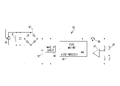
opportunity exists
to augment the primary function of trauma implants to enhance the information
available to
clinicians.
[0006]
Patient wellness before and after an intervention is paramount. Knowledge of
the patient's condition can help the caregiver decide what form of treatment
may be necessary
given that the patient and caregiver are able to interact in an immediate
fashion when
necessary. Many times the caregiver does not know the status of a would-be or
existing patient
and, therefore, may only be able to provide information or incite after it was
necessary. If
given information earlier, the caregiver can act earlier. Further, the earlier
information
potentially allows a device to autonomously resolve issues or remotely perform
the treatment
based on a series of inputs.
2
CA 02712893 2010-07-21
WO 2009/097485
PCT/US2009/032540
[0007] Surgeons have historically found it difficult to assess the
patient's bone healing
status during follow up clinic visits. It would be beneficial if there was a
device that allowed
the health care provider and patient to monitor the healing cascade. Moreover,
it would be
beneficial if such a device could assist in developing custom care therapies
and/or
rehabilitation.
[0008]
Wireless technology in devices such as pagers and hand-held instruments has
long been exploited by the healthcare sector. However, skepticism of the risks
associated
with wireless power and communication systems has prevented widespread
adoption,
particularly in orthopaedic applications. Now, significant advances in
microelectronics and
performance have eroded many of these perceived risks to the point that
wireless technology
is a proven contender for high integrity medical systems. Today's medical
devices face an
increasingly demanding and competitive market. As performance targets within
the sector
continue to rise, new ways of increasing efficiency, productivity and
usability are sought.
Wireless technology allows for two-way communication or telemetry between
implantable
electronic devices and an external reader device and provides tangible and
recognized
benefits for medical products and is a key technology that few manufacturers
are ignoring.
[0009]
Currently, Radio Frequency (RF) telemetry and inductive coupling systems
are the most commonly used methods for transmitting power and electronic data
between the
implant and the companion reader. Implantable telemetric medical devices
typically utilize
radio-frequency energy to enable two way communications between the implant
and an
external reader system. Although data transmission ranges in excess of 30m
have been
observed previously, energy coupling ranges are typically reduced to a couple
of inches using
wireless magnetic induction making these implants unsuitable for commercial
application.
Power coupling issues can be minimized using a self-contained lithium battery,
which are
typically used in active implantable devices such as pacemakers, insulin
pumps,
neurostimulators and cochlea implants. However, a re-implantation procedure
must be
3
CA 02712893 2010-07-21
WO 2009/097485
PCT/US2009/032540
performed when the battery is exhausted, and a patient obviously would prefer
not to undergo
such a procedure if possible.
[0010] Some telemetric systems include electronics and/or an antenna.
In general,
these items must be hermetically sealed to a high standard because many
electronic
components contain toxic compounds, some electronic components need to be
protected from
moisture, and ferrite components, such as the antenna, may be corroded by
bodily fluids,
potentially leading to local toxicity issues. Many polymers are sufficiently
biocompatible for
long-term implantation but are not sufficiently impermeable and cannot be used
as
encapsulants or sealing agents. In general, metals, glasses, and some ceramics
are
impermeable over long timescales and may be better suited for use in
encapsulating implant
components in some instances.
[0011] Additionally, surgeons have found it difficult to manage
patient information. It
would be beneficial if there was available a storage device that stored
patient information,
such as entire medical history files, fracture specifics, surgery performed, X-
ray images,
implant information, including manufacturer, size, material, etc. Further, it
would be beneficial
if such storage device could store comments/notes from a health care provider
regarding
patient check-ups and treatments given.
SUMMARY OF THE INVENTION
[0012] According to some aspects of the present invention there may be
provided a
system for communicating patient information. The system may include a medical
implant, the
medical implant has a first cavity and a second cavity, the first and second
cavity connected by
one or more apertures, the first cavity is adapted to receive on-board
electronics, the on-board
electronics comprising at least one sensor, a microprocessor, and a data
transmitter, and the
second cavity is adapted to receive an implant antenna; a signal generator
adapted to generate a
first signal; an amplifier electrically connected to the signal generator; at
least one coil electrically
connected to the amplifier; a receiver adapted to receive a data packet having
data from the
4
CA 02712893 2010-07-21
WO 2009/097485
PCT/US2009/032540
implant antenna; and a processor connected to the receiver; wherein the signal
generator
generates the first signal, the amplifier amplifies the first signal, the at
least one coil transmits the
amplified signal, the implant antenna receives the first signal and transmits
a data packet
containing data, the receiver receives the data packet, and the processor
either processes the data
or sends the data to a data storage device.
[0013] According to some embodiments, the processor is selected from
the group
consisting of a desktop computer, a laptop computer, a personal data
assistant, a mobile handheld
device, and a dedicated device.
[0014] According to some embodiments, the receiver may be an antenna
with an adapter
for connection to the processor.
[0015] According to some embodiments, the on-board electronics may
include a plurality
of sensor assemblies and a multiplexer.
[0016] According to some embodiments, the at least one coil may be a
transmission coil.
[0017] According to some embodiments, there are two coils, and the
coils are housed
within a paddle.
[0018] According to some embodiments, the system further includes a
control unit, and
wherein the signal generator and the amplifier are housed within the control
unit.
[0019] According to some embodiments, the system further includes one
or more
components selected from the group consisting of a feedback indicator, a load
scale, a portable
storage device, a second processor.
[0020] According to some embodiments, the first signal has a frequency
of about 125
kHz.
[0021] According to some embodiments, the first cavity and the second
cavity are
orthogonal to one another.
[0022] According to some embodiments, the first cavity and the second
cavity are
diametrically opposed.
5
CA 02712893 2010-07-21
WO 2009/097485
PCT/US2009/032540
[0023] According to some embodiments, at least one of the first cavity
and the second
cavity further includes a cover.
[0024] According to some embodiments, the on-board electronics
comprise an LC
circuit, a bridge rectifier, a storage capacitor, a wake up circuit, a
microprocessor, an enable
measurement switch, an amplifier, a Wheatstone bridge assembly, and a
modulation switch.
[0025] According to some embodiments, the microprocessor may include
an analog to
digital converter.
[0026] According to some embodiments, the modulation switch may
modulate a load
signal. According to some embodiments, the load signal may be modulated at a
frequency
between 5 kHz and 6 kHz.
[0027] The invention includes a system having a telemetric implant.
The telemetric
implant is capable of receiving power wirelessly from an external reader at a
distance using
sophisticated digital electronics, on board software, and radio frequency
signal filtering. The
implant may be equipped with at least one sensor, interface circuitry, micro-
controller,
wakeup circuit, high powered transistors, printed circuit board, data
transmitter and power
receive coil with software algorithm, all of which may be embedded in machined
cavities
located on the implant. The telemetry system may use a coiled ferrite antenna
housed and
protected inside the metallic body of the implant using a metal encapsulation
technique
suitable for long term implantation. The use of digital electronics and a high
permeable
material located inside a metallic cavity compensates for the effect of
severely shielding a
power coil from the externally applied magnetic power field. The digital
electronics enables
multiplexing to read multiple sensors. The electronics module does not require
the reader to
be positioned within a pre-defined "sweet spot" over the implant in order to
achieve a stable
reading relating to sensed data minimizing the potential to collect erroneous
measurements.
[0028] Further areas of applicability of the invention will become apparent
from the
detailed description provided hereinafter. It should be understood that the
detailed
6
CA 02712893 2010-07-21
WO 2009/097485
PCT/US2009/032540
description and specific examples, while indicating the particular embodiment
of the
invention, are intended for purposes of illustration only and are not intended
to limit the
scope of the invention.
BRIEF DESCRIPTION OF THE DRAWINGS
[0029] The accompanying drawings, which are incorporated in and form a part
of the
specification, illustrate the embodiments of the present invention and
together with the
written description serve to explain the principles, characteristics, and
features of the
invention. In the drawings:
[0030] FIG. 1 illustrates a first system for communicating with an
implant;
[0031] FIG. 2 illustrates a block diagram for power harvesting;
[0032] FIG. 3 illustrates a block diagram for signal transmission;
[0033] FIG. 4 illustrates an exemplary data packet structure;
[0034] FIG. 5 illustrates an exemplary receiver circuit board;
[0035] FIG. 6 illustrates a flowchart showing the reader steps;
[0036] FIG. 7 illustrates an exemplary electrical diagram of the implant
electronics;
[0037] FIG. 8 illustrates a flowchart showing the steps of sensor
measurement;
[0038] FIG 9 illustrates a first embodiment of on-board implant
electronics;
[0039] FIG. 10 illustrates a second embodiment of on-board implant
electronics;
[0040] FIGS. 11-14 illustrate one particular embodiment of the
orthopaedic implant;
[0041] FIG. 15 illustrates a first cavity and a second cavity;
[0042] FIGS. 16-23 illustrate assembly of the orthopaedic implant
shown in FIGS.
11-14;
[0043] FIG. 24 illustrates a second system for communicating with an
implant;
[0044] FIG. 25 illustrates a coil;
[0045] FIG. 26 illustrates a third system for communicating with an
implant;
[0046] FIG. 27illustrates a paddle;
7
CA 02712893 2010-07-21
WO 2009/097485
PCT/US2009/032540
[0047] FIG. 28 illustrates a wiring diagram of the paddle and the
receiver;
[0048] FIG. 29 illustrates a fourth system for communicating with an
implant;
[0049] FIG. 30 is a graph illustrating the received signal of the
fourth system;
[0050] FIG. 31 illustrates a data storage system; and
[0051] FIG. 32 illustrates a health care facility with one or more kiosks.
DETAILED DESCRIPTION OF THE EMBODIMENTS
[0052] The following description of the depicted embodiment(s) is
merely exemplary
in nature and is in no way intended to limit the invention, its application,
or uses.
[0053] A "smart implant" is an implant that is able to sense its
environment, apply
intelligence to determine whether action is required, and possibly act on the
sensed
information to change something in a controlled, beneficial manner. This would
ideally occur
in a closed feedback loop reducing the chance of coming to an erroneous
conclusion when
evaluating the sensed data. One attractive application of smart implant
technology is to
measure loads on an orthopaedic implant. For example, an intramedullary nail
subjected to six
spacial degrees of freedom, comprised of 3 forces (Axial Force, Fz, Shear
Force Fx & Fy) and
3 moments (Mx-bending, My-bending and Mz-torsional) may be measured indirectly
by
measuring sensor output of a series of strain gauges mounted to the
orthopaedic implant using
the matrix method.
[0054] FIG. 1 illustrates a system 10 for communicating with an
implant in a first
embodiment. The system 10 includes an orthopaedic implant 12, a coil 14, a
signal generator
15, an amplifier 16, a data packet 18, a processor 20, and a receiver 22. In
the depicted
embodiment, the orthopaedic implant is an intramedullary nail but other types
of orthopaedic
implants may equally be used. As examples, the orthopaedic implant may be an
intramedullary nail, a bone plate, a hip prosthetic, or a knee prosthetic.
Further, the processor
20 is depicted as a desktop computer in FIG. 1 but other types of computing
devices may
equally be used. As examples, the processor 20 may be a desktop computer, a
laptop
8
CA 02712893 2010-07-21
WO 2009/097485
PCT/US2009/032540
computer, a personal data assistant (PDA), mobile handheld device, or a
dedicated device. In
some embodiments, the processor 20 and the receiver 22 form a single
component. In the
depicted embodiment, however, the receiver 22 is electrically connected to the
processor 20
but is a separate component. As examples, the receiver 22 may be an antenna
with an adapter
to connect to a computer port or a wireless interface controller (also known
as a wireless
card) for connection to the processor 20, such as through the use of a PCI
bus, mini PCI, PCI
Express Mini Card, USB port, or PC Card. As is explained in greater detail
below, the signal
generator 15 generates a signal, the amplifier 16 amplifies the signal, the
coil 14 transmits the
amplified signal, the orthopaedic implant 12 receives the signal and transmits
a data packet
18 containing data, the receiver 22 receives the data packet, and the
processor 20 may either
process the data or send the data to a storage device (not shown).
[0055] The
orthopaedic implant 12 may incorporate one or more power management
strategies. Power management strategies may include implanted power sources or
inductive
power sources. Implanted power sources may be something simple, such as a
battery, or
something more complex, such as energy scavenging devices. Energy scavenging
devices
may include motion powered piezoelectric or electromagnetic generators and
associated
charge storage devices. Inductive power sources include inductive coupling
systems and
Radio Frequency (RF) electromagnetic fields. The orthopaedic implant 12 may
incorporate a
storage device (not shown). The storage device may be charged by an
inductive/RF coupling
or by an internal energy scavenging device. Preferably, the storage device has
sufficient
capacity to store enough energy at least to perform a single shot measurement
and to
subsequently process and communicate the result.
[0056] In
some embodiments, the orthopaedic implant 12 may be inductively
powered. FIG. 2 illustrates an exemplary block diagram for harvesting power
from the
amplified signal. The assembled components, which may form a portion of
printed circuit
board or a separate assembly, generally is referred to as a power harvester
30. The power
9
CA 02712893 2010-07-21
WO 2009/097485
PCT/US2009/032540
harvester 30 includes an antenna 32, a rectifier 34, and a storage device 36.
In the depicted
embodiment, the storage device 36 is a capacitor but other devices may be
used.
[0057] In
some embodiments, the orthopaedic implant 12 may include an onboard
microchip that converts signals from analog to digital and sends the digital
signal via a radio
wave. FIG. 3 illustrates an exemplary block diagram of a microchip 40 for
signal conversion
and signal transmission. The microchip 40 also may be termed a
microcontroller. The
microchip 40 includes a converter 42, a processor 44, a transmitter 46, and an
antenna 48.
The converter 42 converts analog signals to digital signals. The processor 44
is electrically
connected to the converter 42. In some embodiments, the processor 44 is also
connected to an
input/output port 41. The transmitter 46 is electrically connected to the
processor 44 and to
the antenna 48. In some embodiments, the transmitter 46 is replaced by a
transceiver that is
capable of transmitting and receiving signals. In the depicted embodiment, the
transmitter 46
transmits in the ultra-high frequency (UHF) range but those of ordinary skill
in the art would
understand that other ranges may equally be used. Further, while in FIG. 3 the
transmitter 46
is depicted as a radio chip, other methods and devices for sending a radio
wave may be used.
[0058] The
transmitter 44 transmits data in the form of a packet. At a minimum, the
packet includes control information and the actual data. FIG. 4 illustrates an
exemplary
digital data packet structure 18. The data packet structure 18 includes a pre-
amble 52, a sync
flag 54, an implant identifier 56, data 58, and error checking data 59. The
pre-amble 52
initializes the receiver, and the sync flag 54 detects the incoming packet.
The telemetry data
58 may be any physical measurement, such as implant forces, implant micro-
motion, implant
position, alkalinity, temperature, pressure, etc. The error checking data 59
is used to verify
the accuracy of the data packet. For example, the error checking data 59 may
contain a value
to calculate a checksum or cyclic redundancy check. If the data is corrupted,
it may be
discarded or repaired. In some embodiments, the data packet 18 also may
include a length
field that provides data as to the length of the packet. For example, if the
implant has multiple
CA 02712893 2010-07-21
WO 2009/097485
PCT/US2009/032540
sensors, then length field may indicate a larger data packet than if the
implant has only a
single sensor. In some embodiments, the data packet structure may include
fields for
encryption.
[0059]
FIG. 5 illustrates an example of the receiver 22. In the depicted embodiment,
the receiver 22 is a USB wireless adapter capable of receiving radio waves
adapted for
connection to the processor 20. For example, the USB wireless adapter may be a
development board having a microcontroller with on-board flash memory and USB
interface
support to provide a flexible platform for software development, such as the
AT9OUSB1286
development board available from ATMEL Corporation, 2325 Orchard Parkway, San
Jose,
California 95131. The receiver 22 may include software such that it is
recognized by the
processor 20 as a USB mass storage device. The receiver 22 may be used to
develop
"Software Defined Radio" (SDR) demodulation. An SDR system is a radio
communication
system that can potentially tune to any frequency band and receive any
modulation across a
large frequency spectrum through the use of as little hardware as possible and
processing the
signals through software.
[0060]
FIG. 6 illustrates an exemplary flowchart depicting the steps that may be
taken
by the receiver 22 upon receipt of the data packet structure 18 and
initialization by the pre-
amble field 52. In step 150, the receiver 22 recognizes the sync field 52. In
optional step 152,
the receiver 22 may read the length field. In step 154, the receiver 22
decodes the
identification field 56. Step 154 may involve reference to a look-up table to
match the
identification field to a stored set of data. For example, the receiver may
match the
identification field with an entry in a database which contains information on
the implant
and/or the patient. Optional step 156 is decision whether or not the
identification field is
recognized. If the identification field is not recognized, the data packet may
be rejected.
Otherwise, the receiver proceeds to step 158. In step 158, the data 58 is
read. In step 160, the
error checking data 59 is calculated. In step 162, there is a decision as
whether the data is
11
CA 02712893 2010-07-21
WO 2009/097485
PCT/US2009/032540
error free. If the data packet contains an error, then the packet is rejected.
Otherwise, the data
is output to the processor 20, either through wire or wirelessly. As examples,
the data may be
output through a serial port or universal serial bus.
[0061] In
some embodiments, the orthopaedic implant 12 includes on-board
electronics for power harvesting, sensing data, processing of the sensed data,
and data
transmission. FIG. 7 illustrates an exemplary wiring diagram of a circuit 60.
The circuit 60
includes an LC circuit 61, a bridge rectifier 62, a storage capacitor 63, a
wake up circuit 64, a
microprocessor 65, an enable measurement switch 66, an amplifier 67, a sensor
and wheat
stone bridge assembly 68, and a modulation switch 69. In the depicted
embodiment, the
wake up circuit 64 compares working voltage to stored voltage to see if the
stored voltage
reaches a certain threshold. As an example, the microprocessor 65 has a clock
speed of 128
khz.
[0062] The
LC circuit 61 receives a carrier signal from the antenna 14 to inductively
power the on-board electronics. As an example, the carrier signal may have a
frequency of
about 125 kHz. The use of inductive power eliminates the requirement for a
battery in the
telemetric implant 12. In the depicted embodiment, the storage capacitor 63, a
battery (not
shown) or other energy storage device may be used to power the on-board
electronics when
not inductively powered. In other embodiments, the on-board electronics
operate only when
powered inductively from the antenna 14. The circuit 60 does not transmit raw
data to the
receiver 22 but instead modulates a load signal. This technique uses less
power than raw
transmission. The signal can be modulated using software embedded in the
microprocessor
65. The load signal is related to the amount of resistance measured by the
sensor assembly
68. In the depicted embodiment, the load signal is modulated at a frequency
between 5 kHz
and 6 kHz but those skilled in the art would understand that other frequency
bands may be
used. The change in load on the telemetric implant 12 is transmitted by the LC
circuit 61 and
received by the receiver 22.
12
CA 02712893 2010-07-21
WO 2009/097485
PCT/US2009/032540
[0063]
FIG. 8 is a flowchart that illustrates the steps taken within the circuit 60
for
sensor measurement. In step 170, there is provided a wake-up interrupt by the
wake up circuit
64. The wake up circuit 64 engages the enable measurement switch 66 in step
172 when the
stored voltage reaches a certain threshold. This enables the sensor assembly
68 and powers
the amplifier 67. The microprocessor 65 takes readings in step 174. The
microprocessor 65
includes an analog-to-digital converter that converts the analog signal from
the sensor
assembly to a digital signal. In step 176, the microprocessor 65 forms a data
packet, and
generates an error checking data in step 178. In step 180, the microprocessor
65 outputs the
data packet. In some embodiments, this may be accomplished by transmitting the
data via a
radio chip. In the embodiment depicted in FIG. 7, the microprocessor 65
selectively opens
and closes the modulation switch 69 to send out the data via the LC circuit
61. In step 182,
there is a decision whether there is sufficient power to resend the data
packet. If so, the
process loops back to step 180 to resend the data packet until all of the
energy stored in the
storage device 63 has been used. When there is no longer sufficient power to
resend the data
packet, the process stops in step 184. In the depicted embodiment, the wake up
circuit 64
turns on above 3 volts and shuts down below 2 volts.
[0064]
FIG. 9 schematically illustrates a first embodiment of on-board implant
electronics 70. In FIG. 9, some components, such as a power supply, have been
removed for
clarity. The on-board implant electronics 70 includes a sensor and wheatstone
bridge
assembly 72, an amplifier 74, a microprocessor 76, and a transmitter 78. In
the depicted
embodiment, the sensor assembly 72 includes a foil gauge connected to a
wheatstone bridge.
Alternatively, the sensor may be a semiconductor or thin film strain gauge.
The sensor
assembly 72 may include any number of types of sensors including, but not
limited to, a foil
strain gauge, a semi-conductor strain gauge, a vibrating beam sensor, a force
sensor, a
piezoelectric element, a fibre Bragg grating, a gyrocompass, or a giant
magneto-impedance
(GMI) sensor. Further, the sensor may indicate any kind of condition
including, but not
13
CA 02712893 2010-07-21
WO 2009/097485
PCT/US2009/032540
limited to, strain, pH, temperature, pressure, displacement, flow,
acceleration, direction,
acoustic emissions, voltage, electrical impedance, pulse, biomarker
indications, such as a
specific protein indications, chemical presence, such as by an oxygen
detector, by an oxygen
potential detector, or by a carbon dioxide detector, a metabolic activity, or
biologic
indications to indicate the presence of white blood cells, red blood cell,
platelets, growth
factors, or collagens. Finally, the sensor may be an image capturing device.
The
microprocessor 76 includes an analog-to-digital converter that converts the
analog signal
from the sensor assembly to a digital signal. When the sensor assembly 72 is
powered, the
sensor assembly 72 sends a signal to the amplifier 74, which amplifies the
signal. The
amplified signal is sent to the microprocessor 76, which converts the signal
from analog to
digital. The microprocessor forms a data packet from the digital signal and
transmits the data
packet via the transmitter 78.
[0065]
FIG. 10 schematically illustrates a second embodiment of on-board implant
electronics 80. In FIG. 10, some components, such as a power supply, have been
removed for
clarity. The on-board implant electronics 80 includes a plurality of sensor
and wheatstone
bridge assemblies 82, a multiplexer 83, an amplifier 84, a microprocessor 86,
and a
transmitter 88. In its simplest form, the multiplexer 83 is an addressable
switch. The
multiplexer 83 is linked to the microprocessor and selects the sensor from
which to receive
data. In the depicted embodiment, the sensor assembly 82 includes a foil gauge
connected to
a wheatstone bridge. Alternatively, the sensor may be a semiconductor strain
gauge. The
microprocessor 86 includes an analog-to-digital converter that converts the
analog signal
from the sensor assembly to a digital signal. When the sensor assemblies 82
are powered,
each sensor assembly 82 sends a signal to the multiplexer 83. The multiplexer
83 sends the
multiplexed signal to the amplifier 84, which amplifies the signal. The
amplified signal is
sent to the microprocessor 86, which converts the signal from analog to
digital. The
microprocessor forms a data packet from the digital signal and transmits the
data packet via
14
CA 02712893 2010-07-21
WO 2009/097485
PCT/US2009/032540
the transmitter 88. While only two sensor assemblies are shown in FIG. 10,
those having
ordinary skill in the art would understand that the implant 12 may have more
than two sensor
assemblies and may be limited only by the size and shape of the implant.
Further, the
configuration of the sensors also may be tailored to meet the requirements of
the patient's
fracture.
[0066]
FIGS. 11-14 illustrate one particular embodiment of the orthopaedic implant
12. In the depicted embodiment, the orthopaedic implant 12 is an
intramedullary nail but
other implant types may be used. The orthopaedic implant 12 may include one or
more
cavities to receive on-board electronics. Alternatively, the cavities may be
termed "pockets."
In the embodiment depicted in FIG. 11, the orthopaedic implant 12 includes a
first cavity 90
and a second cavity 92. While in the depicted embodiment the first cavity 90
is generally
orthogonal to the second cavity 92, those having ordinary skill in the art
would understand
that other arrangements are possible. For example, the first cavity 90 may be
diametrically
opposed to the second cavity 92. The first cavity 90 is adapted to receive on-
board electronics
100, and the second cavity 92 is adapted to receive an antenna 110. Of course,
these
component locations may be reversed. Further, both components may be located
within a
single cavity in some embodiments. In some embodiments, the cavity may be
tapered to
match the overall shape of the implant. The use of multiple cavities allows
for different
methods of encapsulation for each cavity. Different methods of encapsulation
may be
required depending upon the materials used.
[0067]
FIG. 12 illustrates an exemplary embodiment of the on-board electronics 100.
The orthopaedic implant 12 may include one or more covers corresponding to the
one or
more cavities. In the embodiment depicted in FIGS. 13 and 14, there is
provided a first cover
120 corresponding to the first cavity 90 and a second cover 122 corresponding
to the second
cavity 92. The one or more cavities may include a steeped recess to receive
the cover. The
cover is made from a biocompatible material. As examples, the cover may be
made from
CA 02712893 2010-07-21
WO 2009/097485
PCT/US2009/032540
titanium, stainless steel, shape memory alloy, or ceramic. Ceramics may
include alumina,
zirconia, boron nitride, or machinable aluminium nitride. In the embodiment
depicted in
FIGS. 13 and 14, the covers 120, 122 have a thickness in the range from about
43 microns to
about 0.5 millimeters but of course other dimensions may be used. In some
embodiments, a
metal cover may affect the performance of the antenna, and therefore the
electronics cavity
may have a metal cover while the antenna has a ceramic cover. In some
embodiments, the
cover may include a ceramic central portion vapor deposited on a flange frame
made of
metal, such as titanium. In other embodiments, the cover may include a central
foil portion
and a metal flange frame to reduce the risk of signal loss.
[0068] Consideration
may be given to the location and size of the one or more
cavities. The cavities should be conveniently placed but not significantly
affect the structural
integrity of the orthopaedic implant 12. Finite element analysis may be of use
in judging
appropriate cavity location and dimensions. Factors which may be considered
include: (1)
geometry of the implant; (2) symmetry of the implant (e.g., left and right
implants); (3)
whether the cavity provides a convenient location for data transmission and/or
reception; (4)
whether a sensor will be located in the same cavity as the embedded antenna
coil; and (5)
location of the largest bending moment applied to the implant. These factors
are not all
inclusive, and other factors may be of significance. Similar factors may be
used to judge the
dimensions of the one or more cavities. In the embodiment depicted in FIG. 15,
the first
cavity 90 is about 20 millimeters in length, about 5 millimeters in width, and
about 3
millimeters in depth, and the second cavity 92 is about 30 millimeters in
length, about 5
millimeters in width, and about 3 millimeters in depth. Other dimensions,
however, may be
equally used.
[0069]
FIGS. 16-23 illustrate assembly of the orthopaedic implant 12 shown in FIGS.
11-14. As best seen in FIG. 16, one or more connection apertures 130 are
placed in the
implant 12 to connect the first cavity 90 to the second cavity 92. In some
embodiments, the
16
CA 02712893 2010-07-21
WO 2009/097485
PCT/US2009/032540
connection apertures 130 may be used to backfill the second cavity 92 with a
polymer
encapsulant (such as an epoxy or silicone elastomer) after attachment of the
cover.
Connectors 132 are placed in the holes 130 and may be affixed to the implant
12. For
example, the connectors may be gold-brazed or laser welded to the implant. The
implant 12
includes the biocompatible antenna 110. The antenna 110 includes a core 138
and wire 140
wrapped about the core. The core 138, which may be cylindrical or square-
shaped in cross-
section, includes a magnetically permeable material, such as ferrite. In FIG.
19, the core 138
is formed by a ferrite rod 134 placed within a borosilicate glass tube 136 but
other materials
or biocompatible coatings may be used. For example, the ferrite rod may be
coated with a
polyxylylene polymer, such as Parylene C. The glass tube 136 is sealed to
contain the ferrite
to make the core substantially biocompatible. For example, the glass tube may
be sealed
using an infrared laser. In some embodiments, the ferrite rod and/or the glass
tube may be
processed to include substantially planar portions for a better fit within the
cavity. The core
138 is wrapped with wire 140, such as copper wire or gold plated steel wire.
In the
embodiment depicted in FIG. 21, there is about 300 turns of wire wrapped about
the core
138. In an alternative embodiment, the wire 140 is wrapped about a ferrite rod
and sealed
within a glass tube while still allowing for external connection of the wire.
[0070] In
addition or in the alternative, the on-board electronics and/or the antenna
may be sealed by: (1) a compressed/deformed gold gasket to produce a hermetic
seal; (2)
electroplating over an epoxy capsule to produce a hermetic seal; (3) welding a
ceramic lid
with a metalized perimeter over the pick-up recess; or (4) coating the ferrite
using a vapor-
deposited material/ceramic.
[0071] As
best seen in FIG. 22, the on-board electronics 100 is placed in the first
cavity 90, and the antenna 110 is placed in the second cavity 92. In some
embodiments, a
sensor is placed under the on-board electronics 100. The on-board electronics
100 is
electrically connected to the antenna 110 via the connectors 132. The on-board
electronics
17
CA 02712893 2010-07-21
WO 2009/097485
PCT/US2009/032540
100 and/or the antenna 110 may be fixed in the cavities 90, 92 using a range
of high stiffness
adhesives or polymers including silicone elastomers, epoxy resins,
polyurethanes, polymethyl
methacrylate, ultra high density polyethylene terephthalate,
polyetheretherketone, UV curable
adhesives, and medical grade cyanoacrylates. As an example, EPO-TEK 301
available from
Epoxy Technology, 14 Fortune Drive, Billerica, Massachusetts 01821. These
types of
fixation methods do not adversely affect the performance of the electrical
components. In
some embodiments, the cavities may include under cuts or a dovetail groove to
hold the
adhesive or polymer in place. Thereafter, the covers 120, 122 are placed on
the implant 12
and welded in-place. For example, the covers may be laser welded to the
implant.
[0072] FIG. 24
illustrates a system 210 for communicating with an implant in a
second embodiment. The system 210 includes an orthopaedic implant 212, a coil
214, a
signal generator 215, an amplifier 216, a data packet 218, a processor 220,
and a receiver
222. In the depicted embodiment, the orthopaedic implant 212 is an
intramedullary nail but
other types of orthopaedic implants may equally be used. As examples, the
orthopaedic
implant 212 may be an intramedullary nail, a bone plate, a hip prosthetic, or
a knee
prosthetic. Further, the processor 220 may be a desktop computer, a laptop
computer, a
personal data assistant (PDA), mobile handheld device, or a dedicated device.
In some
embodiments, the processor 220 and the receiver 222 form a single component.
In the
depicted embodiment, however, the receiver 222 is electrically connected to
the processor
220 but is a separate component. The system 210 is similar to system 10 except
that instead
of the data packet being received by an antenna on the receiver 22, the data
packet is received
by the transmission coil 214 and sent by wire to the receiver 222.
Alternatively, the coil 214
may be wirelessly connected to the receiver 222. Further, the coil 214, the
amplifier 216,
and/or the signal generator 215 may form a single component.
[0073] FIG. 25
illustrates the coil 214. In FIG. 25, the coil 214 is formed by a plastic
spool wound with conductive wire. In the depicted embodiment, at least 60
turns of copper
18
CA 02712893 2010-07-21
WO 2009/097485
PCT/US2009/032540
wire having a diameter of about 0.4 mm is wound onto the plastic spool, and
the plastic spool
has an inner diameter of about 100 mm, an outer diameter of about 140 mm, and
a thickness
of about 8 mm thickness using a semi-automated coil winding machine. However,
these
dimensions are merely exemplary and those having ordinary skill in the art
would understand
that other dimensions might be used.
[0074]
FIG. 26 illustrates a system 310 for communicating with an implant in a third
embodiment. The system 310 includes an orthopaedic implant 312, a paddle 314,
a data
packet 318, a first processor 320, and a control unit 322. In the depicted
embodiment, the
orthopaedic implant 312 is an intramedullary nail but other types of
orthopaedic implants
may equally be used. As examples, the orthopaedic implant 312 may be an
intramedullary
nail, a bone plate, a hip prosthetic, or a knee prosthetic. Further, the first
processor 320 may
be a desktop computer, a laptop computer, a personal data assistant (PDA),
mobile handheld
device, or a dedicated device. In some embodiments, the first processor 320
and the control
unit 322 form a single component. In the depicted embodiment, however, the
control unit 322
is electrically connected to the processor 320 but is a separate component.
Optionally, the
system 310 also may include a feedback indicator 324, a load scale 326, a
portable storage
device 328, and/or a second processor 330. The load scale 326 provides a
reference for
comparison. For example, in the case of an intramedullary nail, the load scale
326 may be
used to compare the load applied to the patient's limb in comparison to the
load placed on the
intramedullary nail. As an example, the portable storage device 328 may be a
flash memory
device and may be integrated with a universal serial bus (USB) connector. The
portable
storage device 328 may be used to transfer data from the control unit 322 to a
processor or
from one processor to another. Moreover, the control unit 322 may be networked
or
incorporate a wireless personal network protocol.
[0075] The control
unit 322 transmits a signal, the orthopaedic implant 12 receives
the signal and transmits a data packet 318 containing data, the receiver 322
receives the data
19
CA 02712893 2010-07-21
WO 2009/097485
PCT/US2009/032540
packet, and the processor 320 may either process the data or send the data to
a storage device
(not shown). As an example, the transmitted signal may be in the range from
about 100 kHz
to about 135 kHz.
[0076] The
control unit 322 may transmit information by wire or wirelessly. The
control unit 322 may use available technologies, such as ZIGBEETm,
BLUETOOTHTm,
Matrix technology developed by The Technology Partnership Plc. (TTP), or other
Radio
Frequency (RF) technology. ZigBee is a published specification set of high
level
communication protocols designed for wireless personal area networks (WPANs).
The
ZIGBEE trademark is owned by ZigBee Alliance Corp., 2400 Camino Ramon, Suite
375,
San Ramon, California, U.S.A. 94583. Bluetooth is a technical industry
standard that
facilitates short range communication between wireless devices. The BLUETOOTH
trademark is owned by Bluetooth Sig, Inc., 500 108th Avenue NE, Suite 250,
Bellevue
Washington, U.S.A. 98004. RF is a wireless communication technology using
electromagnetic waves to transmit and receive data using a signal above
approximately 0.1
MHz in frequency. Due to size and power consumption constraints, the control
unit 322 may
utilize the Medical Implantable Communications Service (MICS) in order to meet
certain
international standards for communication. MICS is an ultra-low power, mobile
radio service
for transmitting data in support of diagnostic or therapeutic functions
associated with
implanted medical devices. The MICS permits individuals and medical
practitioners to utilize
ultra-low power medical implant devices, without causing interference to other
users of the
electromagnetic radio spectrum.
[0077] The
feedback indicator 324 may include an audible and/or visual feedback
system that informs the user when the implant is engaged and reliable data is
being acquired.
The feedback indicator 324 may be equipped with one or more signal "OK" light
emitting
diodes (LEDs) to provide feedback to the user on optimizing the position of
the reader
CA 02712893 2010-07-21
WO 2009/097485
PCT/US2009/032540
relative to the implant 12. In an exemplary case, the signal "OK" LED is
illuminated when
the signal frequency is between 5.3 kHz and 6.3 kHz and the signal is
adequately received.
[0078] The
paddle 314 includes a plurality of coils. In the embodiment depicted in
FIG. 26, the paddle 314 includes a first coil 340 and a second coil 342, and
the coils 340, 342
are angularly adjustable relative to another.
[0079]
FIG. 27 illustrates an enclosure for the paddle 314. In the embodiment
depicted in FIG. 27, there are two coils (not shown) that are generally
parallel to another. The
paddle 314 is used to provide power and telemeter data from the implant. In
one particular
embodiment, the coils are tuned to series resonance at about 125 kHz. In some
embodiments,
a drive frequency of 13.56 MHz may be selected because it is known to be a
cleaner portion
of the spectrum with less interference. The coils may be mechanically
adjustable such that the
coil centers may be moved toward or away from one another for nulling.
Alternatively, AC
coupling of the receiver coil reduces the magnitude of the RF carrier signal.
The paddle 314
may be equipped with one or more LEDs and data capture buttons to enable
measurements to
be acquired by the user. The paddle 314 may include a wireless interface for
connection to
either a PDA or a PC. In some embodiments, the paddle 314 may be connected to
the main
power supply or battery powered for increased portability. The paddle 314 may
include
flexible coil bobbins to allow investigation of different coil formats (e.g.
bifilar helical copper
windings).
[0080] FIG. 28
illustrates a wiring diagram of the paddle 314 and the receiver 322.
The paddle 314 includes a first coil 340 and a second coil 342. In the
depicted embodiment,
the first coil 340 is a transmission coil and the second coil 342 is a
receiving coil but these
functions may be reversed. The receiver 322 includes a signal generator 350, a
bridge driving
circuit 352, a coil driver 354, a buffer 356, a mixer 358, a band pass filter
360, a limiter 362,
and an adjustable power supply unit 370. The receiver 322 also may include a
processor 364,
a switch 366, one or more light emitting diodes (LEDs) 368, and an ammeter
372. In the
21
CA 02712893 2010-07-21
WO 2009/097485
PCT/US2009/032540
depicted embodiment, the band pass filter 360 generates a square wave, the
mixing process is
optimized for noise removal, the buffer 356 acts as a one-way gate to prevent
interference,
and the limiter 362 cleans the signal for conversion. In the depicted
embodiment, data is
incorporated into the backscatter of the carrier signal, and a "1" is
indicated by 135.6 kHz and
a "0" is indicated by 141 kHz. The power supply 370 is adjustable in the
depicted
embodiment, but may be non-adjustable in other embodiments. In the depicted
embodiment,
the receiver 322 operates for a period of time, such as 30 seconds, upon
pressing the switch
366.
[0081] In
some embodiments, the coil drive frequency may be automatically tuned to
compensate for drift in resonant frequency of the reader coil and capacitors.
Additionally,
carrier cancellation may be achieved using digital signal processing (DSP)
techniques to
avoid the end-user manually tuning the coil. DSP techniques are also available
to improve
front-end filtering and reject out bands of interference.
[0082]
FIG. 29 illustrates a system 410 for communicating with an implant in a fourth
embodiment. The system 410 includes an orthopaedic implant 412, a signal
generator 415, a
first amplifier 416, a directional coupler 422, an antenna 424, a mixer 426,
band pass filter
428, and a second amplifier 430. The signal generator 415 generates a signal.
The first
amplifier 416 amplifies the signal. The directional coupler 422 allows the
amplified signal to
proceed through the antenna 424. The implant 412 receives the signal, takes a
sensor
measurement, and sends back a signal to the antenna 424. The directional
coupler 422 routes
the received signal to the mixer 426. The mixer 426 down shifts the frequency
of the received
signal. The band pass filter 428 strips out the desired the portion of the
signal, and the second
amplifier 430 amplifies the desired portion captured by the band pass filter.
In some
embodiments, the band pass filter is used to generate a square wave.
Thereafter, the signal
may be sent to another component for processing.
22
CA 02712893 2010-07-21
WO 2009/097485
PCT/US2009/032540
[0083] The
system 410 utilizes homodyne detection. Homodyne detection is a method
of detecting frequency-modulated radiation by non-linear mixing with radiation
of a
reference frequency, the same principle as for heterodyne detection. Homodyne
signifies that
the reference radiation (the local oscillator) is derived from the same source
as the signal
before the modulating process. The signal is split such that one part is the
local oscillator and
the other is sent to the system to be probed. The scattered energy is then
mixed with the local
oscillator on the detector. This arrangement has the advantage of being
insensitive to
fluctuations in the frequency. Usually the scattered energy will be weak, in
which case the
nearly steady component of the detector output is a good measure of the
instantaneous local
oscillator intensity and therefore can be used to compensate for any
fluctuations in the
intensity. Sometimes the local oscillator is frequency-shifted to allow easier
signal processing
or to improve the resolution of low-frequency features. The distinction is not
the source of the
local oscillator, but the frequency used.
[0084]
FIG. 30 illustrates the signal after it is received and routed by the
directional
coupler 422. The band pass filter 428 is used to capture generally the wanted
portions of the
received signal.
[0085]
FIG. 31 illustrates a data storage system 510. The data storage system 510
includes an orthopaedic implant 512, a control unit 522, a network 532, a
server 542, and a
remote processor 552. Optionally, the data storage system 510 may include a
portable storage
device 524 and/or a peripheral storage device 526. Data is collected by the
implant 512 and
transmitted to the control unit 522. The data may be captured using an
approved medical
standard with rigorous protection and error checking of the data files. The
data may be
transferred to the portable storage device 524, the peripheral storage device
526, and/or the
network 532. For example, the data may be sent to the server 542 via the
network 532. As
examples, the peripheral storage device 532 may be a hard disk drive or a
media writer. A
health care provider P may use the remote processor 552 to access and analyze
the data from
23
CA 02712893 2010-07-21
WO 2009/097485
PCT/US2009/032540
the implant 12. In one method, the health care provider P connects the
portable storage device
524 to the remote processor and retrieves the data for analysis. In another
method, the data is
written to media using the peripheral storage device 526, and the health care
provider P
accesses data on the media using the remote processor. In yet another method,
the health care
provider P uses the remote processor to access the server via the network to
retrieve stored
implant data.
[0086] FIG. 32 illustrates a health care facility 600. The health care
facility 600
includes one or more kiosks 602 and a receiver 610. Optionally, the health
care facility 600
also may include a network 620 and/or a remote processor 622. The remote
processor 622
may include internal or external devices for data storage. A patient PT having
an implant 12,
212, 312, 412 enters the kiosk 602. The receiver 610 sends out a signal, the
implant takes a
sensor measurement, and sends the sensor data to the receiver. In some
embodiments, the
kiosk 602 further includes a relay 604. The relay 604 relays signals between
the implant and
the receiver. The receiver receives the one or more signals. In some
embodiments, the
receiver may process the received data and send the processed information to a
healthcare
provider. Alternatively, the receiver may send the data to the remote
processor 622 via the
network for remote processing and/or storage. In some embodiments, each kiosk
602 may
have a weight sensor (not shown) to measure a load placed on the limb having
the implant. In
other embodiments, each kiosk 602 may have a visual protocol (not shown) of
movements
for the patient to execute while sensor measurements are taken. As examples,
the visual
protocol may be provided in the form of a static poster or electronic media.
[0087] As noted above, shielding the antenna may be necessary to allow
for
appropriate biocompatibility, but this often causes significant signal loss.
One way to address
the signal loss is to minimize the shielding (i.e, reduce the thickness of the
cover) to allow for
sufficient thickness for adequate biocompatibility while simultaneously
minimizing the
amount of signal loss. Another way to address this issue is to provide
materials that minimize
24
CA 02712893 2010-07-21
WO 2009/097485
PCT/US2009/032540
signal loss but allow for adequate biocompatibility. While non-metallics may
be of interest,
attaching a non-metallic cover to a metallic nail may provide manufacturing
challenges. In yet
another approach to address this issue, the antenna may be located in a cap
attached to a
portion of the implant. The cap may be non-mettalic, such as PEEK or ceramic,
and an
elastomeric seal, or the cap may be metallic with an epoxy sealant. For
example, in the case of
an intramedullary nail, the antenna may be located in a nail cap removably
attached to the end
portion of the nail. In one other approach to address the issue of signal
loss, the antenna may
take the form of an umbilical cord which trails from the implant, as is
commonly done in
pacemakers and other implantable devices.
[0088] Although the
depicted embodiments concentrate on the function of an
instrumented intramedullary nail designed specifically for bone healing,
alternative
embodiments include incorporation of the sensor and other electronic
components within other
implantable trauma products, such as a plate, a bone screw, a cannulated
screw, a pin, a rod, a
staple and a cable. Further, the instrumentation described herein is
extendable to joint
replacement implants, such a total knee replacements (TKR) and total hip
replacements
(THR), dental implants, and craniomaxillofacial implants.
[0089] A
patient receives a wireless instrumented joint reconstruction product. The
electromechanical system within the implant may be used to monitor patient
recovery using
one or more sensors, and make a decision as to whether any intervention is
required in the
patient's rehabilitation. The telemetric joint replacement continuously
measures a complete set
of strain values generated in the implant and transmits them from the patient
to a laboratory
computer system without disturbing the primary function of the implant.
Alternatively, a wired
system may be utilized in the form of a wearable device external to the
patient. Again, the
electromechanical system could be designed to monitor various aspects of the
patient's
recovery.
CA 02712893 2010-07-21
WO 2009/097485
PCT/US2009/032540
[0090]
The wireless technology may be introduced into dental implants to enable early
detection of implant overloading. Overloading occurs when prolonged excessive
occlusal
forces applied to the implant exceeded the ability of the bone-implant
interface to withstand
and adapt to these forces, leading to fibrous replacement at the implant
interface, termed
"osseodisintegration," and ultimately to implant failure. Again, a
communication link may be
used to selectively access the strain data in the memory from an external
source.
[0091]
The technology associated with the instrumentation procedure also may be
adapted to monitor soft tissue repair (e.g. skin muscle, tendons, ligaments,
cartilage etc.) and
the repair and monitoring of internal organs (kidney's, liver, stomach, lungs,
heart, etc.).
[0092] The
advantage of the invention over the prior art concerns the incorporation of
the components within the fixation device in a manner that protects the
components, provides
an accurate and stable connection between the sensor and its environment,
maintains the
functionality of the implant itself, and is suitable for large scale
manufacture. The device
allows for information to be gathered and processed yielding useful clinical
data with respect
to a patient's bone healing cascade.
[0093]
The instrumented device removes the guessing from the conventional
diagnostic techniques, such as x-ray, CT and MRI imaging, by providing the
patient objective
quantitative data collected from them through the healing process. Currently,
there is no
device which quantifies the skeletal loads encountered during fracture
healing, as well as
during different patient and physiotherapy activities. Furthermore, the load
distribution
between the implant and the adjacent bone during fracture healing is also
unknown. Such data
helps to optimize postoperative protocols for improved fracture healing and
ultimately
determine when the fixation device may be removed without the risk of re-
fracture or causing
too much pain to the patient.
[0094] In some
embodiments, the signal generator generates a first signal, an amplifier
amplifies the first signal, at least one coil transmits the amplified signal,
an implant antenna
26
CA 02712893 2010-07-21
WO 2009/097485
PCT/US2009/032540
receives the first signal and transmits a data packet containing data, a
receiver receives the data
packet, and a processor processes the data, sends the data to a data storage
device, or retransmits
the data to another processor. As an example, the step of processing the data
may include the step
of populating a database. As another example, the step of processing the data
may include the
step of comparing the data to a prior data packet or data stored in a
database. In yet another
example, the step of processing the data may include the step of statistically
analyzing the data. In
another example, the step of processing the data may include the steps of
making a comparison to
other data, making a decision based upon the comparison, and then taking some
action based
upon the decision. In yet another example, the step of processing the data may
include the step of
displaying the data, alone or in conjunction with other information, such as
patient or statistical
data.
[0095] In
one particular embodiment, the step of processing the data may include the
steps of comparing the data packet to statistical data stored in a database,
deciding whether the
data meets some minimum or maximum threshold, and taking appropriate action to
achieve a
healed state. In some embodiments, the step of processing the data may include
iterating one or
more steps until a desired outcome is achieved.
[0096] In
one particular embodiment, the step of processing the data may include the
steps of comparing the data packet to prior data stored in a database,
determining a rate of change
based upon the comparison. This further may include the step of comparing
rates of change.
[0097] In one
particular embodiment, the step of processing the data may include the
steps of comparing the data packet to statistical data stored in a database,
deciding whether the
data meets some minimum or maximum threshold, and outputting a recommended
action to
achieve a healed state. This may further include the step of automatically
scheduling a revision
surgery or identifying the next available time in the operating room for a
revision surgery.
[0098] As various
modifications could be made to the exemplary embodiments, as
described above with reference to the corresponding illustrations, without
departing from the
27
CA 02712893 2010-07-21
WO 2009/097485
PCT/US2009/032540
scope of the invention, it is intended that all matter contained in the
foregoing description and
shown in the accompanying drawings shall be interpreted as illustrative rather
than limiting.
Thus, the breadth and scope of the present invention should not be limited by
any of the
above-described exemplary embodiments, but should be defined only in
accordance with the
following claims appended hereto and their equivalents.
28