Note: Descriptions are shown in the official language in which they were submitted.
CA 02713142 2010-07-23
WO 2009/105485 PCT/US2009/034421
A CIRCUIT FOR AND METHOD OF MINIMIZING POWER
CONSUMPTION IN AN INTEGRATED CIRCUIT DEVICE
FIELD OF THE INVENTION
The present invention relates generally to integrated circuits, and in
particular, to
a circuit for and method of minimizing power consumption in an integrated
circuit
(IC) device.
BACKGROUND OF THE INVENTION
Programmable logic devices (PLDs) are a class of integrated circuits which can
be programmed by a user to implement user-defined logic functions. PLDs are
often used in electronic systems because, unlike custom hard-wired logic
circuits
or application specific integrated circuits (ASICs), PLDs can be programmed in
a
relatively short time and can be reprogrammed quickly to incorporate
modifications to the implemented logic functions. One major class of PLDs are
referred to as programmable logic array (PLA) devices or programmable array
logic (PAL) devices. Early PLDs include a group of AND gates which logically
ANDs two or more input signals to produce product terms (P-terms), and a group
of OR gates which logically ORs two or more of the P-terms generated by the
AND gates. The AND gates are typically formed as a matrix of programmable
connections where each column connects to an input pin of the PLD, and each
row forms a P-term which is transmitted to the group of OR gates. The OR gates
may be programmable (i.e., each P-term is programmably connectable to one of
several different OR gate outputs), in which case the PLD is referred to as a
PLA
device. Alternatively, the OR gates may be fixed (i.e., each P-term is
assigned to
a particular OR gate output), in which case the PLD is referred to as a PAL
device. The AND gates and OR gates of PLA and PAL devices implement logic
functions represented in the sum-of-products form.
PLA and PAL devices were well-received by logic designers when their
implemented logic functions were relatively small. While PLA and PAL circuits
are commonly used in PLDs, they may also be used in any other type of
integrated circuit, such as an application specific integrated circuit (ASIC)
which
also has fixed hardware. However, as logic functions have grown increasingly
larger and more complex, logic designers were required to couple together two
1
CA 02713142 2010-07-23
WO 2009/105485 PCT/US2009/034421
or more small PLDs to provide sufficient logic capacity. Although this process
was tolerated during development and testing, it increased the cost and size
of
production units. This generated a demand for PLDs with increasingly larger
logic capacity. To meet the ever-increasing demand for greater capacity, PLDs
with increasingly complex architectures have been developed. One popular
complex PLD type, known as complex programmable logic devices (CPLDs),
includes two or more function blocks connected together and to input/output
(I/O)
modules by an interconnect matrix such that each of the function blocks
selectively communicates with the I/O modules and with other function blocks
of
the CPLD through the interconnect matrix.
Another type of PLD is a field programmable gate array (FPGA). In a typical
FPGA, an array of configurable logic blocks (CLBs) is coupled to programmable
input/output blocks (IOBs). The CLBs and IOBs are interconnected by a
hierarchy of programmable routing resources. These CLBs, 1013s, and
programmable routing resources are customized by loading a configuration
bitstream, typically from off-chip memory, into configuration memory cells of
the
FPGA. For both of these types of programmable logic devices, the functionality
of the device is controlled by configuration data bits of a configuration
bitstream
provided to the device for that purpose.
Because CPLDs typically use sense amp technology and other circuits that draw
current even when static, conventional CPLDs may unnecessarily draw current.
To minimize the current, chip designers transfer internal EPROM bits to
internal
latches called "configuration bits." After the bits transfer, the EPROM is
powered
down. However, there is still current drawn by other circuits of the CPLD.
Further, digital systems often combine a myriad of chips including PLDs with
different voltage configurations. For example, designers must interface 2.5V
processors with 3.3V memories, both RAM and ROM, as well as 5V buses and
multiple peripheral chips. Therefore, a CPLD may require multiple internal
voltages.
Accordingly, there is a need for an improved circuit for and method of
minimizing
power consumption in an integrated circuit device.
SUMMARY OF THE INVENTION
A method of minimizing power consumption in a device is disclosed. The
method comprises providing a plurality of circuit blocks having circuits for
2
CA 02713142 2010-07-23
WO 2009/105485 PCT/US2009/034421
performing logic functions, wherein each circuit block consumes power in a
static
state; coupling one of a plurality of operating voltages to each circuit block
of the
plurality of circuit blocks; enabling a reduction of power consumed by a first
set
of circuit blocks by way of a first power reduction signal; and enabling a
reduction of power consumed by a second set of circuit blocks by way of a
second power reduction signal.
According to an alternate embodiment, a method of minimizing power
consumption in a device comprises providing a plurality of circuit blocks
having
circuits for performing logic functions, wherein each circuit block consumes
power in a static state; generating a plurality of power control signals, each
power control signal controlling an operating voltage of the plurality of
operating
voltages; coupling a first operating voltage of a plurality of operating
voltages to
each circuit block of a first set of circuit blocks; coupling a second
operating
voltage of the plurality of operating voltages to each circuit block of a
second set
of blocks; and disabling at least a portion of each circuit block of the
second set
of circuit blocks.
A circuit for minimizing power consumption in a device is also disclosed. The
circuit comprises a plurality of circuit blocks having circuits for performing
logic
functions, wherein each circuit block consumes power in a static state; a
plurality
of operating voltages, wherein each circuit block of the plurality of circuit
blocks
is adapted to receive an operating voltage of the plurality of operating
voltages;
and a power control circuit coupled to the plurality of circuit blocks for
coupling a
power control signal to each circuit block of the plurality of circuit blocks.
BRIEF DESCRIPTION OF THE DRAWINGS
Fig. 1 is a block diagram of a circuit minimizing power consumption in a
device
having programmable logic according to an embodiment of the present
invention;
Fig. 2 is a block diagram of a circuit minimizing power consumption in a
device
having programmable logic according to an alternate embodiment of the present
invention;
Fig. 3 is a block diagram of a circuit minimizing power consumption in AND
arrays of a plurality of function blocks of a CPLD according to an embodiment
of
the present invention;
3
CA 02713142 2010-07-23
WO 2009/105485 PCT/US2009/034421
Fig. 4 is a block diagram of a circuit minimizing power consumption in
macrocells
of a plurality of function blocks of a CPLD according to an embodiment of the
present invention;
Fig. 5 is a block diagram of a circuit minimizing power consumption in
input/output blocks coupled to a plurality of function blocks of a CPLD
according
to an embodiment of the present invention;
Fig. 6 is a block diagram of a circuit minimizing power consumption in
input/output blocks coupled to a plurality of function blocks of a CPLD
according
to an alternate embodiment of the present invention;
Fig. 7 is a block diagram of a field programmable gate array according to an
embodiment of the present invention;
Fig. 8 is a block diagram of configurable logic element of the field
programmable
gate array of Fig. 7 according to an embodiment of the present invention;
Fig. 9 is a block diagram of an enable circuit selecting an input in response
to a
power consumption enable signal according to an embodiment of the present
invention;
Fig. 10 is a block diagram of an enable circuit selecting an input in response
to a
power consumption enable signal according to an alternate embodiment of the
present invention;
Fig. 11 is a block diagram of a circuit for selecting an input signal at an
input/output block according to an embodiment of the present invention;
Fig. 12 is a flow chart showing a method of minimizing power consumption in a
device having programmable logic according to an embodiment of the present
invention; and
Fig. 13 is a flow chart showing a method of minimizing power consumption in a
device having programmable logic according to an alternate embodiment the
present invention.
DETAILED DESCRIPTION OF THE DRAWINGS
Turning first to Fig. 1, a block diagram of a circuit minimizing power
consumption
in a device having programmable logic according to an embodiment the present
invention is shown. Note that while examples presented herein may use specific
details, such as a CPLD, to describe embodiments of the present invention, the
techniques and structures may be used in any integrated circuit or application
where the features may be useful. In particular, the circuit of Fig. 1
includes a
4
CA 02713142 2010-07-23
WO 2009/105485 PCT/US2009/034421
CPLD having a plurality of input/output pads 102 coupled to a global functions
block 104, which may provide clock signals, output enables and set/reset
signals
to the remaining portions of the CPLD and enable routing of data to and from
the
internal circuits of the CPLD. The CPLD further includes a plurality of
function
blocks, which include blocks of programmable logic, and a power control
circuit
110, which will be described in more detail below. The function blocks are
connected together and to input/output blocks by a programmable
interconnection array 106. The programmable interconnection array includes
many multiplexer circuits 112, each including several programmable
interconnect
points (PIPS) 114. Typically, in each multiplexer circuit 112, only one PIP
114 is
enabled. The enabled PIP selects one of the many input signals provided to the
interconnection array, and the selected input signal is provided as the output
signal from the multiplexer circuit 112. For example, a PIP may be enabled by
a
bit in a configuration bitstream. PLDs also have different "modes" depending
on
the operations being performed on them. A specific protocol allows a
programmable logic device to enter into the appropriate mode. Typical PLDs
have internal blocks of configuration memory which specify how each of the
programmable cells will emulate the user's logic. During a "program" mode, a
configuration bitstream is provided to non-volatile memory, such as a read-
only
memory (ROM) (e.g., a programmable ROM (PROM), an erasable PROM
(EPROM), or an electrically erasable PROM (EEPROM)) either external or
internal to the programmable logic device. Each address is typically accessed
by specifying its row and column addresses. During system power up of a
"startup" mode, the configuration bits are successively loaded from the non-
volatile memory into static random access memory (SRAM) configuration latches
of a configuration logic block. Each of the function blocks of the circuit of
Fig. 1
may have a common configuration. For example, a function block 116 includes
configuration memory 118, which may include volatile memory 120 and/or non-
volatile memory 122, an AND array 124 and macrocells 126 having
programmable logic.
The AND array 124 and macrocells 126 each include circuit blocks for
performing logic functions, and particularly enable a sum-of-product (SOP)
from
selected outputs of the AND gates. As will be described in more detail below,
the AND array includes a set of input lines for receiving input signals from
the
interconnect matrix, and a set of product term (P-term) lines for transmitting
5
CA 02713142 2010-07-23
WO 2009/105485 PCT/US2009/034421
P-term signals to the macrocells. Each P-term line is connected to the input
lines using programmable connections which allow logic ANDing of two or
more of the input signals. Each macrocell includes an OR gate which is
programmable to receive one or more of the P-term signals transmitted on
the P-term lines. The OR gate of each macrocell produces a sum-of-
products term which is either transmitted to the I/O modules of the CPLD, fed
back through the interconnect matrix, or is transmitted on special lines to an
adjacent macrocell. The function block 116 is also coupled to an input/output
block 128. The input/output block 128 also includes a circuit block for
performing
logic functions. Similarly, a function block 130 is coupled to an input/output
block
132, a function block 134 is coupled to an input/output block 136, a function
block 138 is coupled to an input/output block 140, a function block 142 is
coupled to an input/output block 144, and a function block 146 is coupled to
an
input/output block 148. Note that the example presented in Fig. 1 is merely
representative of one possible arrangement, and in general other arrangements
of function blocks, I/O modules, and other circuits may be used.
As shown in the circuit of Fig. 1, a given power control signal minimizes
power in
a given function block and corresponding input/output block. For example,
power control signal A (PC-A) is coupled to minimize power consumption in
function block 116 and the corresponding I/O block 128. As will be described
in
more detail in reference to Figs. 3-6, the power control signal may control
specific portions of the AND array 124, the macrocells 126, and the
input/output
block 128. Similarly, power control signal B (PC-B) is coupled to minimize
power
consumption in function block 138 and the corresponding I/O block 140. In
contrast, as shown in the circuit of Fig. 2, a given power control signal may
be
coupled to control a given type of circuit. For example, power control signal
A is
coupled to control the input/output circuits, while power control signal B is
coupled to control macrocells of the function blocks. While the power control
signals as shown in Fig. 2 are coupled to all of the common blocks, a first
power
control signal may be coupled to a first subset of common types of circuits,
such
as input/output blocks, while a second power control signal may be coupled to
a
second subset of common types of circuits. Although a single operating voltage
is shown applied to each function block of the circuits of Figs. 1 and 2,
different
operating voltages may be applied to different circuit blocks within a
function
6
CA 02713142 2010-07-23
WO 2009/105485 PCT/US2009/034421
block and the I/O block. For example, a different operating voltage may be
applied to each of an I/O block, an AND array and a macrocell for a given
function block.
Turning now to Fig. 3, a block diagram of a circuit minimizing power
consumption
in AND arrays of a plurality of function blocks according to an embodiment of
the
present invention is shown. As shown in Fig. 3, a portion of an AND array
includes product term buffers 302 and 304 coupled to a product term allocator
306 generating product term outputs 308. The circuits for minimizing power
consumption are shown in more detail with respect to product term buffer 304.
In particular, a sense amplifier 310 is coupled to receive the output of an
AND
gate 312. As will be described in more detail in reference to Figs. 7 and 8, a
power control enable circuit 314 is coupled to receive the outputs of a
multiplexer
circuit 112 which may be coupled to inputs of the AND gate 312. The
multiplexer
112 enables either these outputs or ground signals to be input to the AND gate
312. An AND gate 316 is also couple to receive the power control signal A (PC-
A) at a first input and a control signal 317 at a second input. The control
signal
317 may be an enable signal which may establish whether that particular AND
gate is available to be controlled by a power control signal. That is, power
management according to an embodiment of the present invention includes at
least one enable bit which allows a specific circuit to selectively
participate in the
power-down mode and a power control signal which triggers that power-down
mode. In Fig. 3, the enable bit is shown by control signal 317 and the power
control signal is signal PC-A. By way of example, the control signal may be a
memory element storing a value to be input to the AND gate including a bit
downloaded as a part of a configuration bitstream. In other examples, other
sources, such as an external source or driver, may provide the control signal.
The output of the AND gate 316 is coupled to an inverter 318 which controls a
transistor 320 and a transistor 322. In particular, transistor 320 is coupled
between the gate of a transistor 324 and ground. Assuming that the product
term buffer 304 is enabled to be controlled by the power control signal by
applying a logical "1" for control signal 317, when PC-A goes low (i.e., from
a
logical "1" to a logical "0"), the transistor 322 is turned off, and the
inverted output
of AND gate 316 is coupled to the gate of transistor 320. The inverted output
of
the AND gate 316, which is a logical "1," turns on the transistor 320 to pull
the
gate of the transistor 324 to ground, turning off the transistor which is
coupled
7
CA 02713142 2010-07-23
WO 2009/105485 PCT/US2009/034421
between a resistor 326 and a resistor 328 and isolating the voltage VCC-A from
the sense amplifier 310. That is, when signal PC-A is low, the circuit
effectively
reduces power consumption in the product term buffer 304 by preventing current
flow in the path from Vcc_A to the input of the sense amplifier and generating
a
low output at the output of the AND gate 312. That is, in addition to
eliminating
the current through resistors 326 and 328, the output of the AND gate 312
remains low by selecting the ground input to the power control enable circuit
314. Note that while sense amplifier 310 is still powered by Vcc_A, the power
consumed in the amplifier is only from normal transistor leakage currents,
which
is negligible. Further, when control signal 317 is set low, the product term
buffer
304 operates only in a power-down mode. By isolating the sense amplifier from
the power signal, the power consumption is minimized in the AND gate, thereby
reducing the overall power consumption in the device.
Turning now to Fig. 4, a block diagram of a circuit minimizing power
consumption
in macrocells of a plurality of function blocks according to an embodiment of
the
present invention is shown. In particular, a macrocell 401 of the function
block
116 includes an exclusive OR (XOR) gate 402 coupled to receive product terms
308 output from the product term allocator 306. The output of the XOR gate 402
is coupled to an input of a register 404, the output of which is coupled to a
multiplexer 406. The multiplexer 406 is coupled to receive the output of the
XOR
gate 402 or a registered version of the output of the XOR gate 402. The enable
of the register 404 is also coupled to an AND gate 408 which receives a power
control signal PC-A at a first input and an enable control signal 410. The
output
of the AND gate is coupled to an input of another AND gate 412 which his also
coupled to receive a product term enable (PTE) signal. Assuming that the
product term enable is high and the enable control signal 410 is also high,
the
enable input to the register 404 is dependent upon the power control signal PC-
A. A multiplexer 414 is coupled to receive a global clock signal (GLCK) and a
global set/reset (GSR) signal. The output of the multiplexer 414 is coupled to
an
input and an inverted input of the multiplexer 415, the output of which is
coupled
to the clock input of the register 404 by way of a buffer 416. As can be seen,
a
plurality of power control signals are coupled to corresponding function
blocks.
Disabling the register 404 by holding the enable low as shown in the circuit
of
Fig. 4 also minimizes power consumption in the programmable logic device.
8
CA 02713142 2010-07-23
WO 2009/105485 PCT/US2009/034421
Turning now to Fig. 5, a block diagram of a circuit minimizing power
consumption
in input/output blocks coupled to a plurality of function blocks according to
an
embodiment of the present invention is shown. In particular, the input/output
block 128 includes an AND gate 502 coupled to receive the output of a
multiplexer 506 receiving a plurality of global enable (GE) signals and a
power
control signal PC-A. The AND gate 502 also receives a power control enable
signal 510. The output of the AND gate 502 is coupled to a control terminal of
a
tri-state buffer 514 which is coupled to receive data from a macrocell at its
input
and coupled to an input/output terminal 516 of the device. A second buffer 518
coupled to the switch matrix may also be coupled to the output of the tri-
state
buffer 514. By disabling the tri-state buffer 514, the circuit of Fig. 5 also
minimizes power consumption in the programmable logic device. Although a tri-
state buffer is shown, other types of output buffers or circuits may be
employed
in the circuit of Fig. 5. For example, the circuit could decouple the output
data
from the macrocell to the input of some other type of output buffer.
Input/output
blocks 132, 138 and 142 also minimize power consumption to input/output pins
520, 522 and 524, respectively.
Turning now to Fig. 6, a block diagram of a circuit minimizing power
consumption
in input/output blocks coupled to a plurality of function blocks according to
an
alternate embodiment of the present invention is shown. In particular, data
from
the input/output terminal 516 is coupled to an input selection circuit 601. As
will
be described in more detail in reference to Fig. 11, the input selection
circuit 601
enables the selection of one of a plurality of input buffers for different
operating
voltages of the circuit. The output of the input selection circuit is coupled
to the
power control enable circuit 314. An AND gate 604 is coupled to receive a
power control signal PC-A and a power control enable signal 605. The output of
the AND gate 604 is coupled to a second AND gate 606 which his also coupled
to receive an In-System Programming (ISP) Control A signal. The ISP control
signal enables coupling programming data received at an input/output terminal.
The output of the AND gate 606 is coupled to the gate of a transistor 608 for
coupling or decoupling the power supply signal Vcc_A to the power control
circuit.
Accordingly, the power control enable signal will control whether input data
coupled to the input/output terminal 516 is coupled to other portions of the
device, such as an AND array.
9
CA 02713142 2010-07-23
WO 2009/105485 PCT/US2009/034421
Because a different power signal of the plurality of power signals is coupled
to
different circuit blocks in the circuits of Figs 3-6, controlling power in a
given
circuit block according to the embodiment of Fig. 1 enables controlling power
in
circuit blocks receiving one of a plurality of different operating voltages
Vcc-A-
Vcc-p. That is, the power control signals may also be used to reduce power
consumption for circuits based upon the operating voltage coupled to the
circuit.
Although the circuits of Figs. 3-6 are shown minimizing power consumption in
certain circuits, power could also be minimized in other circuits or a
combination
of the circuits according to the various embodiments of the present invention.
Similarly, although the specific application of power control circuits of
Figs. 3-6
are based upon a power control signal being applied to function blocks as
shown
in Fig. 1, the power control signals could also be applied in Figs. 3-6
according to
the embodiment of Fig. 2, where a given power control signal is applied to
similar
circuit blocks, such as input/output blocks. While the circuits of Figs. 1-6
generally show CPLDs by way of example, the circuits for minimizing power
consumption could be employed in any device.
Turning now to Fig. 7, a block diagram of a field programmable gate array
according to an embodiment of the present invention is shown. As noted above,
advanced FPGAs may include several different types of programmable logic
blocks in the array. For example, Fig. 7 illustrates an FPGA architecture that
includes a large number of different programmable tiles including circuits for
performing logic functions. For example, the programmable tiles may include
programmable logic including multi-gigabit transceivers (MGTs 701),
configurable logic blocks (CLBs 702), random access memory blocks (BRAMs
703), input/output blocks (IOBs 704), configuration and clocking logic
(CONFIG/CLOCKS 705), digital signal processing blocks (DSPs 706),
specialized input/output blocks (I/O 707) (e.g., configuration ports and clock
ports), and other programmable logic 708 such as digital clock managers,
analog-to-digital converters, system monitoring logic, and so forth. Some
FPGAs also include dedicated processor blocks (PROC 710).
In some FPGAs, each programmable tile includes a programmable interconnect
element (INT 711) having standardized connections to and from a corresponding
interconnect element in each adjacent tile. Therefore, the programmable
interconnect elements taken together implement the programmable interconnect
structure for the illustrated FPGA. The programmable interconnect element (INT
CA 02713142 2010-07-23
WO 2009/105485 PCT/US2009/034421
711) also includes the connections to and from the programmable logic element
within the same tile, as shown by the examples included at the top of Fig. 7.
For example, a CLB 702 may include a configurable logic element (CLE 712)
that may be programmed to implement user logic plus a single programmable
interconnect element (INT 711). A BRAM 703 may include a BRAM logic
element (BRL 713) in addition to one or more programmable interconnect
elements. Typically, the number of interconnect elements included in a tile
depends on the height of the tile. In the pictured embodiment, a BRAM tile has
the same height as four CLBs, but other numbers (e.g., five) may also be used.
A DSP tile 706 may include a DSP logic element (DSPL 714) in addition to an
appropriate number of programmable interconnect elements. An IOB 704 may
include, for example, two instances of an input/output logic element (IOL 715)
in
addition to one instance of the programmable interconnect element (INT 711).
As will be clear to those of skill in the art, the actual I/O pads connected,
for
example, to the I/O logic element 715 typically are not confined to the area
of the
input/output logic element 715.
In the pictured embodiment, a columnar area near the center of the die (shown
shaded in Fig. 7) is used for configuration, clock, and other control logic.
Horizontal areas 709 extending from this column are used to distribute the
clocks
and configuration signals across the breadth of the FPGA.
Some FPGAs utilizing the architecture illustrated in Fig. 7 include additional
logic
blocks that disrupt the regular columnar structure making up a large part of
the
FPGA. The additional logic blocks may be programmable blocks and/or
dedicated logic. For example, the processor block PROC 710 shown in Fig. 7
spans several columns of CLBs and BRAMs.
Note that Fig. 7 is intended to illustrate only an exemplary FPGA
architecture.
For example, the numbers of logic blocks in a column, the relative width of
the
columns, the number and order of columns, the types of logic blocks included
in
the columns, the relative sizes of the logic blocks, and the
interconnect/logic
implementations included at the top of Fig. 7 are purely exemplary. For
example, in an actual FPGA more than one adjacent column of CLBs is typically
included wherever the CLBs appear, to facilitate the efficient implementation
of
user logic, but the number of adjacent CLB columns varies with the overall
size
of the FPGA. As will be described in more detail in reference to Fig. 8, power
control signals may also be employed in an FPGA to reduce power consumption.
11
CA 02713142 2010-07-23
WO 2009/105485 PCT/US2009/034421
Turning now to Fig. 8, a block diagram of configurable logic element of the
field
programmable gate array of Fig. 7 according to an embodiment of the present
invention is shown. In particular, Fig. 8 illustrates in simplified form a
configurable logic element of a configuration logic block 702 of Fig. 7
including
circuits having programmable logic. In the embodiment of Fig. 8, slice M 801
includes four lookup tables (LUTMs) 801A-801 D, each driven by six LUT data
input terminals Al -A6, B1-B6, C1-C6, and D1-D6 and each providing two LUT
output signals 05 and 06. The 06 output terminals from LUTs 801A-801 D drive
slice output terminals A-D, respectively. The LUT data input signals are
supplied
by the FPGA interconnect structure via input multiplexers, which may be
implemented by programmable interconnect element 711, and the LUT output
signals are also supplied to the interconnect structure. Slice M also
includes:
output select multiplexers 81 1A-81 1 D driving output terminals AMUX-DMUX;
multiplexers 812A-812D driving the data input terminals of memory elements
802A-802D; combinational multiplexers 816, 818, and 819; bounce multiplexer
circuits 822-723; a circuit represented by inverter 805 and multiplexer 806
(which
together provide an optional inversion on the input clock path); and carry
logic
including multiplexers 814A-814D, 815A-815D, 820-821 and exclusive OR gates
813A-813D. All of these elements are coupled together as shown in Fig. 8.
Where select inputs are not shown for the multiplexers illustrated in Fig. 8,
the
select inputs are controlled by configuration memory cells. That is,
configuration
bits of the configuration bitstream stored in the configuration memory cells
are
coupled to the select inputs of the multiplexer to select the correct input to
the
multiplexer. These configuration memory cells, which are well known, are
omitted from Fig. 8 for clarity, as well as from other selected figures
herein.
In the pictured embodiment, each memory element 802A-802D may be
programmed to function as a synchronous or asynchronous flip-flop or latch.
The selection between synchronous and asynchronous functionality is made for
all four memory elements in a slice by programming Sync/Asynch selection
circuit 803. When a memory element is programmed so that the S/R (set/reset)
input signal provides a set function, the REV input terminal provides the
reset
function. When the memory element is programmed so that the S/R input signal
provides a reset function, the REV input terminal provides the set function.
Memory elements 802A-802D are clocked by a clock signal CK, which may be
provided by a global clock network or by the interconnect structure, for
example.
12
CA 02713142 2010-07-23
WO 2009/105485 PCT/US2009/034421
Such programmable memory elements are well known in the art of FPGA
design. Each memory element 802A-802D provides a registered output signal
AQ-DQ to the interconnect structure. Because each LUT 801A-801D provides
two output signals, 05 and 06, the LUT may be configured to function as two 5-
input LUTs with five shared input signals (IN1-IN5), or as one 6-input LUT
having
input signals IN1-IN6.
In the embodiment of Fig. 8, each LUTM 801A-801 D may function in any of
several modes. When in lookup table mode, each LUT has six data input signals
IN1-IN6 that are supplied by the FPGA interconnect structure via input
multiplexers. One of 64 data values is programmably selected from
configuration memory cells based on the values of signals IN1-IN6. When in
RAM mode, each LUT functions as a single 64-bit RAM or two 32-bit RAMs with
shared addressing. The RAM write data is supplied to the 64-bit RAM via input
terminal D11 (via multiplexers 817A-817C for LUTs 801A-801 C), or to the two
32-
bit RAMs via input terminals D11 and D12. RAM write operations in the LUT
RAMs are controlled by clock signal CK from multiplexer 806 and by write
enable
signal WEN from multiplexer 807, which may selectively pass either the clock
enable signal CE or the write enable signal WE. In shift register mode, each
LUT functions as two 16-bit shift registers, or with the two 16-bit shift
registers
coupled in series to create a single 32-bit shift register. The shift-in
signals are
provided via one or both of input terminals D11 and D12. The 16-bit and 32-bit
shift out signals may be provided through the LUT output terminals, and the 32-
bit shift out signal may also be provided more directly via LUT output
terminal
MC31. The 32-bit shift out signal MC31 of LUT 801A may also be provided to
the general interconnect structure for shift register chaining, via output
select
multiplexer 811 D and CLE output terminal DMUX. The circuit of Fig. 8 also
includes a circuit for reducing power consumption in the configurable logic
element of the FPGA. In particular, a multiplexer 823 is coupled to receive a
clock enable (CE) signal at a first input, and a fixed voltage signal, such as
VDD
at a second input. An AND gate 826 is coupled to receive a power control
signal
at one input and a power control enable signal at another input. If either the
power control signal or the power control enable signal are low, the input to
the
clock enable is held low, disabling the output registers of the CLE. The
circuits
of Figs. 5 and 6 may also be employed in the input/output blocks of the FPGA
of
Fig. 7. The devices having programmable logic and methods of the present
13
CA 02713142 2010-07-23
WO 2009/105485 PCT/US2009/034421
invention may be implemented according to the FPGA device of Figs. 7 and 8, or
in any device, including any type of integrated circuit having programmable
logic.
Turning now to Fig. 9, a block diagram of an enable circuit selecting an input
in
response to an enable signal according to an embodiment of the present
invention is shown. Every input/output terminal has an associated enable
signal,
which may be stored in a memory based upon a bit downloaded as part of a
configuration bitstream to the device. In particular, the power control enable
circuit 314 includes a multiplexer 902 coupled to receive the output of an
inverter
904 including a series of transistors. A first p-channel transistor coupled to
a
power signal of the inverter 904 is coupled to receive an enable signal at its
gate.
A p-channel transistor 908 and an n-channel transistor 910 are coupled to
receive an input signal at their gates, while an n-channel transistor 912
providing
a path to ground is coupled to receive an inverted enable signal. The
multiplexer
902 is also coupled to receive a ground signal at an input, and is controlled
by
the enable signal. Accordingly, the enable signal will control whether the
input
signal or ground is passed, as described above in Figs. 3 and 6. For example,
when PC-A is low, transistors 906 and 912 are turned on, and the input of the
multiplexer is selected to receive the output of the inverter 904. When PC-A
is
high, the path through the inverter is disabled, and the ground input to the
multiplexer is selected. According to the alternate embodiment of Fig. 10, the
output of the inverter 904 is coupled by way of a pass transistor 1002,
controlled
by the enable signal, to a latch including cross-coupled inverters 1004 and
1006.
In the embodiment of Fig. 10, when PC-A is low, transistors 906 and 912 are
turned on to generate the output of the inverter 904. When PC-A is high, the
path through the inverter is disabled, and the output is held by the latch
including
inverters 1004 and 1006.
Turning now to Fig. 11, a block diagram of a circuit for selecting an input
signal
at an input/output block according to an embodiment of the present invention
is
shown. In particular, a multiplexer 1102 is coupled to receive inputs from a
plurality of input buffers. For example, a first input buffer 1104 includes a
comparator coupled to receive the input signal and a reference voltage signal
Vref. The first input buffer may generate a reference voltage signal
including, for
example, a 1.8 volt (V) signal. A second input buffer 1106 may include a high
voltage input buffer generating a 3.3 V or 2.5 V signal, for example. A third
input
buffer 908 may include a low voltage input buffer generating a 1.8 V signal,
for
14
CA 02713142 2010-07-23
WO 2009/105485 PCT/US2009/034421
example. Finally, a Schmitt trigger circuit 1110 may be used to generate any
range of voltages, such as 3.3 V, 2.8 V, or 1.5 V, as is well known in the
art. The
multiplexer is controlled by a control signal 1112 which may be controlled by
a
value stored in a memory cell, for example, or some other control signal. A
pullup/bus hold circuit 1114 is also coupled to an input/output pin 1116.
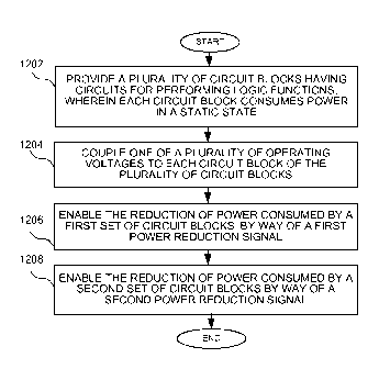
Turning now to Fig. 12, a flow chart shows a method of minimizing power
consumption in a device according to an embodiment of the present invention.
In particular, a plurality of circuit blocks having circuits for performing
logic
functions, such as programmable logic circuit blocks in devices having
programmable logic, are provided at a step 1202, wherein each circuit block
consumes power in a static state. One of a plurality of operating voltages is
coupled to each circuit block of the plurality of circuit blocks at a step
1204. The
reduction of power consumed by a first set of circuit blocks is enabled by way
of
a first power reduction signal at a step 1206. The reduction of power consumed
by a second set of circuit blocks is enabled by way of a second power
reduction
signal at a step 1208. The reduction in power consumed by the first and second
set of circuit blocks may be achieved by selectively disabling portions of the
circuits as described above with respect to Figs. 1-11.
Finally, turning to Fig. 13, a flow chart shows a method of minimizing power
consumption in a device according to an alternate embodiment the present
invention. In particular, a plurality of circuit blocks having circuits for
performing
logic functions is provided at a step 1302, wherein each circuit block
consumes
power in a static state. A plurality of power control signals is generated at
a step
1304, wherein each power control signal controls an operating voltage of the
plurality of operating voltages. A first operating voltage of a plurality of
operating
voltages is coupled to each circuit block of a first set of circuit blocks at
a step
1306. A second operating voltage of the plurality of operating voltages is
coupled to each circuit block of a second set of circuit blocks at a step
1306.
Finally, at least a portion of each circuit block of the second set of
function blocks
is disabled at a step 1310. The method of Fig. 13 may also employ any of the
circuits of Figs. 1-11 as described above, or using any other suitable
circuit.
It can therefore be appreciated that the new and novel circuit for and method
of
minimizing the power consumption in a device has been described. It will be
appreciated by those skilled in the art that numerous alternatives and
equivalents will be seen to exist which incorporate the disclosed invention.
As a
CA 02713142 2010-07-23
WO 2009/105485 PCT/US2009/034421
result, the invention is not to be limited by the foregoing embodiments, but
only
by the following claims.
16