Note: Descriptions are shown in the official language in which they were submitted.
CA 02713385 2015-10-27
1
Description
RF-TRANSCEIVER FRONT-END WITH IMPLICIT DIRECTION CONTROL FOR TIME
DIVISION MULTIPLE ACCESS COMMUNICATION USING SUBMICRON TECHNOLOGY
Embodiments of the presented invention pertain to the technical field of radio
frequency
(RF) transmitters and receivers shortly named transceivers, and in particular,
to RF-amplifiers in
antenna front-ends integrated on a single chip.
BACKGROUND
Most of the used blocks are already known technology like the symmetric
wideband
amplifier for the Power Amplifier represented by a differential amplifier in
cascode structure and
the common base (common gate) differential Low Noise Amplifier (LNA) in the
receiving path.
Also the use of transistors in Complementary Metal Oxide Semiconductor
Technology (CMOS)
for switches is well known. Especially n-type and p-type Metal Oxid
Semiconductor Field Effect
Transistors especially (NMOSFET and PMOSFET) are used to construct
Transmission Gates or
Analog Switches. Most of these basic circuits may be found in "Halbleiter-
Schaltungstechnik" of
Tietze and Schenk, published by Springer or "CMOS Analog Circuit Design" of
Allen and
Holberg published Oxford University Press.
The innovative step is represented in the implicit using of disabling the
transfer function
by manipulating the bias voltage at the gates and bulks of some transistors.
A typical RF-transceiver is presented in the Radio communication apparatus of
EP 1 176
709 A2 showing a typical front-end of actual designs. The need of a
disadvantageous additional
switch to commutate the transfer direction from and to the antenna is shown.
Most transceivers prefer common source configurations to common gate for the
LNA
especially resistively matched LNAs or feedback LNAs and inductively-
degenerated LNAs.
An Ultra Wide Band CMOS Transceiver with common gate input stage of NMOS
devices
has been presented by Razavi and others in IEEE Journal of Solid-State
Circuits Vol.40 in Dec
2005. This circuit also allows direct (implicitly) sharing of the receiver
antenna with the
transmitter.
A 0.18 pm Thin Oxide CMOS Transceiver Front-End with Integrated TX/RX
Commutator
for Low Cost Bluetooth Solutions has been published by Vincent Knopik and
Didier Belot of
STMicroelectronics in 2003 (ESSCIRC Poster 24). This Front-End does not use an
antenna
switch. The main idea is to put the device (either PA or LNA) in power down
mode when it is not
active. That solution uses only one pin for both RF-input and output. The LNA
impedance is
matched to the antenna, and the PA output's impedance is optimised for the
LNA. The LNA
uses common gate topology with NMOS devices.
CA 02713385 2015-10-27
2
TASK OF THE INVENTION
Based on existing technologies as quoted in the literature above, an
integrated circuit
was looked for, allowing low cost integration of radio-frequency (RF)
transceivers - especially for
quad-band ISM applications. To achieve cost reduction the number of antennas
and the number
of passive matching elements (Inductance, Capacitance and Resistance) should
be minimized.
Also the device area of silicon should be minimized.
Since the target application based on Time Division Duplex communication
allows the
usage of only one antenna, the need for transmit/receive (TX-RX switches)
should be avoided.
A primary task of the invention is to avoid the use of high frequency analog
signal switches
between the RE-port and the antenna. A further task is to use the same
matching elements for
both communication directions allowing a single configuration and adjustment
for broadcasting
and receiving. Finally, the RF-front-end amplifiers shall be designed to
achieve the required
signal quality and signal to noise ratio and the required signal damping of
the direction path
which isn't used. Beside NMOS devices the implementation of a PMOSFET in
common gate
configuration shall be considered in order to reduce the number of cost
intensive parts
compared to the given state of the art.
SUMMARY OF THE INVENTION
Only one antenna and the same matching elements for a wireless RF-transceiver
front-
end are required for both RE-communication directions with the help of
implicit direction controll.
Time division duplex communication is the basic requirement. This front-end is
primarly used in
Time Division Multiple Access Communication (TDMA) transceivers. A target
application is a
quad-band ISM transceiver. Used technologies are submicron-technologies
especially 0,18 pm
CMOS (Complementary Metal Oxide Semiconductors) or BiCMOS- (Bipolar CMOS)-
technology.
The front-end of the transceiver consists of two blocks that are processed on
the same
integrated circuit.
The first block shows a Power Amplifier (PA) output stage, which uses a
transistor
cascode circuitry in open-drain-configuration for the last stage of the signal
amplification to drive
an external connectable RF-antenna. Advantageous is that the cascode-
transistor is serving as
a common-gate-transistor with constant biasing during the broadcasting (TX)-
period. During
CA 02713385 2010-07-27
3
receive (RX) period controlling means are used to change the gate-potential of
the cascode
transistor in order to isolate the TX-path from the antenna.
The second block is a Low Noise Amplifier (LNA). Its input stage is
advantageously built
by a p-channel metal oxide semiconductor field effect transistor (PMOSFET) in
common-gate
configuration that implicitly is used to disconnect the RX-part of the
transceiver from the
antenna. In this case especially an enhancement type of PMOSFET is used. The
electrical
disconnection is supported through its bulk by means for changing the bulk's
voltage potential
from source voltage potential to a level above the source voltage potential.
In order to generate a receive-signal voltage-drop, the drain of the PMOSFET
of the LNA
input stage is electrically connected to a resistive load. A second amplifier
stage increases the
signal gain of the received signal to a suitable level especially for a radio
frequency signal
mixer. The gate of the PMOSFET is set to a low bias voltage during the RX
periods of the
transceiver. By forcing the gate to positive supply voltage the antenna
voltage is pinched off at
the input stage. This disables the receiving especially during broadcasting.
For test purposes it
may be possible to keep the RX path opened to read back the driving signal of
the PA. In this
case the gate may be controlled by changing the bias voltage during receiving
for damping the
output signal to a level required at the input of the LNA's deeper amplifier
stage. Beside the
modes for broadcasting, receiving and testing a fourth mode may be inactive,
which means the
antenna is high ohmic decoupled from the transceiver by it outmost active
elements.
As one aspect of the present invention and depending on the available
semiconductor
process, the main transistor of the cascode circuitry of the PA output stage
is a bipolar junction
npn-transistor or an n-channel metal oxide semiconductor field effect
transistor (NMOSFET). In
case of an NMOSFET an enhancement type is preferred. The base or respectively
the gate of
this output stage transistor is electrically connected to the output of a
preamplifier.
Another aspect of this invention is that the gate of the cascode transistor of
the PA is
applied to a higher voltage potential than the drain-voltage of this
transistor. This allows to get
rid of the voltage loss of the cascode-transistor due to its threshold voltage
at broadcasting.
Preferably a charge pump is used to generate the additional voltage potential
beyond
the positive supply voltage VDD and the negative supply voltage Vss which is
higher than VDD at
least the step of the threshold.
According to another aspect of this invention, an open drain terminal of the
PA output
stage and an open source terminal of the LNA input stage are electrically
connected and led to
the same port or connected at the same port of the integrated circuit. This
port is the antenna
connection port.
CA 02713385 2010-07-27
4
The matching elements are outside of the device and connected to a positive
supply
voltage VDD which drives the current either though the open drains of the PA
output stage or
through the open sources of the LNA input stage.
Especially if the open drain terminal of the PA output stage and the open
source terminal
of the LNA input stage are not connected to the same port, these terminals
advantageously
electrically contact the same antenna at least approximately at the same
point.
According to a further aspect of the invention, an open drain terminal of the
output stage
of the PA and an open source terminal of the input stage of the LNA use the
same additional
matching components. This allows reducing trimming or adjusting effort. The
main matching
component may be an external tuning coil, which is the same for both, the TX
part and the RX
part of the transceiver.
Another important aspect is that all stages of the amplifiers of the PA and
the LNA are
symmetrically differential amplifiers.
This results in a differential pair of outputs at the PA output stage and a
differential pair
of inputs at the LNA input stage. These differential input and output
terminals advantageously
use the same differential input-output terminal or are at least electrically
connected to the same
differentially driven antenna. The ports may be connected to suitable
connections of a loop
antenna. This antenna is unique and acting for both periods - for broadcasting
and receiving.
As a further aspect of the invention the differential outputs of the PA output
stage and
the differential inputs of the LNA input stage may be electrically connected
to the same
additional matching components especially to the same external tuning coil(s).
The innovation is detailed described in following preferred embodiments:
Fig.1 is a block diagram of a sample of an RF-transceiver circuit using the
invented front end.
Fig.2 is a detail 321 out of Fig.1 with the small difference that the
connection point 301 is
placed outside the front end I.
Fig.3 is a typical prior art configuration using high frequency TX/RX-
switches.
Fig.4 is a more detailed representation of the invented RE-transceiver front
end 1 according to
the detail 321 of block diagram in Fig.1, showing schemata of the preferred
embodiments of the
Power Amplifier (PA) 100 and the Low Noise Amplifier (LNA) 200 here only in a
non differential
incorporation.
Fig.5 shows the preferred differential solution of the RF-transceiver front
end 1.
CA 02713385 2010-07-27
=
Fig.6 is another embodiment comparable to Fig.4 using a bipolar junction
transistor instead of
the main NMOSFET in the PA.
Fig.7 shows the differential schematic according to Fig.6. Here, two matching
coils are involved
at the antenna.
A typical integrated RE-transceiver is modulating base band signals into upper
channels
for radio transmission and demodulating radio signals into base band. The
block diagram in
Fig.1 shows a crystal oscillator 400 as a reference frequency source and a
frequency generator
410. The frequency generator may be a voltage controlled oscillator in a phase
locked loop
architecture and allows defining the mixing frequency for the mixer 500 or it
allows to synthesize
and modulate the transmit-frequency. The (filtered) RE-output signal needs to
be amplified by
the PA 100. The output of the PA is normally connected to the broadcasting
antenna. The
matching elements are adapted to the requirements for best transmission.
In the RX-path a front end amplifier is required to bring the RF-signal of the
receiving
antenna to the input of a mixing stage 600 to get the RE-modulated data down
to the base
band. A digital to analogue signal converter (D/A) 700 and an analogue to
digital converter
(AID) 800 are shown in the example changing from the digital base band domain
into the analog
signal domain. Digital Signal Processing (DSP) 900 is carried out to bring the
data to and from
the required digital format. A Serial Interface (SI) 910 may be used to
communicate with other
integrated circuits like micro-controllers.
The application area is wide. All types of TDMA supported RE-communication
protocols
may use the structure, like Bluetooth-transceivers or Wireless Local Area
Network-interfaces
(WLAN). A quad band ISM transceiver is a favourite application of the
invention.
The invention is focused on part 321 in Fig.1. The rest of the integrated
circuitry is many-
faceted. The block 1 of the shown integrated circuit 2 is the transceiver
front-end. This is the
outmost part of the circuit towards the antenna 300. There is only one
(advantageously
differential) connection point 301 for the antenna to the integrated circuit
in this example. At this
point the RF-transmission-power is adaptively coupled into the antenna
resistance. The typical
supply voltage used in such a circuit is 1.8 Volt which is a process typical
value for 0.18 pm
CMOS or BiCMOS technologies. To supply the input stage of the receiver and the
output stage
of the transmitter, this point is connected to the supply voltage potential
VDD (here 1.8 Volt).
Matching elements 302 are foreseen to adjust the antenna and to filter the
required RE-
bandwidth. The input stage is a part of the LNA 200 and the output stage a
part of the PA 100.
Fig. 2 shows the RF-transceiver front-end that is considered in the presented
invention.
It is not necessary to combine the output of the PA and the input of the LNA
internally. In some
CA 02713385 2010-07-27
6
cases, especially for test purposes, it might be advantageous to lead both
connections to
separate ports and the short is carried out externally, compare the block
border 1 in Fig.1 to 1'
in Fig.2.
As most prior art circuits require special RF-suitable TX/RX switches that
need low noise
and low power loss and are not cheap in construction the presented invention
is a smart
alternative. To existing switchless transceiver-designs the advantage is
provided by the reduced
required components.
Fig.3 shows a typical prior art arrangement of a Time Division Duplex RF-front
end. In
many cases, the switches are situated outside the integrated circuit.
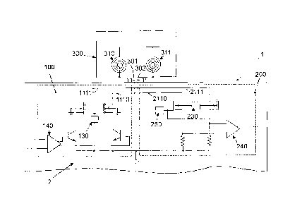
The main power amplifier output stage of the PA 100 is designed using a
cascode
circuitry in open drain configuration. In Fig.4 the main transistor 120 is an
NMOSFET
(enhancement type ¨normally off) whose gate is controlled by the output
voltage of a standard
Pre-Amplifier 140. Fig.6 shows an alternative bipolar junction transistor 120'
that may be
implemented in a BiCMOS process technology. The cascode transistor 110 in
these
configurations is an NMOSFET in common gate configuration while the PA is
active. Thus the
gate is switched to VDD during broadcasting active. The gate 112 of this FET
110 is controlled to
achieve the high ohmic disconnection from the antenna 300 and the matching
component. As
indicated in Fig.4 by block 130 this is done by forcing the gate to Vss or
ground potential. In a
0.18 pm process the typical voltage of 1.8V may be applied in transmission
mode. A switching
to a level above VDD minimizes the threshold voltage drop at the cascode
transistor. This voltage
need to be generated internally for example with the help of a charge pump.
Thus the bias at
the gate does not influence the transconductance of the main transistor 120 or
120' and the
resulting gain is depending on the resistive load connected to the open drain
antenna port.
A preferred embodiment of the PA is differential. The signal branches in Fig.4
and Fig.6
only show half of the realized design. The figures Fig.5 and Fig.7 show the
more detailed
schemata of the typical front-end configurations. Therefore the Pre-Amplifier
140 is differential
and has a differential input for the output of deeper structures (the HF-
synthesizer, modulator or
mixer). Each contact of the differential output of the Pre-Amplifier is
connected to one gate or
one base of the main transistors (NMOSFET (Fig.5) or BJT (Fig.7)). These form
together with
the cascode- NMOSFETs a differential amplifier in cascode-circuit.
The controlling signal for the gates of the cascode NMOSFETs can be the same.
The
source represents the enable/disable signal for the broadcasting and is
controlled from digital
parts of the transceiver. The gates of the differential amplifier are switched
off by setting the
level to ground Vss. In broadcasting the gates are forced to signal VDD or to
a higher internal
CA 02713385 2015-10-27
7
generated voltage VDD++. The open drain outputs of the differential amplifier
are connected to
the matching elements and the antenna. This antenna is a loop antenna 300 in
the examples of
Fig.5 and Fig.7. In Fig.7 a coil represents the major matching element for
each single ended
output. These represents a certain inductance that is connected to VDD. This
VDD is the supply
voltage of the output stage. Instead of two coils also one coil can be
connected as a matching
element. This is demonstrated in Fig.5.
Taking a closer consideration to the LNA 200 in Fig.2, the single ended
embodiment of
the LNA is shown in Fig.4 (and Fig.6). A common gate structure with resistive
load 220 at the
drain 213 incorporates the LNA primary stage. The output of a PMOSFET 210
(enhancement
type ¨normally off) ¨ amplifier is connected to a second amplifier stage 240.
The behaviour of
the PMOSFET 210 changes from active to disabled by changing the bias voltages
at the bulk
214 and the gate 212 of the transistor 210 with the controlling blocks 230 and
250. The bulk
controlling block 230 provides a positive supply voltage potential VDD in
receiving mode and a
separate reference voltage VDD++ which is higher than VDD during broadcasting
mode. The
additional voltage may be internally generated, and could be the same
potential as described
above for the gate 112 of the cascade transistor 110 during broadcasting. The
forced high bulk
voltage prevents infringing the broadcasting by the source of the PMOSFET 210.
The gate controlling block 250 provides the bias voltage for the operating
point of the
common gate configuration in receiving mode and is forced to ground to turn
off the PMOSFETs
source-drain connection.
The LNA 200 also should be designed symmetric differential as shown in Fig.5
and
Fig.7. In this case the 2nd stage amplifier is differential too and contacts
the differential output of
the PMOSFETs. The blocks 230 and 250 for providing the bulk and the gate
biasing (or to
disable the input stage) of the Low Noise Differential Amplifier can be
connected to both bulks -
respectively gates of the transistor pair.
This concept allows to share the TX-output or differential TX output port of
the PA with
the RX-input or differential RX input port of the LNA without any analog
switch. The drain 111 of
the NMOSFET 110 can be connected to the source 211 of the PMOSFET 210 having
only low
impact on the matching configuration (Fig.4, Fig.6). In differential
configuration the drains
1110,1111 are directly connected to the sources 2110,2111.
*****