Note: Descriptions are shown in the official language in which they were submitted.
CA 02713638 2010-07-29
WO 2009/108831 PCT/US2009/035401
-1-
A TUNABLE OPTICAL DISCRIMINATOR
Field of the Invention
The present invention relates to the control of optical discriminators. It
finds
particular utility in the control of discriminators in long haul optical
communications
systems.
Background to the Invention
In optical communications systems data is imparted onto light by varying the
intensity
and/or phase of the light signal. In a simple example binary data may be
signaled by
emitting light of maximum intensity to represent a "1" and zero intensity to
represent
a "0". An optical format of this kind, where the data is represented by the
amplitude
of the signal, is known as amplitude shift keyed (ASK).
In addition to ASK formats, it is known to transmit over long haul optical
communications using phase-shift keyed (PSK) formats. Examples of PSK formats
include differential PSK (DPSK) and differential quadrature PSK (DQPSK). PSK
formats impart information onto the optical signal by varying its phase
(rather than its
intensity).
Data transmitted optically is typically manipulated in electronic form at its
destination.
Optical receivers for use in optical communications systems are therefore
capable of
converting optical signals into electronic signals. This is a relatively
simple process
for ASK formats, where components such as photo-diodes) for example, positive
intrinsic negative (PIN) diodes) can be used to generate a signal which is
proportional to the intensity of the received light. However, such components
are
typically incapable of discriminating between the phase of incident signals,
and so
additional features are required to decode PSK formats.
In particular, optical discriminators (differential delay interferometers) are
used to
extract the information included in PSK signals. Discriminators of this type
typically
split an incoming PSK signal into two components, and apply a relative delay
to one
of these components before they are recombined. By setting the delay as an
integer
number of the time period for a data bit in the signal, an initial bit can be
compared
with a subsequent bit through the interference of the two when the components
are
combined. The overall amplitude of the signal will consequently represent the
difference in phase between these two bits. Since the amplitude can be
measured
CA 02713638 2010-07-29
WO 2009/108831 PCT/US2009/035401
-2-
by conventional components, the difference between the two bits can then be
inferred from the resultant signal.
Reception of DPSK data requires accurate relative wavelength tuning control
between the transmit signal carrier wavelength and the receiver optical
discriminator
such that the two remain accurately locked to each other. It is not possible
to fix the
tuning point(s) since the practical inherent stability of the transmitter
laser source and
the receiver discriminator cannot be relied upon to maintain good performance.
It is known, and conventionally preferred, to keep the transmit laser
wavelength
nominally fixed and to lock the receiver discriminator by a feedback control
loop that
measures receiver performance. An example of such a device is shown in US
patent
application US 2006-133827, which is incorporated herein by reference. The
device
in this application uses a dither based control loop which adjust the
temperature
experienced by one of the separated components passing through the
discriminator,
thereby altering the relative delay experienced by the two components before
they
are combined. The electrically detected radio frequency (RF) peak voltage as
measured at a receiver photodiode is measured for higher and lower
temperatures,
and the temperature of the discriminator is adjusted towards the temperature
in
which a higher peak voltage is measured. Eventually, the device reaches an
equilibrium position where alteration of the temperature would be
disadvantageous in
either direction, and the discriminator may be considered tuned to the carrier
frequency of the optical signal.
Although thermal control of the discriminator wavelength described above may
lead
to improved results, it has an inherent and usually long time constant.
Furthermore,
as the direction in which to tune the discriminator is also established by
variation of
the discriminator control temperature, the thermal time constant of the
discriminator
also limits the speed at which this can be done. The combination of a thermal
time
constant and the requirement of dithering, means control is cumbersome and
slow.
Moreover, further difficulties occur in practice as discriminators usually
incorporate a
heater rather than a thermo-electric cooler (TEC), for component fabrication
simplicity, and as a result the dithering process relies on temperature decay
to set
the upper dither rate (that is, the process is even slower than would be the
case for a
device that could be actively cooled).
It is also found that to achieve a dither amplitude that offers a satisfactory
results, a
significant varying heat flux is required. This can lead to premature
component
failure. This is compounded by the fact the heater has to run at an elevated
CA 02713638 2010-07-29
WO 2009/108831 PCT/US2009/035401
-3-
temperature with respect to the ambient in order to produce a tuning reaction -
the
higher the temperature with respect to ambient the faster the temperature
decay for
dither, but also the more component stress. As well as limiting the
effectiveness of
these techniques in adjusting the discriminator during use, the slow control
loop can
also hinder start-up time from cold before satisfactory transmission can be
achieved.
Summary of the Invention
According to the first aspect of the present invention, there is provided an
optical
transmission system comprising:
an optical source for transmitting an optical signal at a carrier frequency;
an optical discriminator for receiving the optical signal, the optical
discriminator having an output; and,
a controller adapted to dither the carrier frequency to obtain a relationship
between a signal quality metric at the output and the carrier frequency, the
controller
being further adapted to tune the optical discriminator or the carrier
frequency in
dependence on the relationship.
The present invention uses variation of the optical carrier frequency to tune
one or
more components in an optical system. In particular, the performance of the
discriminator may be improved without the need to test it at number of tuning
points.
In this way, the time-consuming alteration of the tuning position of the
discriminator is
limited to positive improvements in performance (if required at all) rather
than being
used for test purposes. Variation of the carrier frequency is faster and more
efficient
for this purpose than prior art techniques. Once the testing stage has been
carried
out by the dithering technique the components are then tuned so as to improve
the
quality metric.
In a preferred embodiment, the optical signal is differential phase shift
keyed (DPSK).
In another preferred embodiment, the optical signal is differential quadrature
phase
shift keyed (DQPSK). However, other data formats may used for optical signal.
The carrier signal and the discriminator may be tuned in a number of ways. In
particular, preferred embodiments tune the discriminator by varying its
operating
temperature, and tune the carrier frequency by varying the operating
temperature of
the signal source.
Preferably, the carrier frequency is dithered by varying a current driving the
optical
source. The variation of the drive current of the optical source is relatively
fast when
compared with other techniques, such as temperature control. This allows the
CA 02713638 2010-07-29
WO 2009/108831 PCT/US2009/035401
-4-
system to be tuned at a greater speed since the relationship between carrier
frequency and output quality can be identified at much greater speed. As such,
preferred embodiments first perform the dithering process for the carrier
frequency
by varying the current driving the source, before subsequently tuning the
source by
control of the temperature of the source. This ensures a relatively quick
response
during the dithering process while enabling stable control of the tuning of
the source
through temperature control.
The output quality may be bit error rate (BER) or any other known metric used
to
describe the quality of received data (for example Q value or peak RF
voltage).
Moreover, the output quality may be a combination of metrics according to any
desired relationship.
The dithering and tuning of the components may occur on a one-off basis, for
example during the set-up of the system. However, the controller is preferably
adapted to dither the carrier frequency and tune the optical discriminator or
the
carrier frequency during operation of the optical transmission system. More
preferably, the controller is adapted to continuously dither the carrier
frequency and
tune the optical discriminator or the carrier frequency during operation of
the optical
transmission system.
The optical signal source is preferably a laser. The laser is preferably a
continuous
wave laser.
The controller may be located either at the receiver or transmitter end of the
optical
system, or may be distributed between the two.
According to a second aspect of the present invention, there is provided a
method for
tuning components in an optical system, the method comprising:
transmitting an optical signal to an optical discriminator having an output,
the
optical signal having a carrier frequency;
dithering the carrier frequency to obtain a relationship between a signal
quality metric at the output and the carrier frequency
tuning the carrier frequency or the discriminator in dependence on the
relationship.
According to a third aspect of the present invention, there is provided an
optical
transmitter, comprising:
an optical source for transmitting an optical signal at a carrier frequency to
an
optical discriminator having an output, and
a controller adapted to dither the carrier frequency to obtain a relationship
CA 02713638 2010-07-29
WO 2009/108831 PCT/US2009/035401
-5-
between a signal quality metric at the output and the carrier frequency, the
controller
being further adapted to tune the optical discriminator or the carrier
frequency in
dependence on the relationship.
According to a fourth aspect of the present invention, there is provided an
optical
receiver, comprising:
a discriminator having an output for receiving an optical signal having a
carrier
frequency, and
a controller adapted to dither the carrier frequency to obtain a relationship
between a signal quality metric at the output and the carrier frequency, the
controller
being further adapted to tune the optical discriminator or the carrier
frequency in
dependence on the relationship.
Brief description of the drawings
Examples of the present invention will now be described in detail with
reference to
the accompanying drawings, in which:
Figure 1 illustrates the position of a discriminator in a transmission system
that may
be used in accordance with the present invention;
Figure 2A is a schematic diagram of a discriminator based on a Mach Zehnder
interferometer;
Figure 2B is a schematic diagram of a discriminator based on a Michelson
interferometer;
Figure 3 illustrates the response curve of a discriminator relative to a
wavelength
offset;
Figure 4 illustrates the performance of a discriminator relative to a
wavelength offset;
and,
Figure 5 is a schematic diagram illustrating a feedback mechanism that may be
adopted in accordance with the present invention.
Detailed Description
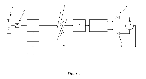
Figure 1 shows the architecture of a typical transmission system incorporating
a
discriminator, such as may be adopted in the context of the present invention.
The
example shown in Figure 1 is used for the transmission of differential phase
shift
keyed (DPSK) data, although other data formats may be used in the context of
the
present invention. In particular, other phase shift keyed formats (such as
differential
quadrature phase shift keyed (DQPSK)) may be adopted in accordance with the
CA 02713638 2010-07-29
WO 2009/108831 PCT/US2009/035401
-6-
present invention.
A continuous wave laser source 10 emits a light signal having a carrier
frequency.
The laser source 10 is coupled to a thermoelectric cooler (TEC) 12 in order to
regulate its temperature. Data is then modulated onto the source signal at a
data
frequency by a phase modulator 14 driven by a differential encoder 16. As
mentioned above, the resulting data format is DPSK. The data modulated optical
signal that results is simply binary modulated with data bits represented by 0
or 180
degrees phase. Preferably, an additional sinusoidal modulation (not shown in
the
Figure) is applied at the data frequency in order to produce a return to zero
(RZ)
signal. The resulting RZ-DPSK format has been found to be extremely favourable
in
long-haul transmission applications.
The data modulated signal then passes across a transmission system 20. This
transmission network 20 may in practice be extremely large (for example in
long-haul
submarine optical communications tasks) and may contain a number of repeaters
along the transmission path.
Although not shown, and not essential to the present invention, the modulated
optical
signal transferred across the transmission system is typically one of many in
a
wavelength division multiplexed (WDM) signal. A WDM signal contains a
plurality of
individual modulated signals each having a distinct carrier frequency. In this
way, a
plurality of data communications may be transmitted down a single transmission
line
simultaneously.
After passing through the transmission system 20 the signal is selected from
those
carried by the WDM signal by a channel filter 30. The filtered signal is then
passed
to a discriminator 32.
The discriminator 32 is typically a differential delay interferometer. In such
devices,
the signal is divided into two components, one of which is delayed relative to
the
other, and then recombined. A first output port 34 receives light in the case
that the
two components interfere constructively (that is, in the case where the two
components are in phase), while a second output port 36 receives light when
the two
components interfere destructively (that is, in the case where the two
components
have opposite phase).
The output ports allow the representation of the data bits (which, as
mentioned
above are encoded in the phase of the signal transmitted over the transmission
system) to be detected as amplitude modulation at photo diodes. This process
is
one of differential decoding which allows the data imparted by the
differential
CA 02713638 2010-07-29
WO 2009/108831 PCT/US2009/035401
-7-
encoder to be retrieved. Advantageously, the signals provided by the
photodiodes
may be subtracted from each other by a logic device (such as a differential
amplifier)
38 to provide a BER performance benefit in terms of optical signal to noise
ratio
(OSNR) tolerance as compared with typical techniques employing amplitude shift
keying (ASK).
Figures 2A and 2B illustrate broadly the architecture of possible
interferometers that
may be used in the context of the present invention. Figure 2A illustrates an
interferometer of the Mach Zehnder (MZ) type, while Figure 2B illustrates a
Michelson interferometer. Each interferometer has a constructive port 201
through
which light propagates when the separate components are recombined in phase,
and
a destructive port 202 through which light propagates when light is combined
out of
phase.
In the case of a MZ interferometer the incoming signal 205 is divided into two
components by a 50/50 coupler 210 and the light in one of these components is
subsequently delayed with respect to the other by a path length 212, before
they are
recombined by a combiner 214. The delay may be applied by increasing the
physical distance through which the delayed component must travel with respect
to
the other component, but may also be slightly altered by increasing the
refractive
index of the waveguide through which the delayed component passes, thereby
increasing the optical path length.
The Michelson delay interferometer shown in Figure 2B divides the incoming
signal
205 into two components through use of a half silvered mirror 220. The two
components are then reflected by mirrors 222 before recombining at the half
silvered
mirror 220. Again, the path length of each component is different in order to
ensure
that one component is delayed with respect to the other.
In order to implement differential decoding of the transmitted signal, the
delay
between the two components in the interferometer is an integer multiple of the
bit
period. Preferably, the delay is chosen as one data bit period. For example,
in a
10Gb/s system, the delay would be 100ps, which equates physically to about 2cm
in
glass. This delay will set the free-spectral range, or repeat period, of the
device in a
spectral sense. Figure 3 shows a typically example (in this case the
demodulator is
suitable for receiving a 10.709Gb/s DPSK signal), illustrating the measured
spectral
response at the constructive 301 and destructive 302 ports as a function of
wavelength. This would be measured with either tunable CW laser or a broadband
noise source.
CA 02713638 2010-07-29
WO 2009/108831 PCT/US2009/035401
-8-
Optimal reception of the optical signal will occur when the discriminator's
spectral
response is correctly aligned to the transmitter signal. Typically the
discriminator will
be tunable by some mechanism in order to achieve this alignment. For example,
the
relative delay experienced by each component in the discriminator may be
altered.
In some preferred embodiments, the relative path length delay may be adjusted
by
an amount in the order of one carrier wavelength of the transmitted light. The
adjustment of the delay may be achieved by physically altering the nature of
the
optical path traveled by one of the components. For example, the differential
delay
may be adjusted by temperature control of a glass waveguide in order to cause
bulk
expansion or contraction.
Alignment of the discriminator response with the transmitter wavelength may
alternatively be achieved tuning the transmitter wavelength itself. Moreover,
a
combination of adjustment of the discriminator and the transmitter may be used
to
achieve the requisite tuning.
In practice, the tuning between the transmitter wavelength and discriminator
response must be constantly updated to take account of changing conditions. A
system that is set up at the optimum tuning initially will not retain suitable
alignment
over the lifetime of the system. Typical reasons for this include laser aging
that
requires more injection current to maintain a given output power, the
increased
current having the effect of increasing the refractive index in the laser's
active region,
which in turn leads to a lower lasing frequency. Thermal and environmental
conditions can also affect both the laser and discriminator alignment. This
will occur
despite the fact that the laser is typically thermally stabilized using a TEC
and
thermistor feedback temperature measurement as it is physically difficult to
measure
the actual laser temperature accurately, leading to an error related to the
distance
between the thermistor chip and the laser itself. Thermal flux can also de-
tune the
discriminator if it is not coupled to the optical paths (or waveguides) of
both
components equally.
Figure 4 demonstrates the sensitivity of receiver performance to the tuning of
the
discriminator to the transmitter wavelength. In practice, it is found that,
for a 10Gb/s
system, a 0.25 GHz delta drift between the transmit laser and the receiver
discriminator may be accommodated without an unacceptable performance penalty
in terms of bit error rate (BER).
In order to continuously align the discriminator and the transmitter (carrier)
wavelength, the carrier wavelength is rapidly dithered in order to obtain
performance
CA 02713638 2010-07-29
WO 2009/108831 PCT/US2009/035401
-9-
information showing the relationship of a signal quality metric at the output
of the
discriminator (such as BER) and the carrier wavelength. That is, various
carrier
wavelengths are adopted in relatively quick succession and performance
measures
are taken at each of these wavelengths. The carrier wavelength and/or the
discriminator settings can then be adjusted towards the value at which the
best
performance measure is achieved. The information obtained in this way allows
the
characteristics of the transmitter and the discriminator to be tuned
effectively, without
time consuming trial and error. In particular, there is no requirement to
adjust the
discriminator repeatedly and take measurements at each setting in order to
ascertain
to correct tuning of the discriminator.
Figure 5 shows an optical system that may be used in accordance with the
present
invention. The features depicted in Figure 5 that are equivalent to those
shown in
Figure 1 have the same reference numerals and perform the same functions.
A continuous wave (CW) signal laser 10 is powered by a current source 66 and
normally also temperature stabilised in order to define its operating
wavelength using
a TEC 12. It is possible to adjust the lasing wavelength by changing the laser
temperature (increasing the temperature gives a longer wavelength). However,
the
wavelength may be more quickly altered by changing the injection current
(drive
current) used to drive the laser. Increasing the injection current of the
laser
semiconductor medium and lengthens the lasing wavelength, while decreasing the
drive current does the opposite. For a typical 1550nm telecom laser this
tuning is of
order -1 GHz/mA, and the total drive current of order 100mA. As such, an
insignificant
change in laser output power will be seen if it is dithered with 0.5mA peak to
peak.
As noted in Figure 4, a variation of +/-0.25GHz would be appropriate for
10Gb/s
transmission, since it would not add a substantial performance penalty.
As illustrated, the control scheme for optimizing the alignment of the
discriminator
and the carrier wavelength is distributed between the transmitter and the
receiver. As
such, the transmitter works in co-operation with the non co-located receiver.
In the preferred embodiment shown in Figure 5, the signals transmitted across
the
network 20 include forward error correction (FEC) imparted to the signal by a
FEC
encoder 18 coupled to the differential encoder 16. The signal then passes
across
the network to the discriminator 32. The outputs of the photodiodes at the
constructive 34 and destructive ports 36 of the discriminator are subtracted
and
subsequently decoded by a forward error correction (FEC) decoder 42. This step
produces measurements of bit error rate (BER) which are passed to a receiver
CA 02713638 2010-07-29
WO 2009/108831 PCT/US2009/035401
-10-
microprocessor 40. The microprocessor 40 works in combination with a return
transmitter 52 coupled to its own FEC encoder 50 for transmitting instruction
messages across a return transmission line 70 to a secondary receiver 54
coupled to
a further FEC decoder 56 where the instruction messages are retrieved. These
instruction messages are passed to a transmitter microprocessor 60. The
transmission microprocessor 60 then controls the drive current of the laser 10
and
the current driving the TEC 12 coupled to the laser via a number of digital-to-
analog
converters (DACs) 64.
In the preferred embodiment described above, the control intelligence resides
in the
receive location (in the receiver microprocessor 40) and transmits command
signals
to the transmitter contained in the return transmission line's FEC overhead
channel.
Equally, the control intelligence may reside in the transmitter and receive
the
performance data from the receiver. However, this approach requires
transmission
of instructions for the discriminator to be tuned to be transmitted across the
network.
The control scheme is preferably predominantly implemented as a software
algorithm
due to the practical convenience and flexibility of this approach.
The transmitter contains circuitry that both adjusts laser injection current
and also
stabilises its operating temperature with current source connected through the
laser's
TEC. Typically these currents are defined by a micro-processor driving DACs 64
which in turn are connected to power semiconductors 66.
Commands from the far end receiver are communicated over the return
transmission
line, received by the FEC decoder 56 and executed to drive either the laser
injection
current or the laser temperature. The receiver microprocessor 40 implements a
transmit laser dither cycle by sending appropriate commands at the correct
times. In
turn, the transmission performance is measured by methods of error detection
from
the FEC (alternatively or additionally, a RF peak detector rectifying the
electrical
signal from the receiver PIN may be used as a measure of transmission
quality).
Performance improvements would be deemed a reduced transmission BER (or
increased RF peak voltage) in the case of RZ-DPSK (or RZ-DQPSK).
Optimisation of performance with respect to laser-discriminator wavelength
offset
may be achieved by tuning the discriminator heater control. This heat control
is
driven by a current source 46 controlled by the receiver microprocessor 40 via
a DAC
44. Alternatively, and in some cases beneficially, performance can also be
optimised by tuning the discrete laser temperature and leaving the
discriminator fixed
(this has certain benefits that will be discussed later).
CA 02713638 2010-07-29
WO 2009/108831 PCT/US2009/035401
-11-
A first control algorithm that may be used, in the case in which the
discriminator is
tuned, may take the following form:
Start Loop:
Increase TX laser current by 0. 5mA
Measure RX BERI
Decrease TX laser current by 0. 5mA
Measure RX BER2
If(BER2>BERI) Increase RX Discriminator Wavelength
If(BERI>BER2) Decrease RX Discriminator Wavelength
Repeat Loop:
An alternative algorithm, in the case where the discriminator is fixed and the
laser
wavelength is tuned, may take the following form:
Start Loop:
Increase TX laser current by 0. 5mA
Measure RX BERI
Decrease TX laser current by 0. 5mA
Measure RX BER2
lf(BER2>BERI) Increase TX Laser Wavelength (i.e. increase temperature)
lf(BERI>BER2) Decrease TX Laser Wavelength (i.e. decrease temperature)
Repeat Loop:
In both of the above algorithms, the dithering of the transmitter wavelength
for testing
purposes is achieved by varying the drive current of the laser, while the
subsequent
tuning of the component (either laser or discriminator) is effected by
temperature
control. As such, the power of the laser once the system has been tuned is
unaltered as compared with the initial state.
One skilled in the art will recognise that by tuning the laser while leaving
the
discriminator fixed (as in the second algorithm above), the carrier laser
wavelength is
effectively locked to the receiver discriminator using it as a wavelength
reference,
providing stability for the carrier wavelength.
In a WDM system where a plurality of separate laser signals (or channels) are
transmitted at different frequencies across the network, each channel having a
different carrier frequency, the use of one or more fixed discriminators may
be used
to set and maintain the frequency spacing of the channels. For example, a the
free
spectral range of the device when receiving 10GB/s data coded with
conventionally
available FEC is 10.709GHz. As such, the use of a single discriminator for all
CA 02713638 2010-07-29
WO 2009/108831 PCT/US2009/035401
-12-
channels, or similarly specified discriminators for each channel, can be used
to lock
each channel of the system at a separation of 10.709GHz (since the
discriminator
has a repeating characteristic). For example a set of 4 channels across
42.836Ghz
may be used. If it is desired to distribute the channels across alternative
ranges (for
instance, it is known to distribute channels across a fixed grid such as
50GHz) then
the discriminator for each channel may be specifically tuned to normalise its
performance for a particular slot across the range.
It is found that the potential wavelength drift of the discriminator which is
identified
and addressed in the tuning algorithms above is not of such magnitude as to
interfere with reliable channel spacing when using the discriminator to lock
the
wavelengths of the lasers. Discriminators having suitable characteristics for
this
purpose are available commercially, for example from Optoplex Corp, in either
passive or semi-tunable form. A tunable discriminator that may be used with
the
present invention is described at
http://www.optoplex.com/pdf/DPSK-demodulator.pdf.
Fixed discriminator settings in 10Gb/s may also be used in the context of
three
channel systems across 3x10.709=32.127GHz, and two channel systems across
2x10.709=21.418GHz. This latter approach may find particular utility in the
systems
adopting DQPSK, given the additional spectral efficiency of this format.
In addition to offering benefits in terms of the control of channel spacing,
fixed
discriminator settings allow simpler construction leading to reduced cost.
In embodiments using a tunable discriminator, it may be found that the
discriminator
is only tunable across a set range. For example, the temperature of the
discriminator
may be limited to within certain limits. As such, it is desirable that the
algorithm
controlling the tuning of the discriminator to the wavelength of the laser
does not
force the discriminator beyond these limits.
Preferred embodiments of the present invention address the above-mentioned
problem by adjusting the wavelength of the laser in addition to the tuning of
the
discriminator in order to ensure that the discriminator remains within
acceptable
limits. For example, in addition to a step of tuning the discriminator a step
of
adjusting the wavelength is incorporated, wherein the step of adjusting the
wavelength depends on the relative position of the tuning of the discriminator
within
the available range. An exemplary algorithm of this type is given below:
Start Loop:
Increase TX laser current by 0.5mA
CA 02713638 2010-07-29
WO 2009/108831 PCT/US2009/035401
-13-
Measure RX BERI
Decrease TX laser current by 0. 5mA
Measure RX BER2
If(BER2>BERI) Increase RX Discriminator Wavelength
If(BERI>BER2) Decrease RX Discriminator Wavelength
If(Discriminator Wavelength>MID wavelength)
Decrease Laser Wavelength (i.e. decrease temperature)
If(Discriminator Wavelength<MID wavelength)
Increase Laser Wavelength (i.e. increase temperature)
Repeat Loop:
As can be seen the discriminator is first tuned to the laser wavelength in
dependence
on results obtained by dithering the laser wavelength, and the laser
wavelength is
then adjusted to bring it towards the centre of the range over which the
discriminator
may be tuned. In this example, the initial dithering of the laser wavelength
is
achieved by varying the drive current, while the later adjustment of the laser
wavelength is achieved by altering the laser temperature. This is appropriate
because varying the drive current has a direct effect on optical output power
of the
laser, but is achievable at the relative fast rate required to dither the
laser without
delay, while the slower time constant of varying the laser temperature is not
disadvantageous for the permanent adjustment used to bring the wavelength
towards the centre of the acceptable range for the discriminator.
The result of the technique outlined above is that the laser wavelength
remains
locked to the discriminator as required for good reception and the
discriminator is
held at its mid wavelength range for good control authority. This leads to a
robust
and reliable control solution with benefits that channel spacing is adequately
maintained by broad discriminator stability and fast control authority is
governed by
the laser dither control loop. In addition arbitrary channel spacing may be
achieved
with no pre-fixation of the discriminator component specification.